Precision, Very Low Noise, Low Input Bias Current, Wide Bandwidth JFET Operational Amplifier AD8610/AD8620
FEATURES
Low noise: 6 nV/√Hz Low offset voltage: 100 μV maximum Low input bias current: 10 pA maximum Fast settling: 600 ns to 0.01% Low distortion Unity gain stable No phase reversal Dual-supply operation: ±5 V to ±13 V
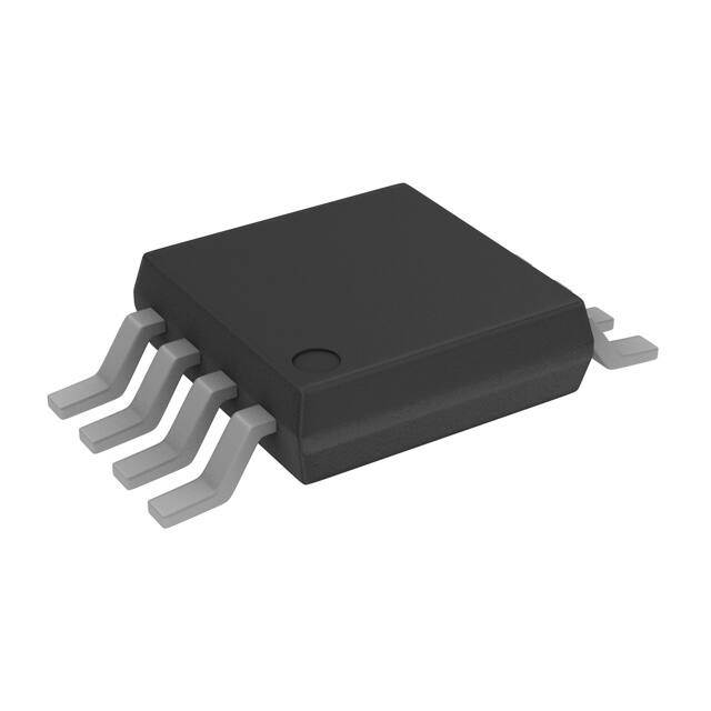
PIN CONFIGURATIONS
NULL 1 –IN 2 +IN 3
8
NC V+
AD8610
7
NC = NO CONNECT
Figure 1. AD8610 8-Lead MSOP and SOIC_N
OUTA 1 –INA 2 +INA 3
8
V+ OUTB
APPLICATIONS
Photodiode amplifier ATE Instrumentation Sensors and controls High performance filters Fast precision integrators High performance audio
AD8620
7
Figure 2.AD8620 8-Lead SOIC
GENERAL DESCRIPTION
The AD8610/AD8620 are very high precision JFET input amplifiers featuring ultralow offset voltage and drift, very low input voltage and current noise, very low input bias current, and wide bandwidth. Unlike many JFET amplifiers, the AD8610/AD8620 input bias current is low over the entire operating temperature range. The AD8610/AD8620 are stable with capacitive loads of over 1000 pF in noninverting unity gain; much larger capacitive loads can be driven easily at higher noise gains. The AD8610/ AD8620 swing to within 1.2 V of the supplies even with a 1 kΩ load, maximizing dynamic range even with limited supply voltages. Outputs slew at 50 V/μs in either inverting or noninverting gain configurations, and settle to 0.01% accuracy in less than 600 ns. Combined with high input impedance, great precision and very high output drive, the AD8610/AD8620 are ideal amplifiers for driving high performance ADC inputs and buffering DAC converter outputs. Applications for the AD8610/AD8620 include electronic instruments; ATE amplification, buffering, and integrator circuits; CAT/MRI/ultrasound medical instrumentation; instrumentation quality photodiode amplification; fast precision filters (including PLL filters); and high quality audio. The AD8610/AD8620 are fully specified over the extended industrial (−40°C to +125°C) temperature range. The AD8610 is available in the narrow 8-lead SOIC and the tiny 8-lead MSOP surface-mount packages. The AD8620 is available in the narrow 8-lead SOIC package. 8-lead MSOP packaged devices are available only in tape and reel.
Rev. E
Information furnished by Analog Devices is believed to be accurate and reliable. However, no responsibility is assumed by Analog Devices for its use, nor for any infringements of patents or other rights of third parties that may result from its use. Specifications subject to change without notice. No license is granted by implication or otherwise under any patent or patent rights of Analog Devices. Trademarks and registered trademarks are the property of their respective owners.
One Technology Way, P.O. Box 9106, Norwood, MA 02062-9106, U.S.A. Tel: 781.329.4700 www.analog.com Fax: 781.461.3113 ©2006 Analog Devices, Inc. All rights reserved.
02730-002
6 –INB TOP VIEW V– 4 (Not to Scale) 5 +INB
02730-001
6 OUT TOP VIEW V– 4 (Not to Scale) 5 NULL
�AD8610/AD8620 TABLE OF CONTENTS
Features .............................................................................................. 1 Applications....................................................................................... 1 Pin Configurations ........................................................................... 1 General Description ......................................................................... 1 Revision History ............................................................................... 2 Specifications..................................................................................... 3 Electrical Specifications............................................................... 4 Absolute Maximum Ratings ............................................................5 Typical Performance Characteristics ..............................................6 Theory of Operation ...................................................................... 13 Functional Description.............................................................. 13 Outline Dimensions ....................................................................... 22 Ordering Guide .......................................................................... 22
REVISION HISTORY
11/06—Rev. D to Rev. E Updated Format..................................................................Universal Changes to Table 1............................................................................ 3 Changes to Table 2............................................................................ 4 Changes to Outline Dimensions................................................... 21 Changes to Ordering Guide .......................................................... 21 2/04—Rev. C to Rev. D. Changes to Specifications ................................................................ 2 Changes to Ordering Guide ............................................................ 4 Updated Outline Dimensions ....................................................... 17 10/02—Rev. B to Rev. C. Updated Ordering Guide................................................................. 4 Edits to Figure 15............................................................................ 12 Updated Outline Dimensions ....................................................... 16
5/02—Rev. A to Rev. B Addition of part number AD8620 ...................................Universal Addition of 8-Lead SOIC (R-8 Suffix) Drawing............................1 Changes to General Description .....................................................1 Additions to Specifications ..............................................................2 Change to Electrical Specifications.................................................3 Additions to Ordering Guide...........................................................4 Replace TPC 29..................................................................................8 Add Channel Separation Test Circuit Figure.................................9 Add Channel Separation Graph ......................................................9 Changes to Figure 26...................................................................... 15 Addition of High-Speed, Low Noise Differential Driver section .............................................................................................. 16 Addition of Figure 30..................................................................... 16
Rev. E | Page 2 of 24
�AD8610/AD8620
SPECIFICATIONS
@ VS = ±5.0 V, VCM = 0 V, TA = 25°C, unless other wise noted. Table 1.
Parameter INPUT CHARACTERISTICS Offset Voltage (AD8610B) Offset Voltage (AD8620B) Offset Voltage (AD8610A/AD8620A) Symbol VOS –40°C < TA < +125°C VOS –40°C < TA < +125°C VOS +25°C < TA < +125°C –40°C < TA < +125°C Input Bias Current IB –40°C < TA < +85°C –40°C < TA < +125°C Input Offset Current IOS –40°C < TA < +85°C –40°C < TA < +125°C Input Voltage Range Common-Mode Rejection Ratio Large Signal Voltage Gain Offset Voltage Drift (AD8610B) Offset Voltage Drift (AD8620B) Offset Voltage Drift (AD8610A/AD8620A) OUTPUT CHARACTERISTICS Output Voltage High Output Voltage Low Output Current POWER SUPPLY Power Supply Rejection Ratio Supply Current/Amplifier DYNAMIC PERFORMANCE Slew Rate Gain Bandwidth Product Settling Time NOISE PERFORMANCE Voltage Noise Voltage Noise Density Current Noise Density Input Capacitance Differential Mode Common Mode Channel Separation f = 10 kHz f = 300 kHz CMRR AVO ΔVOS/ΔT ΔVOS/ΔT ΔVOS/ΔT VOH VOL IOUT PSRR ISY VCM = –1.5 V to +2.5 V RL = 1 kΩ, VO = –3 V to +3 V –40°C < TA < +125°C –40°C < TA < +125°C –40°C < TA < +125°C RL = 1 kΩ, –40°C < TA < +125°C RL = 1 kΩ, –40°C < TA < +125°C VOUT > ±2 V VS = ±5 V to ±13 V VO = 0 V –40°C < TA < +125°C RL = 2 kΩ AV = +1, 4 V step, to 0.01% 0.1 Hz to 10 Hz f = 1 kHz f = 1 kHz –10 –250 –2.5 –10 –75 –150 –2 90 100 Conditions Min Typ 45 80 45 80 85 90 150 +2 +130 +1.5 +1 +20 +40 95 180 0.5 0.5 0.8 4 –4 ±30 110 2.5 3.0 50 25 350 1.8 6 5 8 15 CS 137 120 dB dB Max 100 200 150 300 250 350 850 +10 +250 +2.5 +10 +75 +150 +3 Unit μV μV μV μV μV μV μV pA pA nA pA pA pA V dB V/mV μV/°C μV/°C μV/°C V V mA dB mA mA V/μs MH z ns μV p-p nV/√Hz fA/√Hz pF pF
1 1.5 3.5
3.8
–3.8
100
3.0 3.5
SR GBP tS en p-p en in CIN
40
Rev. E | Page 3 of 24
�AD8610/AD8620
ELECTRICAL SPECIFICATIONS
@ VS = ±13 V, VCM = 0 V, TA = 25°C, unless otherwise noted. Table 2.
Parameter INPUT CHARACTERISTICS Offset Voltage (AD8610B) Offset Voltage (AD8620B) Offset Voltage (AD8610A/AD8620A) Symbol VOS –40°C < TA < +125°C VOS –40°C < TA < +125°C VOS +25°C < TA < +125°C –40°C < TA < +125°C Input Bias Current IB –40°C < TA < +85°C –40°C < TA < +125°C Input Offset Current IOS –40°C < TA < +85°C –40°C < TA < +125°C Input Voltage Range Common-Mode Rejection Ratio Large Signal Voltage Gain Offset Voltage Drift (AD8610B) Offset Voltage Drift (AD8620B) Offset Voltage Drift (AD8610A/AD8620A) OUTPUT CHARACTERISTICS Output Voltage High Output Voltage Low Output Current Short Circuit Current POWER SUPPLY Power Supply Rejection Ratio Supply Current/Amplifier DYNAMIC PERFORMANCE Slew Rate Gain Bandwidth Product Settling Time NOISE PERFORMANCE Voltage Noise Voltage Noise Density Current Noise Density Input Capacitance Differential Mode Common Mode Channel Separation f = 10 kHz f = 300 kHz
Rev. E | Page 4 of 24
Conditions
Min
Typ 45 80 45 80 85 90 150
Max 100 200 150 300 250 350 850 +10 +250 +3.5 +10 +75 +150 +10.5
Unit μV μV μV μV μV μV μV pA pA nA pA pA pA V dB V/mV
–10 –250 –3.5 –10 –75 –150 –10.5 90 100
+3 +130 +1.5 +20 +40 110 200 0.5 0.5 0.8
CMRR AVO ΔVOS/ΔT ΔVOS/ΔT ΔVOS/ΔT VOH VOL IOUT ISC PSRR ISY
VCM = –10 V to +10 V RL = 1 kΩ, VO = –10 V to +10 V –40°C < TA < +125°C –40°C < TA < +125°C –40°C < TA < +125°C RL = 1 kΩ, −40°C < TA < +125°C RL = 1 kΩ, −40°C < TA < +125°C VOUT > 10 V
1 1.5 3.5
μV/°C μV/°C μV/°C V
+11.75
+11.84 –11.84 ±45 ±65 –11.75
V mA mA dB
VS = ±5 V to ±13 V VO = 0 V –40°C < TA < +125°C
100
110 3.0 3.5 3.5 4.0
mA mA V/μs MHz ns μV p-p nV/√Hz fA/√Hz pF pF dB dB
SR GBP tS en p-p en in CIN
RL = 2 kΩ AV = 1, 10 V step, to 0.01% 0.1 Hz to 10 Hz f = 1 kHz f = 1 kHz
40
60 25 600 1.8 6 5 8 15
CS 137 120
�AD8610/AD8620
ABSOLUTE MAXIMUM RATINGS
Table 3.
Parameter Supply Voltage Input Voltage Differential Input Voltage Output Short-Circuit Duration to GND Storage Temperature Range R, RM Packages Operating Temperature Range AD8610/AD8620 Junction Temperature Range R, RM Packages Lead Temperature Range (Soldering, 10 sec) Rating 27.3 V VS− to VS+ ± Supply Voltage Indefinite –65°C to +150°C –40°C to +125°C –65°C to +150°C 300°C
Stresses above those listed under Absolute Maximum Ratings may cause permanent damage to the device. This is a stress rating only ; functional operation of the device at these or any other conditions above those indicated in the operational section of this specification is not implied. Exposure to absolute maximum rating conditions for extended periods may affect device reliability. Table 4. Thermal Resistance
Package Type 8-Lead MSOP (RM) 8-Lead SOIC (R)
1
θJA 1 190 158
θJC 44 43
Unit °C/W °C/W
θJA is specified for worst-case conditions; that is, θJA is specified for a device soldered in circuit board for surface-mount packages.
ESD CAUTION
Rev. E | Page 5 of 24
�AD8610/AD8620
TYPICAL PERFORMANCE CHARACTERISTICS
14 VS = ±13V 12 10 8 6 4 2 0
INPUT OFFSET VOLTAGE (µV)
600 VS = ±5V 400
NUMBER OF AMPLIFIERS
200
0
–200
–400
02730-003
02730-006
–250
–150
–50
50
150
250
–600
–40
25
85
125
INPUT OFFSET VOLTAGE (µV)
TEMPERATURE (°C)
Figure 3. Input Offset Voltage at ±13 V
600 VS = ±13V
Figure 6. Input Offset Voltage vs. Temperature at ±5 V (300 Amplifiers)
14 VS = ±5V OR ±13V 12 NUMBER OF AMPLIFIERS 10 8 6 4 2 0
INPUT OFFSET VOLTAGE (µV)
400
200
0
–200
–400
02730-004
–600
–40
25
85
125
0
0.2
0.6
1.0
1.4
1.8
2.2
2.6
TEMPERATURE (°C)
TCVOS (µV/°C)
Figure 4. Input Offset Voltage vs. Temperature at ±13 V (300 Amplifiers)
18 16 VS = ±5V
3.6
Figure 7. Input Offset Voltage Drift
VS = ±13V 3.4 INPUT BIAS CURRENT (pA) 3.2 3.0 2.8 2.6 2.4
02730-008
NUMBER OF AMPLIFIERS
14 12 10 8 6 4
02730-005
2 0 –250 –150 –50 50 150 250
2.2 2.0
–10
–5
0
5
10
INPUT OFFSET VOLTAGE (µV)
COMMON-MODE VOLTAGE (V)
Figure 5. Input Offset Voltage at ±5 V
Figure 8. Input Bias Current vs. Common-Mode Voltage
Rev. E | Page 6 of 24
02730-007
�AD8610/AD8620
3.0
OUTPUT VOLTAGE TO SUPPLY RAIL (V)
1.8 VS = ±13V 1.6 1.4 1.2 1.0 0.8 0.6 0.4
02730-012
2.5
SUPPLY CURRENT (mA)
2.0
1.5
1.0
0.5
02730-009
0.2 0 100 1k 10k 100k 1M 10M
0
0
1
2
3
4
5
6
7
8
9
10
11
12
13
100M
SUPPLY VOLTAGE (±V)
RESISTANCE LOAD (Ω)
Figure 9. Supply Current vs. Supply Voltage
3.05 VS = ±13V 2.95
SUPPLY CURRENT (mA)
4.20 4.25
Figure 12. Output Voltage to Supply Rail vs. Load
VS = ±5V RL = 1kΩ
OUTPUT VOLTAGE HIGH (V)
02730-010
4.15
2.85
4.10
2.75
4.05
2.65
4.00
02730-013
2.55
–40
25
85
125
3.95
–40
25
85
125
TEMPERATURE (°C)
TEMPERATURE (°C)
Figure 10. Supply Current vs. Temperature at ±13 V
2.65 VS = ±5V 2.60
Figure 13. Output Voltage High vs. Temperature at ±5 V
–3.95 –4.00 VS = ±5V RL = 1kΩ
OUTPUT VOLTAGE LOW (V)
02730-011
SUPPLY CURRENT (mA)
2.55 2.50 2.45 2.40 2.35 2.30
–4.05 –4.10 –4.15 –4.20 –4.25 –4.30
–40
25
85
125
–40
25
85
125
TEMPERATURE (°C)
TEMPERATURE (°C)
Figure 11. Supply Current vs. Temperature at ±5 V
Figure 14. Output Voltage Low vs. Temperature at ±5 V
Rev. E | Page 7 of 24
02730-014
�AD8610/AD8620
12.05 VS = ±13V RL = 1kΩ
60 VS = ±13V RL = 2kΩ CL = 20pF G = +100 20 G = +10 0 G = +1 –20
02730-015
OUTPUT VOLTAGE HIGH (V)
12.00
40 CLOSED-LOOP GAIN (dB)
11.95
11.90
11.85
11.80
–40
25
85
125
–40
1k
10k
100k
1M
10M
100M
TEMPERATURE (°C)
FREQUENCY (Hz)
Figure 15. Output Voltage High vs. Temperature at ±13 V
–11.80
Figure 18. Closed-Loop Gain vs. Frequency
260 VS = ±13V VO = ±10V RL = 1kΩ
VS = ±13V RL = 1kΩ
240 220 200 180 160 140
OUTPUT VOLTAGE LOW (V)
–11.85
–11.95
–12.00
02730-016
02730-019
AVO (V/mV)
–11.90
120 100
–12.05
–40
25
85
125
–40
25
85
125
TEMPERATURE (°C)
TEMPERATURE (°C)
Figure 16. Output Voltage Low vs. Temperature at ±13 V
120 100 80 60
GAIN (dB)
Figure 19. AVO vs. Temperature at ±13 V
270
190 180 170 VS = ±5V VO = ±3V RL = 1kΩ
VS = ±13V RL = 1kΩ MARKER AT 27MHz φM = 69.5 CL = 20pF
225 180 135
AVO (V/mV) PHASE (Degrees)
160 150 140 130 120
40 20 0 –20 –40 –60 –80 1 10 FREQUENCY (MHz) 100
90 45 0 –45 –90 –135 –180 200
02730-017
100
–40
25
85
125
TEMPERATURE (°C)
Figure 17. Open-Loop Gain and Phase vs. Frequency
Figure 20. AVO vs. Temperature at ±5 V
Rev. E | Page 8 of 24
02730-020
110
02730-018
�AD8610/AD8620
160 140 120 100
100 140
VS = ±13V
120
VS = ±13V
+PSRR
CMRR (dB)
02730-021
PSRR (dB)
80 60 40 20 0 –20 –40 100 1k 10k 100k 1M 10M –PSRR
80 60 40 20 0 10
60M
100
1k
10k
100k
1M
10M
60M
FREQUENCY (Hz)
FREQUENCY (Hz)
Figure 21. PSRR vs. Frequency at ±13 V
160 140 120 100 +PSRR –PSRR VS = ±5V
Figure 24. CMRR vs. Frequency
VS = ±13V VIN = –300mV p-p AV = –100 RL = 10kΩ
VOLTAGE (300mV/DIV)
PSRR (dB)
80 60 40 20 0 –20 –40 100 1k 10k 100k 1M 10M
02730-022
0V VI N CH2 = 5V/DIV VOUT
0V
60M
FREQUENCY (Hz)
TIME (4µs/DIV)
Figure 22. PSRR vs. Frequency at ±5V
122
Figure 25. Positive Overvoltage Recovery
VS = ±13V VIN = 300mV p-p AV = –100 RL = 10kΩ CL = 0pF
121
120
VOLTAGE (300mV/DIV)
PSRR (dB)
VI N 0V 0V VOUT
119
118
117
02730-023
116
–40
25
85
125
TEMPERATURE (°C)
TIME (4µs/DIV)
Figure 23. PSRR vs. Temperature
Figure 26. Negative Overvoltage Recovery
Rev. E | Page 9 of 24
02730-026
CH2 = 5V/DIV
02730-025
02730-024
�AD8610/AD8620
100
PEAK TO PEAK VOLTAGE NOISE (1µV/DIV)
VS = ±13V VIN p-p = 1.8µV
90 80 70
VS = ±5V
ZOUT (Ω)
60 50 40 30 20 GAIN = +100
GAIN = +1
GAIN = +10
02730-027
10 0 1k 10k 100k 1M 10M 100M
TIME (1s/DIV)
FREQUENCY (Hz)
Figure 27. 0.1 Hz to 10 Hz Input Voltage Noise
1000 VS = ±13V
VOLTAGE NOISE DENSITY (nV/ Hz)
2500 3000
Figure 30. ZOUT vs. Frequency
100
IB (pA)
2000
1500
10
1000
500
02730-028
1
1
10
100
1k
10k
100k
1M
0
0
25
85
125
FREQUENCY (Hz)
TEMPERATURE (°C)
Figure 28. Input Voltage Noise Density vs. Frequency
100 90 80 70 VS = ±13V
Figure 31. Input Bias Current vs. Temperature
40 35
SMALL SIGNAL OVERSHOOT (%)
VS = ±13V RL = 2kΩ VIN = 100mV p-p
30 25 20 15 +OS 10
02730-032
ZOUT (Ω)
60 50 40 30 20 10 0 1k 10k 100k 1M GAIN = +100
GAIN = +1
GAIN = +10
–OS
02730-029
5 0
10M
100M
0
10
100 CAPACITANCE (pF)
1k
10k
FREQUENCY (Hz)
Figure 29. ZOUT vs. Frequency
Figure 32. Small Signal Overshoot vs. Load Capacitance
Rev. E | Page 10 of 24
02730-031
02730-030
�AD8610/AD8620
40 35
SMALL SIGNAL OVERSHOOT (%)
VS = ±5V RL = 2kΩ VIN = 100mV
30
20 15 +OS 10
02730-033
–OS
VOLTAGE (5V/DIV)
25
5 0
0
10
100 CAPACITANCE (pF)
1k
10k
TIME (400ns/DIV)
Figure 33. Small Signal Overshoot vs. Load Capacitance
VS = ±13V VIN = ±14V AV = +1 FREQ = 0.5kHz VOLTAGE (5V/DIV)
Figure 36. +SR at G = +1
VOUT
VOLTAGE (5V/DIV)
VIN
02730-034
TIME (400µs/DIV)
TIME (400ns/DIV)
Figure 34. No Phase Reversal
VS = ±13V
VIN p-p = 20V
AV = +1
RL = 2kΩ
CL = 20pF
VOLTAGE (5V/DIV)
VS = ±13V VIN p-p = 20V AV = –1 RL = 2kΩ CL = 20pF
Figure 37. −SR at G = +1
VOLTAGE (5V/DIV)
02730-035
TIME (1µs/DIV)
TIME (1µs/DIV)
Figure 35. Large Signal Response at G = +1
Figure 38. Large Signal Response at G =−1
Rev. E | Page 11 of 24
02730-038
02730-037
VS = ±13V VIN p-p = 20V AV = +1 RL = 2kΩ CL = 20pF
02730-036
VS = ±13V VIN p-p = 20V AV = +1 RL = 2kΩ CL = 20pF
�AD8610/AD8620
VS = ±13V VIN p-p = 20V AV = –1 RL = 2kΩ SR = 50V/µs CL = 20pF
VOLTAGE (5V/DIV)
02730-039
TIME (400ns/DIV)
TIME (400ns/DIV)
Figure 39. +SR at G = −1
Figure 40. −SR at G = −1
Rev. E | Page 12 of 24
02730-040
VS = ±13V VIN p-p = 20V AV = –1 RL = 2kΩ SR = 55V/µs CL = 20pF
VOLTAGE (5V/DIV)
�AD8610/AD8620 THEORY OF OPERATION
CS (dB) = 20 log (VOUT / 10 × VIN) +13V 3 VIN 20V p-p + – 0 –13V 2 U1 V+ V– R1 20kΩ R2 2kΩ 5 R3 R4 2kΩ 2kΩ U2 0 0 V– V+ 6 7 0 0
02730-041
138 136 134 132
CS (dB)
130 128 126 124
02730-042
Figure 41. Channel Separation Test Circuit
FUNCTIONAL DESCRIPTION
The AD8610/AD8620 are manufactured on Analog Devices, Inc.'s XFCB (eXtra fast complementary bipolar) process. XFCB is fully dielectrically isolated (DI) and used in conjunction with N-channel JFET technology and thin film resistors (that can be trimmed) to create the JFET input amplifier. Dielectrically isolated NPN and PNP transistors fabricated on XFCB have an FT greater than 3 GHz. Low TC thin film resistors enable very accurate offset voltage and offset voltage tempco trimming. These process breakthroughs allow Analog Devices’ IC designers to create an amplifier with faster slew rate and more than 50% higher bandwidth at half of the current consumed by its closest competition. The AD8610/AD8620 are unconditionally stable in all gains, even with capacitive loads well in excess of 1 nF. The AD8610/ AD8620B grade achieves less than 100 μV of offset and 1 μV/°C of offset drift, numbers usually associated with very high precision bipolar input amplifiers. The AD8610 is offered in the tiny 8-lead MSOP as well as narrow 8-lead SOIC surface-mount packages and is fully specified with supply voltages from ±5 V to ±13 V. The very wide specified temperature range, up to 125°C, guarantees superior operation in systems with little or no active cooling. The unique input architecture of the AD8610/AD8620 features extremely low input bias currents and very low input offset voltage. Low power consumption minimizes the die temperature and maintains the very low input bias current. Unlike many competitive JFET amplifiers, the AD8610/AD8620 input bias currents are low even at elevated temperatures. Typical bias currents are less than 200 pA at 85°C. The gate current of a JFET doubles every 10°C resulting in a similar increase in input bias current over temperature. Give special care to the PC board layout to minimize leakage currents between PCB traces. Improper layout and board handling generates a leakage current that exceeds the bias current of the AD8610/AD8620.
122 120
0
50
100
150
200
250
300
350
FREQUENCY (kHz)
Figure 42. AD8620 Channel Separation Graph
8
7
SUPPLY CURRENT (mA)
OPA627
6
5
4
3
AD8610
2 –75
–50
–25
0
25
50
75
100
125
TEMPERATURE (°C)
Figure 43. Supply Current vs. Temperature
Power Consumption
A major advantage of the AD8610/AD8620 in new designs is the power saving capability. Lower power consumption of the AD8610/AD8620 makes them much more attractive for portable instrumentation and for high density systems, simplifying thermal management, and reducing power-supply performance requirements. Compare the power consumption of the AD8610 vs. the OPA627 in Figure 43.
Rev. E | Page 13 of 24
02730-043
�AD8610/AD8620
Driving Large Capacitive Loads
The AD8610/AD8620 have excellent capacitive load driving capability and can safely drive up to 10 nF when operating with ±5 V supply. Figure 44 and Figure 45 compare the AD8610/ AD8620 against the OPA627 in the noninverting gain configu ration driving a 10 kΩ resistor and 10,000 pF capacitor placed in parallel on its output, with a square wave input set to a frequency of 200 kHz. The AD8610/AD8620 have much less ringing than the OPA627 with heavy capacitive loads.
VOLTAGE (50mV/DIV)
VS = ±5V RL = 10kΩ CL = 10,000pF
VIN = 50mV +5V 3 2 7 4
02730-046
–5V 2kΩ 2kΩ
2µF
Figure 46. Capacitive Load Drive Test Circuit
VOLTAGE (20mV/DIV)
02730-044
TIME (20µs/DIV)
Figure 47. OPA627 Capacitive Load Drive, AV = +2
TIME (2µs/DIV)
Figure 44. OPA627 Driving CL = 10,000 pF
VS = ±5V RL = 10kΩ CL = 10,000pF
VOLTAGE (20mV/DIV)
VOLTAGE (50mV/DIV)
02730-045
TIME (20µs/DIV)
Figure 48. AD8610/AD8620 Capacitive Load Drive, AV = +2
TIME (2µs/DIV)
Figure 45. AD8610/AD8620 Driving CL = 10,000 pF
The AD8610/AD8620 can drive much larger capacitances without any external compensation. Although the AD8610/ AD8620 are stable with ver y large capacitive loads, remember that this capacitive loading limits the bandwidth of the amplifier. Heavy capacitive loads also increase the amount of overshoot and ringing at the output. Figure 47 and Figure 48 show the AD8610/AD8620 and the OPA627 in a noninverting gain of +2 driving 2 μF of capacitance load. The ringing on the OPA627 is much larger in magnitude and continues 10 times longer than the AD8610/AD8620.
Rev. E | Page 14 of 24
02730-048
VS = ±5V RL = 10kΩ CL = 2µF
02730-047
VS = ±5V RL = 10kΩ CL = 2µF
�AD8610/AD8620
Slew Rate (Unity Gain Inverting vs. Noninverting)
Amplifiers generally have a faster slew rate in an inverting unity gain configuration due to the absence of the differential input capacitance. Figure 49 through Figure 52 show the performance of the AD8610/AD8620 configured in a gain of –1 compared to the OPA627. The AD8610/AD8620 slew rate is more symmetrical, and both the positive and negative transitions are much cleaner than in the OPA627.
VS = ±13V RL = 2kΩ G = –1 SR = 54V/µs VS = ±13V RL = 2kΩ G = –1
VOLTAGE (5V/DIV)
SR = 54V/µs
VOLTAGE (5V/DIV)
TIME (400ns/DIV)
Figure 51. –Slew Rate of AD8610/AD8620 in Unity Gain of –1
VS = ±13V RL = 2kΩ G = –1
VOLTAGE (5V/DIV)
TIME (400ns/DIV)
Figure 49. +Slew Rate of AD8610/AD8620 in Unity Gain of –1
VS = ±13V RL = 2kΩ G = –1
02730-049
SR = 56V/µs
VOLTAGE (5V/DIV)
SR = 42.1V/µs
TIME (400ns/DIV)
Figure 52. –Slew Rate of OPA627 in Unity Gain of –1
TIME (400ns/DIV)
Figure 50. +Slew Rate of OPA627 in Unity Gain of –1
The AD8610/AD8620 have a ver y fast slew rate of 60 V/μs even when configured in a noninverting gain of +1. This is the toughest condition to impose on any amplifier since the input commonmode capacitance of the amplifier generally makes its SR appear worse. The slew rate of an amplifier varies according to the voltage difference between its two inputs. To obser ve the maximum SR, a voltage difference of about 2 V between the inputs must be ensured. This is required for virtually any JFET op amp so that one side of the op amp input circuit is completely off, thus maxi mizing the current available to charge and discharge the internal compensation capacitance. Lower differential drive voltages produce lower slew rate readings. A JFET input op amp with a slew rate of 60 V/μs at unity gain with VIN = 10 V might slew at 20 V/μs, if it is operated at a gain of +100 with VIN = 100 mV.
02730-050
Rev. E | Page 15 of 24
02730-052
02730-051
�AD8610/AD8620
The slew rate of the AD8610/AD8620 is double that of the OPA627 when configured in a unity gain of +1 (see Figure 53 and Figure 54).
VS = ±13V RL = 2kΩ G = +1
Input Overvoltage Protection
When the input of an amplifier is driven below VEE or above VCC by more than one VBE, large currents flow from the sub strate through the negative supply (V–) or the positive supply (V+), respectively, to the input pins and can destroy the device. If the input source can deliver larger currents than the maximum for ward current of the diode (>5 mA), a series resistor can be added to protect the inputs. With its ver y low input bias and offset current, a large series resistor can be placed in front of the AD8610/AD8620 inputs to limit current to below damaging levels. Series resistance of 10 kΩ generates less than 25 μV of offset. This 10 kΩ allows input voltages more than 5 V beyond either power supply. Thermal noise generated by the resistor adds 7.5 nV/√Hz to the noise of the AD8610/AD8620. For the AD8610/ AD8620, differential voltages equal to the supply voltage do not cause any problem (see Figure 55). In this context, please note that the high breakdown voltage of the input FETs eliminates the need to include clamp diodes between the inputs of the amplifier, a practice that is mandatory on many precision op amps. Unfortunately, clamp diodes greatly interfere with many application circuits such as precision rectifiers and comparators. The AD8610/ AD8620 are free from these limitations.
+13V 3 V1 2 14V 0 7 4 –13V 6
VOLTAGE (5V/DIV)
SR = 85V/µs
TIME (400ns/DIV)
Figure 53. +Slew Rate of AD8610/AD8620 in Unity Gain of +1
VS = ±13V RL = 2kΩ G = +1
VOLTAGE (5V/DIV)
02730-053
SR = 23V/µs
AD8610
02730-056
Figure 56. Unity Gain Follower
02730-054
No Phase Reversal
Many amplifiers misbehave when one or both of the inputs are forced beyond the input common-mode voltage range. Phase reversal is typified by the transfer function of the amplifier, effecttively reversing its transfer polarity. In some cases, this can cause lockup and even equipment damage in ser vo systems, and can cause permanent damage or no recoverable parameter shifts to the amplifier itself. Many amplifiers feature compensation circuitr y to combat these effects, but some are only effective for the inverting input. The AD8610/AD8620 are designed to prevent phase reversal when one or both inputs are forced beyond their input common-mode voltage range.
VIN
TIME (400ns/DIV)
Figure 54. +Slew Rate of OPA627 in Unity Gain of +1
The slew rate of an amplifier determines the maximum frequency at which it can respond to a large signal input. This frequency (known as full-power bandwidth or FPBW) can be calculated for a given distortion (for example, 1%) from the equation:
FPBW = SR
(2π × VPEAK )
CH1 = 20.8V p-p
0V
VOLTAGE (10V/DIV)
CH2 = 19.4V p-p
VOLTAGE (5V/DIV)
0V
02730-055
VOUT
TIME (400ns/DIV)
Figure 55. AD8610 FPBW
Rev. E | Page 16 of 24
TIME (400µs/DIV)
Figure 57. No Phase Reversal
02730-057
�AD8610/AD8620
THD Readings vs. Common-Mode Voltage
Total harmonic distortion of the AD8610/AD8620 is well below 0.0006% with any load down to 600 Ω. The AD8610/AD8620 outperform the OPA627 for distortion, especially at frequencies above 20 kHz.
0.1 VS = ±13V VIN = 5V rms BW = 80kHz
Settling Time
The AD8610/AD8620 have a ver y fast settling time, even to a very tight error band, as can be seen from Figure 60. The AD8610/ AD8620 are configured in an inverting gain of +1 with 2 kΩ input and feedback resistors. The output is monitored with a 10 X, 10 MΩ, 11.2 pF scope probe.
1.2k
1.0k
SETTLING TIME (ns)
02730-058
0.01
800
THD + N (%)
OPA627
600
0.001 AD8610
400
200
02730-060
0.0001 10
100
1k FREQUENCY (Hz)
10k
80k
0 0.001
0.01
0.1 ERROR BAND (%)
1
10
Figure 58. AD8610 vs. OPA627 THD + Noise @ VCM = 0 V
0.1 VS = ±13V RL = 600Ω
Figure 60. AD8610/AD8620 Settling Time vs. Error Band
1.2k
1.0k
SETTLING TIME (ns)
800
THD + N (%)
0.01 4V rms
2V rms
600
400 OPA627
6V rms
02730-059
200
02730-061
0.001 10
100
1k FREQUENCY (Hz)
10k
20k
0 0.001
0.01
0.1 ERROR BAND (%)
1
10
Figure 59. THD + Noise vs. Frequency
Figure 61. OPA627 Settling Time vs. Error Band
Noise vs. Common-Mode Voltage
AD8610/AD8620 noise density varies only 10% over the input range as shown in Table 5. Table 5. Noise vs. Common-Mode Voltage
VCM at F = 1 kHz (V) −10 −5 0 +5 +10 Noise Reading (nV/√Hz) 7.21 6.89 6.73 6.41 7.21
Rev. E | Page 17 of 24
�AD8610/AD8620
DELTA FROM RESPECTIVE RAIL (V)
The AD8610/AD8620 maintain this fast settling when loaded with large capacitive loads as shown in Figure 62.
3.0 ERROR BAND = ±0.01% 2.5
10
SETTLING TIME (µs)
2.0
1
VEE VCC
1.5
0.5
02730-062
0.1 0.00001
0.0001
0.001
0.01
0.1
1
LOAD CURRENT (A)
0
0
500
1000 CL (pF)
1500
2000
Figure 64. AD8610/AD8620 Dropout from ±13 V vs. Load Current
10
3.0 ERROR BAND = ±0.01% 2.5
DELTA FROM RESPECTIVE RAIL (V)
Figure 62. AD8610/AD8620 Settling Time vs. Load Capacitance
VCC
SETTLING TIME (µs)
2.0
1
VEE
1.5
0.5
02730-063
0.1 0.00001
0.0001
0.001
0.01
0.1
1
LOAD CURRENT (A)
0
0
500
1000 CL (pF)
1500
2000
Figure 65. OPA627 Dropout from ±15 V vs. Load Current
Figure 63. OPA627 Settling Time vs. Load Capacitance
Output Current Capability
The AD8610/AD8620 can drive ver y heavy loads due to its high output current. It is capable of sourcing or sinking 45 mA at ±10 V output. The short circuit current is quite high and the part is capable of sinking about 95 mA and sourcing over 60 mA while operating with supplies of ±5 V. Figure 64 and Figure 65 compare the load current vs. output voltage of AD8610/ AD8620 and OPA627.
Although operating conditions imposed on the AD8610/AD8620 (±13 V) are less favorable than the OPA627 (±15 V), it can be seen that the AD8610/AD8620 have much better drive capability (lower headroom to the supply) for a given load current.
Operating with Supplies Greater than ±13 V
The AD8610/AD8620 maximum operating voltage is specified at ±13 V. When ±13 V is not readily available, an inexpensive LDO can provide ±12 V from a nominal ±15 V supply.
Rev. E | Page 18 of 24
02730-065
1.0
02730-064
1.0
�AD8610/AD8620
Input Offset Voltage Adjustment
Offset of AD8610 is very small and normally does not require additional offset adjustment. However, the offset adjust pins can be used as shown in Figure 66 to further reduce the dc offset. By using resistors in the range of 50 kΩ, offset trim range is ±3.3 mV.
+VS 5pF
2 7
5V
7 3 1
VIN
100Ω
AD8610
2 4 5
6
VOUT
10kΩ +5V +5V
6 1
AD8610
3 4 5
+5V 13 VDD
VOUT
12 VL Y0 1 IN1
R1
02730-066
S1
3
1kΩ G = +1
D1 G Y1 A0 A1 A B Y2 9 IN3 D3 S4 Y3 74HC139 8 IN4 VSS 4 –5V GND 5 D4 16
2 14
10kΩ
–VS
ADG452 S2
IN2 D2 S3
Figure 66. Offset Voltage Nulling Circuit
G = +10 15 11 G = +100 10 6 G = +1000 7 11Ω
02730-067
1kΩ
Programmable Gain Amplifier (PGA)
The combination of low noise, low input bias current, low input offset voltage, and low temperature drift make the AD8610/ AD8620 a perfect solution for programmable gain amplifiers. PGAs are often used immediately after sensors to increase the dynamic range of the measurement circuit. Historically, the large on resistance of switches (combined with the large IB currents of amplifiers) created a large dc offset in PGAs. Recent and improved monolithic switches and amplifiers completely remove these problems. A PGA discrete circuit is shown in Figure 67. In Figure 67, when the 10 pA bias current of the AD8610 is dropped across the (


 工商网监
湘ICP备2023018690号
工商网监
湘ICP备2023018690号
