AD8616ARMZ-R21

AD8616ARMZ-R21

  • 厂商:

    AD(亚德诺)

  • 封装:

  • 描述:

    AD8616ARMZ-R21 - Precision, 20 MHz, CMOS, Rail-to-Rail Input/Output Operational Amplifiers - Analog ...

  • 详情介绍
  • 数据手册
  • 价格&库存
AD8616ARMZ-R21 数据手册
Precision, 20 MHz, CMOS, Rail-to-Rail Input/Output Operational Amplifiers AD8615/AD8616/AD8618 FEATURES Low offset voltage: 65 μV max Single-supply operation: 2.7 V to 5.5 V Low noise: 8 nV/√Hz Wide bandwidth: >20 MHz Slew rate: 12 V/μs High output current: 150 mA No phase reversal Low input bias current: 1 pA Low supply current: 2 mA Unity-gain stable current noise. The parts use a patented trimming technique that achieves superior precision without laser trimming. The AD8615/AD8616/AD8618 are fully specified to operate from 2.7 V to 5 V single supplies. The combination of 20 MHz bandwidth, low offset, low noise, and very low input bias current make these amplifiers useful in a wide variety of applications. Filters, integrators, photodiode amplifiers, and high impedance sensors all benefit from the combination of performance features. AC applications benefit from the wide bandwidth and low distortion. The AD8615/AD8616/AD8618 offer the highest output drive capability of the DigiTrimTM family, which is excellent for audio line drivers and other low impedance applications. Applications for the parts include portable and low powered instrumentation, audio amplification for portable devices, portable phone headsets, bar code scanners, and multipole filters. The ability to swing rail-to-rail at both the input and output enables designers to buffer CMOS ADCs, DACs, ASICs, and other wide output swing devices in single-supply systems. The AD8615/AD8616/AD8618 are specified over the extended industrial (–40°C to +125°C) temperature range. The AD8615 is available in 5-lead TSOT-23 packages. The AD8616 is available in 8-lead MSOP and narrow SOIC surface-mount packages; the MSOP version is available in tape and reel only. The AD8618 is available in 14-lead SOIC and TSSOP packages. APPLICATIONS Barcode scanners Battery-powered instrumentation Multipole filters Sensors ASIC input or output amplifier Audio Photodiode amplification GENERAL DESCRIPTION The AD8615/AD8616/AD8618 are dual/quad, rail-to-rail, input and output, single-supply amplifiers featuring very low offset voltage, wide signal bandwidth, and low input voltage and PIN CONFIGURATIONS OUT 1 5 V+ AD8615 V– 2 04648-B-050 +IN 3 TOP VIEW (Not to Scale) 4 –IN 7 8 Figure 4. 14-Lead TSSOP (RU-14) OUT A 1 14 OUT D 13 –IN D 12 +IN D Figure 1. 5-Lead TSOT-23 (UJ-5) OUT A 1 –IN A 2 +IN A 3 8 V+ OUT B –IN B +IN B 04648-0-001 AD8616 7 6 5 –IN A 2 +IN A 3 V+ 4 +IN B 5 TOP VIEW V– 4 (Not to Scale) AD8618 11 V– 10 +IN C 9 8 –IN B 6 OUT B 7 –IN C OUT C OUT A 1 –IN A 2 +IN A 3 8 V+ OUT B –IN B +IN B 04648-0-002 AD8616 7 6 5 TOP VIEW V– 4 (Not to Scale) Figure 5. 14-Lead SOIC (R-14) Figure 3. 8-Lead SOIC (R-8) Rev. C Information furnished by Analog Devices is believed to be accurate and reliable. However, no responsibility is assumed by Analog Devices for its use, nor for any infringements of patents or other rights of third parties that may result from its use. Specifications subject to change without notice. No license is granted by implication or otherwise under any patent or patent rights of Analog Devices. Trademarks and registered trademarks are the property of their respective owners. One Technology Way, P.O. Box 9106, Norwood, MA 02062-9106, U.S.A. Tel: 781.329.4700 www.analog.com Fax: 781.461.3113 © 2005 Analog Devices, Inc. All rights reserved. 04648-0-049 Figure 2. 8-Lead MSOP (RM-8) 04648-0-048 OUT A –IN A +IN A V+ +IN B –IN B OUT B 1 14 AD8618 OUT D –IN D +IN D V– +IN C –IN C OUT C AD8615/AD8616/AD8618 TABLE OF CONTENTS Specifications..................................................................................... 3 Absolute Maximum Ratings............................................................ 5 Thermal Resistance ...................................................................... 5 ESD Caution.................................................................................. 5 Typical Performance Characteristics ............................................. 6 Applications..................................................................................... 11 Input Overvoltage Protection ................................................... 11 Output Phase Reversal............................................................... 11 Driving Capacitive Loads .......................................................... 11 Overload Recovery Time .......................................................... 12 D/A Conversion ......................................................................... 12 Low Noise Applications............................................................. 12 High Speed Photodiode Preamplifier...................................... 13 Active Filters ............................................................................... 13 Power Dissipation....................................................................... 13 Power Calculations for Varying or Unknown Loads............. 14 Outline Dimensions ....................................................................... 15 Ordering Guide .......................................................................... 17 REVISION HISTORY 6/05—Rev. B to Rev. C Change to Table 1 ......................................................................... 3 Change to Table 2 ......................................................................... 4 Change to Figure 20 ..................................................................... 8 1/05—Rev. A to Rev. B Added AD8615 ...............................................................Universal Changes to Figure 12.................................................................... 8 Deleted Figure 19; Renumbered Subsequent Figures .............. 8 Changes to Figure 20.................................................................... 9 Changes to Figure 29.................................................................. 10 Changes to Figure 31.................................................................. 11 Deleted Figure 34; Renumbered Subsequent Figures ............ 11 Deleted Figure 35; Renumbered Subsequent Figures ............ 35 4/04—Rev. 0 to Rev. A Added AD8618 ...............................................................Universal Updated Outline Dimensions ................................................... 16 1/04—Revision 0: Initial Version Rev. C | Page 2 of 20 AD8615/AD8616/AD8618 SPECIFICATIONS VS =5 V, VCM = VS/2, TA = 25°C, unless otherwise noted. Table 1. Parameter INPUT CHARACTERISTICS Offset Voltage AD8616/AD8618/ AD8615 Symbol VOS Conditions VS = 3.5 V at VCM = 0.5 V and 3.0 V VCM = 0 V to 5 V −40°C < TA < +125°C −40°C < TA < +125°C Min Typ 23 23 80 1.5 3 0.2 Max 60 100 500 800 7 10 1 50 550 0.5 50 250 5 Unit μV μV μV μV μV/°C μV/°C pA pA pA pA pA pA V dB V/mV pF pF V V V mV mV mV mA Ω dB mA mA V/μs μs MHz Degrees μV nV/√Hz nV/√Hz pA/√Hz dB dB Offset Voltage Drift AD8616/AD8618/ AD8615 Input Bias Current ∆VOS/∆T IB −40°C < TA < +85°C −40°C < TA < +125°C Input Offset Current IOS −40°C < TA < +85°C −40°C < TA < +125°C Input Voltage Range Common-Mode Rejection Ratio Large Signal Voltage Gain Input Capacitance OUTPUT CHARACTERISTICS Output Voltage High CMRR AVO CDIFF CCM VOH VCM = 0 V to 4.5 V RL = 2 kΩ, VO = 0.5 V to 5 V 0 80 105 100 1500 2.5 6.7 4.99 4.92 7.5 70 ±150 3 70 90 1.7 0.1 Output Voltage Low VOL I L = 1 mA IL = 10 mA −40°C < TA < +125°C IL = 1 mA IL = 10 mA −40°C < TA < +125°C f = 1 MHz, AV = 1 VS = 2.7 V to 5.5 V VO = 0 V −40°C < TA < +125°C RL = 2 kΩ To 0.01% 4.98 4.88 4.7 15 100 200 Output Current Closed-Loop Output Impedance POWER SUPPLY Power Supply Rejection Ratio Supply Current per Amplifier DYNAMIC PERFORMANCE Slew Rate Settling Time Gain Bandwidth Product Phase Margin NOISE PERFORMANCE Peak-to-Peak Noise Voltage Noise Density Current Noise Density Channel Separation IOUT ZOUT PSRR ISY 2.0 2.5 SR ts GBP Øm en p-p en in Cs 12
AD8616ARMZ-R21
物料型号: - AD8615/AD8616/AD8618是一系列由Analog Devices制造的运放。

器件简介: - 这些运放是精密、20 MHz、CMOS、Rail-to-Rail输入/输出运算放大器。 - 它们使用专利的修调技术,在无需激光修调的情况下实现超精密性能。 - 这些零件在2.7 V至5.5 V的单电源下完全规定运行。 - 具有低失调电压、低噪声、宽带宽和高输出电流等特点。
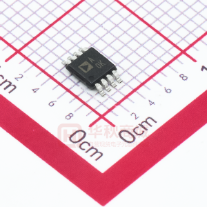
引脚分配: - AD8615:5引脚TSOT-23封装。 - AD8616:8引脚MSOP和窄SOIC表面贴装封装。 - AD8618:14引脚SOIC和TSSOP封装。

参数特性: - 低失调电压:最大65μV。 - 单电源运行:2.7 V至5.5 V。 - 低噪声:8 nV/√Hz。 - 宽带宽:大于20 MHz。 - slew rate(斜率):12 V/μs。 - 高输出电流:150 mA。 - 无相位反转。 - 低输入偏置电流:1 pA。 - 低供电电流:2 mA。 - 增益为1时稳定。

功能详解: - 这些放大器因其20 MHz的带宽、低失调、低噪声和非常低的输入偏置电流,在多种应用中非常有用。 - 它们适用于滤波器、积分器、光电二极管放大器和高阻抗传感器等多种应用。 - AC应用受益于宽带宽和低失真。 - AD8615/AD8616/AD8618提供DigiTrim™家族中最高的输出驱动能力,非常适合音频线驱动器和其他低阻抗应用。

应用信息: - 便携式和低功耗仪器、便携式设备的音频放大、手机耳机、条码扫描器和多极滤波器等应用。 - 设计师可以利用其在单电源系统中缓冲CMOS ADC、DAC、ASIC等宽输出摆动设备的能力。

封装信息: - 提供了不同封装类型的热阻数据,包括TSOT-23、MSOP、SOIC和TSSOP。 - 详细图纸展示了不同封装的尺寸和控制尺寸。
AD8616ARMZ-R21 价格&库存

很抱歉,暂时无法提供与“AD8616ARMZ-R21”相匹配的价格&库存,您可以联系我们找货

免费人工找货
AD8616ARMZ-REEL
  •  国内价格
  • 1+27.12

库存:106