a
FEATURES
PRELIMINARY TECHNICAL DATA Zero-Drift, Single-Supply, Rail-to-Rail Input/Output Low Noise Operational Amplifier
Preliminary Technical Data
Lowest auto-zero amplifier noise Low Offset Voltage: 5 µV Input Offset Drift: 0.03 µV/°C Rail-to-Rail Input and Output Swing 5 V Single-Supply Operation High Gain, CMRR, and PSRR: 120 dB Very Low Input Bias Current: 100 pA Low Supply Current: 1.3 mA Overload Recovery Time: 0.2 ms No External Components Required
AD8628
the AD8628 family to reduce input biasing complexity and maximize SNR. The AD8628 family is specified for the extended industrial (-40° to +125°C) temperature range. The AD8628 amplifier is available in the tiny SOT23 and the popular 8-pin narrow SOIC plastic packages.
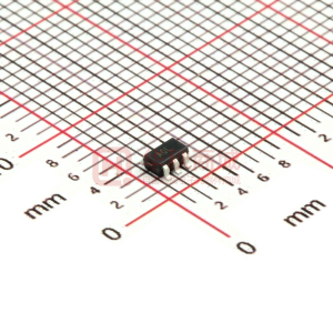
5-Lead SOT (RT-5)
APPLICATIONS
Automotive Sensors Pressure and Position Sensors Strain Gage Amplifiers Medical Instrumentation Thermocouple Amplifiers
AD8628
8-Lead SO (R-8)
GENERAL DESCRIPTION
This new family of amplifiers has ultra-low offset, drift and bias current. The AD8628 is a wide bandwidth auto-zero amplifier featuring rail-to-rail input and output swings and low noise. Operation is fully specified from 2.7 to 5 volts single supply (±1.35V to ±2.5V dual supply). The AD8628 family provides the benefits previously found only in expensive auto-zeroing or chopper-stabilized amplifiers. Using Analog Devices’ new topology these zero-drift amplifiers combine low cost, with high accuracy and low noise. (No external capacitors are required.) In addition, the AD8628 greatly reduces the digital switching noise found in most chopper stabilized amplifiers. With an offset voltage of only 1µV, drift less than 0.005 µV/°C and noise of only 0.5uV P-P (0Hz to 10 Hz) the AD8628 is perfectly suited for applications where error sources cannot be tolerated. Position and pressure sensors, medical equipment, and strain gage amplifiers benefit greatly from nearly zero drift over their operating temperature range. Many systems may take advantage of the rail-to-rail input and output swings provided by
AD8628
Specifications
Information furnished by Analog Devices is believed to be accurate and reliable. However, no responsibility is assumed by Analog Devices for its use, nor for any infringements of patents or other rights of third parties which may result from its use. No license is granted by implication or otherwise under any patent or patent rights of Analog Devices. O ne Technology Way, P.O. Box 9106, Norwood, MA 02062-9106, U.S.A. World Wide Web Site: http://www.analog.com Tel: 617/329-4700 © Analog Devices, Inc., 2002 Fax: 617/326-8703
�PRELIMINARY TECHNICAL DATA
AD8628
ELECTRICAL SPECIFICATIONS (@ VS=+5.0V, VCM = +2.5V, VO=+2.5V, TA=+25°C unless otherwise specified.)
Parameter INPUT CHARACTERISTICS Offset Voltage Input Bias Current Input Offset Current Input Voltage Range Common-Mode Rejection Ratio Large Signal Voltage Gain (Note 1) Offset Voltage Drift OUTPUT CHARACTERISTICS Output Voltage High Symbol VOS -40°C ≤ TA ≤ +125°C IB -40°C ≤ TA ≤ +125°C IOS -40°C ≤ TA ≤ +125°C CMRR AVO ∆VOS/∆T VOH VCM = 0V to 5V -40°C ≤ TA ≤ +125°C RL = 10 kΩ, Vo=0.3 to 4.7V -40°C ≤ TA ≤ +125°C -40°C ≤ TA ≤ +125°C RL = 100kΩ to Ground -40°C ≤ TA ≤ +125°C RL = 10kΩ to Ground -40°C ≤ TA ≤ +125°C Output Voltage Low VOL RL = 100kΩ to V+ -40°C ≤ TA ≤ +125°C RL = 10 kΩ to V+ -40°C ≤ TA ≤ +125°C Short Circuit Limit Output Current POWER SUPPLY Power Supply Rejection Ratio Supply Current/Amplifier DYNAMIC PERFORMANCE Slew Rate Overload Recovery Time Gain Bandwidth Product NOISE PERFORMANCE Voltage Noise Voltage Noise Voltage Noise Density Current Noise Density ISC -40°C ≤ TA ≤ +125°C IO -40°C ≤ TA ≤ +125°C PSRR ISY VS = 2.7V to 5.5V -40°C ≤ TA ≤ +125°C V O = 0V -40°C ≤ TA ≤ +125°C SR GBP en p-p en p-p en in 0.1 to 10 Hz 0.1 to 1.0 Hz f = 1 kHz f=10 Hz RL =10 kΩ 120 115 ± 25 4.99 4.99 4.95 4.95 0 120 115 125 120 140 130 145 135 0.002 4.996 4.995 4.98 4.97 1 2 10 15 ± 50 ± 40 ± 30 ± 15 130 130 1.3 1.6 0.8 0.05 2.5 0.5 0.16 22 5 1.5 1.8 10 10 20 20 0.03 50 30 Conditions Min Typ 1 Max 5 10 100 1.5 200 250 5 Units µV µV pA nA pA pA V dB dB dB dB µV/°C V V V V mV mV mV mV mA mA mA mA dB dB mA mA V/µs ms MHz µVp-p µVp-p nV/√Hz fA/√Hz
0.2
Note 1: Gain testing is highly dependent upon test bandwidth.
–2–
REV. PrA
1/29/02
�PRELIMINARY TECHNICAL DATA
AD8628
ELECTRICAL SPECIFICATIONS (@ VS=+2.7V, VCM = +1.35 V, VO=1.4V, TA=+25°C unless otherwise specified.)
Parameter INPUT CHARACTERISTICS Offset Voltage AD8628 Input Bias Current Input Offset Current Input Voltage Range Common-Mode Rejection Ratio Large Signal Voltage Gain Offset Voltage Drift OUTPUT CHARACTERISTICS Output Voltage High Symbol VOS -40°C ≤ TA ≤ +125°C IB -40°C ≤ TA ≤ +125°C IOS -40°C ≤ TA ≤ +125°C CMRR AVO ∆VOS/∆T VOH VCM = 0 to 2.9V -40°C ≤ TA ≤ +125°C RL = 10 kΩ, Vo=0.3 to 4.7V -40°C ≤ TA ≤ +125°C -40°C ≤ TA ≤ +125°C RL = 100kΩ to Ground -40°C ≤ TA ≤ +125°C RL = 10kΩ to Ground -40°C ≤ TA ≤ +125°C Output Voltage Low VOL RL = 100kΩ to V+ -40°C ≤ TA ≤ +125°C RL = 10 kΩ to V+ -40°C ≤ TA ≤ +125°C Short Circuit Limit Output Current POWER SUPPLY Power Supply Rejection Ratio Supply Current/Amplifier DYNAMIC PERFORMANCE Slew Rate Overload Recovery Time Gain Bandwidth Product NOISE PERFORMANCE Voltage Noise Voltage Noise Density Current Noise Density ISC -40°C ≤ TA ≤ +125°C IO -40°C ≤ TA ≤ +125°C PSRR ISY VS = 2.7V to 5.5 V -40°C ≤ TA ≤ +125°C V O = 0V -40°C ≤ TA ≤ +125°C SR GBP en p-p en in 0.1 to 10 Hz f = 1 kHz f=10 Hz RL =10 kΩ 120 115 ±10 2.68 2.68 2.67 2.67 0 115 110 110 105 130 120 140 130 0.002 2.695 2.695 2.68 2.675 1 2 10 15 ± 15 ± 10 ± 10 ±5 130 130 1.1 1.3 1 0.05 2 0.75 33 5 1.4 1.6 10 10 20 20 0.03 30 1.0 50 Conditions Min Typ 1 Max 5 10 100 1.5 200 250 5 Units µV µV pA nA pA pA V dB dB dB dB µV/°C V V V V mV mV mV mV mA mA mA mA dB dB mA mA V/µs ms MHz µVp-p nV/√Hz fA/√Hz
Specifications
–3–
�PRELIMINARY TECHNICAL DATA
AD8628
ABSOLUTE MAXIMUM RATINGS Supply Voltage ..........................................................................+6V Input Voltage......................................................GND to Vs + 0.3V Differential Input Voltage1 .....................................................±5.0V Output Short-Circuit Duration to Gnd...............................Indefinite Storage Temperature Range RT, R Package ............................................... -65°C to +150°C Operating Temperature Range AD8628 ......................................................... -40°C to +125°C Junction Temperature Range RT, R Package ............................................... -65°C to +150°C Lead Temperature Range (Soldering, 10 sec).......................+300°C Package Type 5-Pin SOT23 (RT) 8-Pin SOIC (R) NOTES
1 Differential input voltage is limited to ±5.0 volts or the supply voltage, whichever is less. 2 θ is specified for the worst case conditions, i.e., θ is specified for device in socket JA JA for P-DIP packages; θJAis specified for device soldered in circuit board for SOIC and TSSOP packages.
θJA2 158
θJC 43
Units °C/W °C/W
ORDERING GUIDE Model AD8628ART AD8628AR Temperature Range -40°C to +125°C -40°C to +125°C Package Description 5-Pin SOT23 8-Pin SOIC Package Option RT-5 SO-8
–4–
REV. PrA
1/29/02
�
很抱歉,暂时无法提供与“AD8628ART”相匹配的价格&库存,您可以联系我们找货
免费人工找货


 工商网监
湘ICP备2023018690号
工商网监
湘ICP备2023018690号