Dual Precision, Rail-to-Rail Output
Operational Amplifier
AD8698
FEATURES
CONNECTION DIAGRAMS
OUT A 1
–IN A 2
+IN A 3
AD8698
8-Lead MSOP
(RM-8)
8
V+
7
OUT B
6 –IN B
TOP VIEW
V– 4 (Not to Scale) 5 +IN B
OUT A 1
–IN A 2
+IN A 3
AD8698
8
V+
7
OUT B
6 –IN B
TOP VIEW
V– 4 (Not to Scale) 5 +IN B
04807-0-070
8-Lead SOIC
(R-8)
04807-0-069
Low offset voltage: 100 µV max
Low offset voltage drift: 2 µV/°C max
Low input bias current: 700 pA max
Low noise: 8 nV/√Hz
High common-mode rejection: 118 dB min
Wide operating temperature: −40°C to +85°C
No phase reversal
Figure 1.
APPLICATIONS
Photodiode amplifier
Sensors and controls
Multipole filters
Integrator
GENERAL DESCRIPTION
The AD8698 is a high precision, rail-to-rail output, low noise,
low input bias current operational amplifier. Offset voltage is a
respectable 100 µV max and drift over temperature is below
2 µV/°C, eliminating the need for manual offset trimming. The
AD8698 is ideal for high impedance sensors, minimizing offset
errors due to input bias and offset currents.
The rail-to-rail output maximizes dynamic range in a variety of
applications, such as photodiode amplifiers, DAC I/V
amplifiers, filters, and ADC input amplifiers.
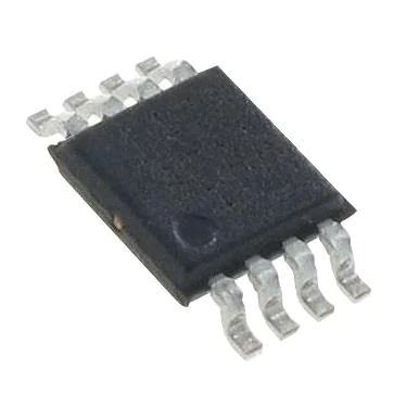
The AD8698 dual amplifiers are offered in 8-lead MSOP and
narrow 8-lead SOIC packages. The MSOP version is available
in tape and reel only.
Rev. 0
Information furnished by Analog Devices is believed to be accurate and reliable.
However, no responsibility is assumed by Analog Devices for its use, nor for any
infringements of patents or other rights of third parties that may result from its use.
Specifications subject to change without notice. No license is granted by implication
or otherwise under any patent or patent rights of Analog Devices. Trademarks and
registered trademarks are the property of their respective owners.
One Technology Way, P.O. Box 9106, Norwood, MA 02062-9106, U.S.A.
Tel: 781.329.4700
www.analog.com
Fax: 781.326.8703
© 2004 Analog Devices, Inc. All rights reserved.
�AD8698
TABLE OF CONTENTS
Specifications .................................................................................... 3
Instrumentation Amplifier ....................................................... 15
Absolute Maximum Ratings ........................................................... 5
Composite Amplifier ................................................................. 15
Thermal Resistance ...................................................................... 5
Low Noise Applications ............................................................ 16
ESD Caution.................................................................................. 5
Driving ADCs ............................................................................. 16
Typical Performance Characteristics............................................. 6
Using the AD8698 in Active Filter Designs ........................... 16
Applications .................................................................................... 14
Outline Dimensions....................................................................... 17
Input Overvoltage Protection................................................... 14
Ordering Guide .......................................................................... 17
Driving Capacitive Loads .......................................................... 14
REVISION HISTORY
4/04—Revision 0: Initial Version
Rev. 0 | Page 2 of 20
�AD8698
SPECIFICATIONS
VS = ±15 V, VCM = 0 V (@TA = 25oC, unless otherwise noted.)
Table 1.
Parameter
Symbol
Conditions
Min
Typ
Max
Unit
20
100
300
µV
µV
INPUT CHARACTERISTICS
Offset Voltage
VOS
Offset Voltage Drift
Input Bias Current
∆VOS/∆T
IB
Input Offset Current
IOS
Input Voltage Range
Common-Mode Rejection Ratio
Large Signal Voltage Gain
Input Capacitance
IVR
CMRR
AVO
CDIFF
CCM
−40°C < TA < +85°C
−40°C < TA < +85°C
0.6
−40°C < TA < +85°C
OUTPUT CHARACTERISTICS
Output Voltage Swing
(Ref. to GND)
(Ref. to GND)
POWER SUPPLY
Power Supply Rejection Ratio
Supply Current
Supply Voltage
DYNAMIC PERFORMANCE
Slew Rate
132
1450
6.5
4.6
VOH
IL = 1 mA, −40°C < TA < +85°C
14.85
14.93
V
IL = 5 mA, −40°C < TA < +85°C
14.6
14.8
V
VOL
IL = 1 mA, −40°C < TA < +85°C
−14.93
−14.6
V
VOL
IL = 5 mA, −40°C < TA < +85°C
−14.82
−14.5
V
PSRR
ISY
±2.5 V < VS < ±15 V
VO = 0 V
VS
−40°C < TA < +85°C
−40°C < TA < +85°C
3.2
3.8
±15
dB
mA
mA
V
SR
RL = 2 kΩ
GBP
Phase Margin
ØO
Input Voltage Noise Density
RL = 2 kΩ, VO = ±13.5 V
−13.5V
118
900
µV/°C
pA
pA
pA
pA
V
dB
V/mV
pF
pF
VOH
Gain Bandwidth Product
NOISE PERFORMANCE
Input Noise Voltage
−40°C < TA < +85°C
−40°C < TA < +85°C
VCM = ±13.5 V
2
700
1500
700
1500
13.5
114
132
2.8
±2.5
0.4
V/µs
1
MHz
60
Degrees
en p-p
0.1 Hz < f < 10 Hz
0.6
µV p-p
en
f = 10 Hz
15
nV/√Hz
Input Voltage Noise Density
en
f = 1 kHz
8
nV/√Hz
Current Noise Density
in
f = 1 kHz
0.2
pA/√Hz
Rev. 0 | Page 3 of 20
�AD8698
VS = ±2.5 V, VCM = 0 V (@TA = 25oC, unless otherwise noted.)
Table 2.
Parameter
Symbol
Conditions
Min
Typ
Max
Unit
20
100
µV
INPUT CHARACTERISTICS
Offset Voltage
VOS
Offset Voltage Drift
Input Bias Current
∆VOS/∆T
IB
Input Offset Current
IOS
−40°C < TA < +85°C
300
µV
−40°C < TA < +85°C
2
µV/°C
700
1500
700
1500
+1.5
120
1200
6.4
4.6
pA
pA
pA
pA
V
dB
V/mV
pF
pF
2.44
2.29
V
V
−40°C < TA < +85°C
Input Voltage Range
Common-Mode Rejection Ratio
Large Signal Voltage Gain
Input Capacitance
OUTPUT CHARACTERISTICS
Output Voltage Swing
(Ref. to GND)
(Ref. to GND)
IVR
CMRR
AVO
CDIFF
CCM
VOH
VOH
−40°C < TA < +85°C
−40°C < TA < +85°C
VCM = ±13.5 V
RL = 2 kΩ, VO = ±13.5 V
−1.5
105
600
IL = 1 mA, −40°C < TA < +85°C
IL = 5 mA, −40°C < TA < +85°C
2.35
2.1
VOL
IL = 1 mA, −40°C < TA < +85°C
−2.43
−2.2
V
VOL
IL = 5 mA, TA = 25°C
−2.15
−1.9
V
IL= 5mA, −40°C
很抱歉,暂时无法提供与“AD8698ARM-R2”相匹配的价格&库存,您可以联系我们找货
免费人工找货