a
FEATURES 200 MSPS Guaranteed Conversion Rate 135 MSPS Low Cost Version Available 350 MHz Analog Bandwidth 1 V p-p Analog Input Range Internal +2.5 V Reference and T/H Low Power: 500 mW +5 V Single Supply Operation TTL Output Interface Single or Demultiplexed Output Ports APPLICATIONS RGB Graphics Processing High Resolution Video Digital Data Storage Read Channels Digital Communications Digital Instrumentation Medical Imaging
VREF IN
8-Bit, 200 MSPS A/D Converter AD9054A
FUNCTIONAL BLOCK DIAGRAM
VREF OUT
AD9054A
AIN AIN ENCODE ENCODE T/H QUANTIZER
2.5V REFERENCE 8 ENCODE LOGIC 8 DEMULTIPLEXER
DA7 –DA0 DB7 –DB0
TIMING
VDD
GND
DEMUX
DS
DS
GENERAL DESCRIPTION
The AD9054A is an 8-bit monolithic analog-to-digital converter optimized for high speed, low power, small size and ease of use. With a 200 MSPS encode rate capability and full-power analog bandwidth of 350 MHz, the component is ideal for applications requiring the highest possible dynamic performance. To minimize system cost and power dissipation, the AD9054A includes an internal +2.5 V reference and track-and-hold circuit. The user provides only a +5 V power supply and an encode clock. No external reference or driver components are required for many applications.
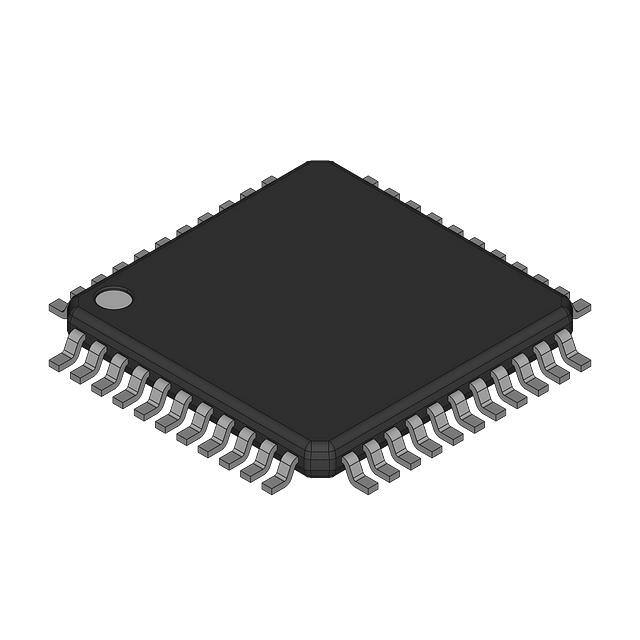
The AD9054A’s encode input interfaces directly to TTL, CMOS or positive-ECL logic and will operate with single-ended or differential inputs. The user may select dual-channel or singlechannel digital outputs. The dual (demultiplexed) mode interleaves ADC data through two 8-bit channels at one-half the clock rate. Operation in demultiplexed mode reduces the speed and cost of external digital interfaces while allowing the ADC to be clocked to the full 200 MSPS conversion rate. In the singlechannel (nondemultiplexed) mode, all data is piped at the full clock rate to the Channel A outputs. Fabricated with an advanced BiCMOS process, the AD9054A is provided in a space-saving 44-lead LQFP surface mount plastic package (ST-44) and specified over the full industrial (–40°C to +85°C) temperature range.
R EV. B
Information furnished by Analog Devices is believed to be accurate and reliable. However, no responsibility is assumed by Analog Devices for its use, nor for any infringements of patents or other rights of third parties which may result from its use. No license is granted by implication or otherwise under any patent or patent rights of Analog Devices. One Technology Way, P.O. Box 9106, Norwood, MA 02062-9106, U.S.A. Tel: 781/329-4700 World Wide Web Site: http://www.analog.com Fax: 781/326-8703 © Analog Devices, Inc., 2000
�AD9054A–SPECIFICATIONS
ELECTRICAL CHARACTERISTICS (V
Parameter RESOLUTION DC ACCURACY Differential Nonlinearity Integral Nonlinearity No Missing Codes Gain Error1 Gain Tempco1 ANALOG INPUT Input Voltage Range (With Respect to AIN) Compliance Range AIN or AIN Input Offset Voltage Input Resistance Input Capacitance Input Bias Current Analog Bandwidth, Full Power 2 REFERENCE OUTPUT Output Voltage Temperature Coefficient SWITCHING PERFORMANCE Maximum Conversion Rate (f S) Minimum Conversion Rate (f S) Encode Pulsewidth High (t EH) Encode Pulsewidth Low (t EL) Aperture Delay (tA) Aperture Uncertainty (Jitter) Data Sync Setup Time (t SDS) Data Sync Hold Time (t HDS) Data Sync Pulsewidth (t PWDS) Output Valid Time (t V)3 Output Propagation Delay (t PD)3 DIGITAL INPUTS HIGH Level Current (I IH)4 LOW Level Current (I IL)4 Input Capacitance DIFFERENTIAL INPUTS Differential Signal Amplitude (VID) HIGH Input Voltage (V IHD) LOW Input Voltage (V ILD) Common-Mode Input (V ICM) DEMUX INPUT HIGH Input Voltage (V IH) LOW Input Voltage (V IL) DIGITAL OUTPUTS HIGH Output Voltage (V OH) LOW Output Voltage (V OL) Output Coding +25°C Full +25°C Full Full +25°C Full I VI I VI VI I V Temp
DD
= +5 V, external reference, fS = max unless otherwise noted)
Test Level AD9054ABST-200 Min Typ Max 8 ± 0.9 ± 1.0 ± 0.6 ± 0.9 Guaranteed ±2 160 +1.5/–1.0 +2.0/–1.0 ± 1.5 ± 2.0 ±7 AD9054ABST-135 Min Typ Max 8 ± 0.9 ± 1.0 ± 0.6 ± 0.9 Guaranteed ±2 160 +1.5/–1.0 +2.0/–1.0 ± 1.5 ± 2.0 ±7 Unit Bits LSB LSB LSB LSB % FS ppm/°C
Full Full +25°C Full +25°C Full +25°C +25°C Full +25°C Full Full Full Full +25°C +25°C +25°C +25°C +25°C +25°C +25°C Full Full Full Full +25°C Full Full Full Full Full Full Full Full
V V I VI I VI V I VI V VI V VI IV IV IV V V IV IV IV VI VI VI VI V IV IV IV IV IV IV VI VI
± 512 1.8 ±4 ±8 62 4 25 350 2.4 2.5 110 2.6 2.4 3.2 ± 16 ± 19 1.8
± 512 ±4 ±8 62 4 25 350 2.5 110 2.6 3.2 ± 16 ± 19
36 23
36 23 50 75
50 75
mV p-p V mV mV kΩ kΩ pF µA µA MHz V ppm/°C MSPS MSPS ns ns ns ps rms ns ns ns ns ns µA µA pF mV V V V V V V V
200 2.0 2.0 0.5 2.3 0 0.5 2.0 2.7 25 22 22
135 3.0 3.0 0.5 2.3 0 0.5 2.0 2.7 7.9 625 625 25 22 22
5.1 5.9 500 500 3
5.7 7.5 500 500 3
8.5 625 625
400 1.5 0 1.5 2.0 0 2.4
VDD VDD – 0.4
400 1.5 0 1.5 2.0 0 2.4
VDD VDD – 0.4
VDD 0.8
VDD 0.8
0.4 Binary Binary
0.4
– 2–
REV. B
�AD9054A
Parameter POWER SUPPLY VDD Supply Current (IDD) Power Dissipation5, 6 Power Supply Sensitivity 7 DYNAMIC PERFORMANCE 8 Transient Response Overvoltage Recovery Time Signal-to-Noise Ratio (SNR) (Without Harmonics) fIN = 19.7 MHz fIN = 49.7 MHz fIN = 70.1 MHz Signal-to-Noise Ratio (SINAD) (With Harmonics) fIN = 19.7 MHz fIN = 49.7 MHz fIN = 70.1 MHz Effective Number of Bits fIN = 19.7 MHz fIN = 49.7 MHz fIN = 70.1 MHz 2nd Harmonic Distortion fIN = 19.7 MHz fIN = 49.7 MHz fIN = 70.1 MHz 3rd Harmonic Distortion fIN = 19.7 MHz fIN = 49.7 MHz fIN = 70.1 MHz Two-Tone Intermod Distortion (IMD) fIN = 19.7 MHz fIN = 49.7 MHz fIN = 70.1 MHz Temp Full Full +25°C +25°C +25°C +25°C Full +25°C Full +25°C Full Test Level VI VI I V V AD9054ABST-200 Min Typ Max 128 640 0.005 1.5 1.5 145 725 0.015 AD9054ABST-135 Min Typ Max 120 600 0.005 1.5 1.5 140 700 0.015 Unit mA mW V/V ns ns
IV V I V I V
42 42 42
45 45 45 45 45 45
42 42
45 45 45 45
dB dB dB dB dB dB
+25°C Full +25°C Full +25°C Full +25°C +25°C +25°C +25°C +25°C +25°C +25°C +25°C +25°C +25°C +25°C +25°C
IV V I V I V IV I I IV I I IV I I
40 40 39
43 43 43 43 42 42 6.85 6.85 6.85 63 59 55 56 54 50
40 40
43 43 43 43
dB dB dB dB dB dB Bits Bits Bits dBc dBc dBc dBc dBc dBc
6.35 6.35 6.18 58 54 49 48 48 43
6.35 6.35
6.85 6.85
58 54
63 59
48 48
56 54
V V V
60 55 50
60 55
dBc dBc dBc
NOTES 1 Gain error and gain temperature coefficient are based on the ADC only (with a fixed +2.5 V external reference). 2 3 dB bandwidth with full-power input signal. 3 tV and tPD are measured from the threshold crossing of the ENCODE input to valid TTL levels of the digital outputs. The output ac load during test is 5 pF (Refer to equivalent circuits Figures 5 and 6). 4 IIH and IIL are valid for differential input voltages of less than 1.5 V. At higher differential voltages, the input current will increase to a maximum of 1.5 mA. 5 Power dissipation is measured under the following conditions: analog input is –1 dBFS at 19.7 MHz. 6 Typical thermal impedance for the ST-44 (LQFP) 44-lead package (in still air): θJC = 20°C/W, θCA = 35°C/W, θJA = 55°C/W. 7 A change in input offset voltage with respect to a change in V DD. 8 SNR/harmonics based on an analog input voltage of –1.0 dBFS referenced to a 1.024 V full-scale input range. Specifications subject to change without notice.
EXPLANATION OF TEST LEVELS Test Level
IV. Parameter is guaranteed by design and characterization testing. V. Parameter is a typical value only. VI. 100% production tested at +25°C; guaranteed by design and characterization testing for industrial temperature range.
I. 100% production tested. II. 100% production tested at +25°C and sample tested at specified temperatures. III. Sample tested only.
REV. B
– 3–
�AD9054A
ABSOLUTE MAXIMUM RATINGS* Table I. Output Coding
VDD . . . . . . . . . . . . . . . . . . . . . . . . . . . . . . . . . . . . . . . . +6 V Analog Inputs . . . . . . . . . . . . . . . . . . . . . . . . . . VDD to 0.0 V Digital Inputs . . . . . . . . . . . . . . . . . . . . . . . . . . VDD to 0.0 V VREF IN, VREF OUT . . . . . . . . . . . . . . . . . . . VDD to 0.0 V Digital Output Current . . . . . . . . . . . . . . . . . . . . . . . . 20 mA Operating Temperature . . . . . . . . . . . . . . . . –55°C to +125°C Storage Temperature . . . . . . . . . . . . . . . . . . –65°C to +150°C Maximum Junction Temperature . . . . . . . . . . . . . . . +175°C Maximum Case Temperature . . . . . . . . . . . . . . . . . . +150°C
*Stresses above those listed under Absolute Maximum Ratings may cause permanent damage to the device. This is a stress rating only; functional operation of the device at these or any other conditions outside of those indicated in the operation sections of this specification is not implied. Exposure to absolute maximum ratings for extended periods may affect device reliability.
Step 255 254 253 • • • 129 128 127 126 • • • 2 1 0
AIN–AIN ≥0.512 V 0.508 V 0.504 V • • • 0.006 V 0.002 V –0.002 V –0.006 V • • • –0.504 V –0.508 V ≤–0.512 V
Code 255 254 253 • • • 129 128 127 126 • • • 2 1 0
Binary 1111 1111 1111 1110 1111 1101 • • • 1000 0001 1000 0000 0111 1111 0111 1110 • • • 0000 0010 0000 0001 0000 0000
ORDERING GUIDE
Model AD9054ABST-200 AD9054ABST-135 AD9054A/PCB
Temperature Range –40°C to +85°C –40°C to +85°C +25°C
Package Option* ST-44 ST-44 Evaluation Board
*ST = Plastic Thin Quad Flatpack (LQFP).
CAUTION ESD (electrostatic discharge) sensitive device. Electrostatic charges as high as 4000 V readily accumulate on the human body and test equipment and can discharge without detection. Although the AD9054A features proprietary ESD protection circuitry, permanent damage may occur on devices subjected to high-energy electrostatic discharges. Therefore, proper ESD precautions are recommended to avoid performance degradation or loss of functionality.
WARNING!
ESD SENSITIVE DEVICE
–4–
REV. B
�AD9054A
PIN FUNCTION DESCRIPTIONS Pin Number 1 Name ENCODE Function Encode Clock for ADC (ADC Samples on Rising Edge of ENCODE). Encode Clock Complement (ADC Samples on Falling Edge of ENCODE). Power Supply (+5 V). Ground.
VREF OUT
PIN CONFIGURATION
DB7 (MSB)
GND
GND
GND
VDD
VDD
VDD
DB6
DB5
DB4
2
ENCODE
VREF IN GND VDD GND AIN AIN GND VDD DEMUX DS DS
PIN 1 IDENTIFIER
DB3 DB2 DB1 DB0 (LSB)
3, 5, 15, 18, 28, VDD 30, 31, 36, 41 4, 6, 16, 17, 27, GND 29, 32, 35, 37, 40 14–7 DA0–DA7 19–26 33
AD9054A
TOP VIEW (PINS DOWN)
VDD GND GND VDD DA0 (LSB) DA1 DA2
34 38
39 42
43 44
Digital Outputs of ADC Channel A. DA7 is the MSB, DA0 the LSB. DB0–DB7 Digital Outputs of ADC Channel B. DB7 is the MSB, DB0 the LSB. VREF OUT Internal Reference Output (+2.5 V typical); Bypass with 0.1 µF to Ground. VREF IN Reference Input for ADC (+2.5 V typical, ± 4%). AIN Analog Input—Complement. Connect to input signal midscale reference. AIN Analog Input—True. DEMUX Format Select. LOW = Dual. Channel Mode, HIGH = Single. Channel Mode (Channel A Only). DS Data Sync Complement. DS Data Sync—Aligns output channels in Dual-Channel Mode.
VDD
ENCODE
ENCODE
GND
VDD
DA7 (MSB)
GND
DA6
DA5
DA4
SAMPLE N–1
SAMPLE N
SAMPLE N+3
SAMPLE N+4
AIN
SAMPLE N+1 SAMPLE N+2
tA tEH ENCODE tEL
1/fS
ENCODE tPD
DA3
tV
D7 – D 0
DATA N–5
DATA N–4
DATA N–3
DATA N–2
DATA N–1
DATA N
Figure 1. Timing—Single Channel Mode
REV. B
–5–
�AD9054A
SAMPLE N–1 SAMPLE N SAMPLE N+3 SAMPLE N+4 SAMPLE N+5
AIN
SAMPLE N–2 SAMPLE N+1 1/fS SAMPLE N+2 SAMPLE N+6
tA tEH tEL
ENCODE ENCODE tHDS tSDS DS DS tPWDS PORT A D7 – D 0
DATA N–7 OR N–8
tHDS tSDS
tPD
DATA N–7 OR N–6 INVALID IF OUT OF SYNC DATA N–4 IF IN SYNC
tV
DATA N–2
DATA N
PORT B D7 – D 0
DATA N–8 OR N–7
DATA N–6 OR N–7
INVALID IF OUT OF SYNC DATA N–5 IF IN SYNC
DATA N–3
DATA N–1
DATA N+1
Figure 2a. Timing—Dual Channel Mode (One-Shot Data Sync)
SAMPLE N–1
SAMPLE N
SAMPLE N+3
SAMPLE N+4
SAMPLE N+5
AIN
SAMPLE N–2 SAMPLE N+1 1/fS SAMPLE N+2 SAMPLE N+6
tA tEH tEL
ENCODE ENCODE tHDS DS DS tPWDS tSDS tHDS
tSDS
tPD
DATA N–7 OR N–6 INVALID IF OUT OF SYNC DATA N–4 IF IN SYNC
tV
PORT A D7 – D 0
DATA N–7 OR N–8
DATA N–2
DATA N
PORT B D7 – D 0
DATA N–8 OR N–7
DATA N–6 OR N–7
INVALID IF OUT OF SYNC DATA N–5 IF IN SYNC
DATA N–3
DATA N–1
DATA N+1
Figure 2b. Timing—Dual Channel Mode (Continuous Data Sync)
–6–
REV. B
�AD9054A
EQUIVALENT CIRCUITS
VDD
300 17.5k DEMUX 300 VDD
AIN
AIN
7.5k
Figure 3. Equivalent Analog Input Circuit
Figure 6. Equivalent DEMUX Input Circuit
VDD
VDD
VREF IN
DIGITAL OUTPUTS
Figure 4. Equivalent Reference Input Circuit
Figure 7. Equivalent Digital Output Circuit
VDD
VDD 17.5k ENCODE OR DS 300 300 ENCODE OR DS
VREF OUT
7.5k
Figure 5. Equivalent ENCODE and Data Select Input Circuit
Figure 8. Equivalent Reference Output Circuit
REV. B
–7–
�AD9054A
55 45.4 45.2 50 SNR SNR – dB SNR – dB 45 SINAD 40 NYQUIST FREQUENCY (100MHz) 45.0 50MHz 44.8 44.6 70MHz 44.4 44.2 44.0 –45 20MHz
35
30
0
20
40
60 80 fIN – MHz
100
120
140
0
25 TC – C
70
90
Figure 9. SNR vs. fIN: fS = 200 MSPS
Figure 12. SNR vs. Temperature, fS = 135 MSPS
50 49 48 47
46.0 45.8 45.6 20MHz 45.4 50MHz
SNR – dB
SNR – dB
46 45 44 43 42 41 40 25 50 75 100 125 150 175 200 225 250 270 fS – MSPS 300 SNR
45.2 45.0 44.8 44.6 44.4 44.2 44.0 –60 –40 –20 0 20 TC – C 40 60 80 100 70MHz
SINAD
Figure 10. SNR vs. fS: fIN = 19.7 MHz
Figure 13. SNR vs. Temperature, fS = 200 MSPS
50 SNR
50 48 46
SINAD
45
fS = 135MSPS fIN = 10.3MHz
40
44
SNR – dB
SNR – dB
42 SNR 40 38 SINAD 36 34 32
35
30
25
20 25
50
75
100 125 150 175 200 225 250 270 300 fS – MSPS
30 0.0
1.0
2.0
3.0 4.0 5.0 6.0 ENCODE PULSEWIDTH – ns
7.0
8.0
Figure 11. SNR vs. fS: fIN = 70.1 MHz
Figure 14. SNR vs. Clock Pulsewidth, (tPWH): fS = 135 MSPS
–8–
REV. B
�AD9054A
50 48 46
–64 –70
fS = 200MSPS fIN = 10.3MHz
–68
2ND HARMONIC
SNR
–66
44 SINAD
SNR – dB
–62 –60
42
dBc
40 38 36 34 32 30 0.0 0.5 1.0 1.5 2.0 2.5 3.0 3.5 4.0 ENCODE PULSEWIDTH – ns 4.5 5.0
–58 –56 –54 –52 –50 –48 –46 25 50 75
3RD HARMONIC
100 125 150 175 200 225 250 fS – MSPS
270 300
Figure 15. SNR vs. Clock Pulsewidth, (tPWH): fS = 200 MSPS
Figure 18. Harmonic Distortion vs. fS: fIN = 19.7 MHz
46 45 44 20MHz
–60
2ND HARMONIC
–50
–40 3RD HARMONIC
SINAD – dB
43 42 41 40 –10 39 38 –60 0 25 70MHz 50MHz –20 –30
–40
–20
0
20 40 TC – C
60
80
100
50
75
100 125
150 175
200 225 250 270 300
fS – MSPS
Figure 16. SINAD vs. Temperature: fS = 135 MSPS
Figure 19. Harmonic Distortion vs. fS: fIN = 70.1 MHz
46 45 44 20MHz
–40
–45
–50
SINAD – dB
43 50MHz
dB
42 70MHz 41 40
–55 70MHz –60 50MHz –65 20MHz
39 38 –60
–40
–20
0
20 TC – C
40
60
80
100
–70 –60
–40
–20
0
20 TC – C
40
60
80
100
Figure 17. SINAD vs. Temperature: fS = 200 MSPS
Figure 20. 2nd Harmonic vs. Temperature: fS = 135 MSPS
REV. B
–9–
�AD9054A
–40 0 –45 –1
–50 70MHz dB –55 50MHz –60 20MHz –65 dB
–2
–3
–4 NYQUIST FREQUENCY 100MHz –5
–70 –60
–40
–20
0
20 TC – C
40
60
80
100
–6 0 50 100 150 200 250 300 fIN – M Hz 350 400 450 500
Figure 21. 2nd Harmonic vs. Temperature: fS = 200 MSPS
Figure 24. Frequency Response: fS = 200 MSPS
–40
0 –10 FUNDAMENTAL = –0.5dBFS SNR = 45.8dB SINAD = 45.2dB 2ND HARMONIC = 69.8dB 3RD HARMONIC = 61.6dB
–45 –20 –50 70MHz 50MHz –30 –40
dB
dB
–55 20MHz –60
–50 –60 –70
–65 –80 –70 –60 –40 –20 0 20 TC – C 40 60 80 100 –90 0
10
20
30
40
50 60 MHz
70
80
90
100
Figure 22. 3rd Harmonic vs. Temperature: fS = 135 MSPS
Figure 25. Spectrum: fS = 200 MSPS, fIN = 19.7 MHz
–40
0 –10 FUNDAMENTAL = –0.5dBFS SNR = 44.6dB SINAD = 37.6dB 2ND HARMONIC = –63.1dB 3RD HARMONIC = –39.1dB
–45 70MHz –50 50MHz
dB
–20 –30 –40
dB
–55 20MHz –60
–50 –60 –70
–65 –80 –70 –60 –40 –20 0 20 TC – C 40 60 80 100 –90 0 10 20 30 40 50 MHz 60 70 80 90 100
Figure 23. 3rd Harmonic vs. Temperature: fS = 200 MSPS
Figure 26. Spectrum: fS = 200 MSPS, fIN = 70.1 MHz
–10–
REV. B
�AD9054A
0 –10 –20 –30 –40 F1 = 55.0MHz F2 = 56.0MHz F1 = F2 = –7.0dBFS
7 6 5 4
ns
tPD tV
dB
–50 –60 –70 –80
3 2 1
–90 –100 0 10 20 30 40 50 MHz 60 70 80 90 100
0 –60
–40
–20
0
20 TC – C
40
60
80
100
Figure 27. Two-Tone Intermodulation Distortion
Figure 30. Output Delay vs. Temperature
5.0 4.5 4.0
VREF OUT – Volts
2.55 2.54 2.53 2.52 2.51 2.50 2.49 2.48 2.47 2.46 2.45 –20 –18 –16 –14 –12 –10 –8 –6 IREF OUT – mA –4 –2 0 2
3.5
VOH – Volts
3.0 2.5 2.0 1.5 1.0 0.5 0.0 0.0 –1.0 –2.0 –3.0 –4.0 –5.0 –6.0 –7.0 –8.0 –9.0 –10.0 IOH – mA
Figure 28. Output Voltage HIGH vs. Output Current
Figure 31. Reference Voltage vs. Reference Load
1.0 0.9 0.8 VREF OUT – Volts 0.7
VOL – Volts
2.502
2.501
0.6 0.5 0.4 0.3 0.2 0.1 0.0 0.0 1.0 2.0 3.0 4.0 5.0 IOL – mA 6.0 7.0 8.0
2.500
2.499
2.498 3.0
3.5
4.0
4.5 5.0 VDD – Volts
5.5
6.0
6.5
Figure 29. Output Voltage LOW vs. Output Current
Figure 32. Reference Voltage vs. Power Supply Voltage
REV. B
–11–
�AD9054A
2.502
2.501
VREF OUT – Volts
2.500
These applications require the converter to process inputs with frequency components well in excess of the sampling rate (often with subnanosecond rise times), after which the A/D must settle and sample the input in well under one pixel time. The architecture of the AD9054A is vastly superior to older flash architectures, that not only exhibit excessive input capacitance (which is very hard to drive), but can make major errors when fed a very rapidly slewing signal. The AD9054A’s extremely wide bandwidth Track/Hold circuit processes these signals without difficulty.
Using the AD9054A
2.499
2.498 –40
–20
0
20
40
60
80
100
TAMB – C
Figure 33. Reference Voltage vs. Temperature
APPLICATION NOTES
THEORY OF OPERATION
Good high speed design practices must be followed when using the AD9054A. To obtain maximum benefit, decoupling capacitors should be physically as close to the chip as possible. We recommend placing a 0.1 µF capacitor at each power-ground pin pair (9 total) for high frequency decoupling, and including one 10 µF capacitor for local low frequency decoupling. The VREF IN pin should also be decoupled by a 0.1 µF capacitor. The part should be located on a solid ground plane and output trace lengths should be short (