8-Bit, 1 GSPS, JESD204B, Quad ADC
AD9094
Data Sheet
FEATURES
GENERAL DESCRIPTION
JESD204B (Subclass 1 and Subclass 0) coded serial
digital outputs
Lane rates up to 15 Gbps
1.6 W total power at 1 GSPS
400 mW per ADC channel
SFDR: 71 dBFS at 611 MHz (1.44 V p-p input range)
SNR: 48.6 dBFS at 611 MHz (1.44 V p-p input range)
SINAD: 48.5 dBFS at 611 MHz (1.44 V p-p input range)
0.9 V, 1.8 V, and 2.5 V dc supply operation
No missing codes
Internal ADC voltage reference
Analog input buffer
On-chip dithering to improve small signal linearity
Flexible differential input voltage range
1.44 V p-p to 2.16 V p-p (1.44 V p-p default)
1.4 GHz analog input full power bandwidth
Fast detect bits for efficient AGC implementation
Differential clock input
Integer input clock divide by 1, 2, 4, or 8
On-chip temperature diode
Flexible JESD204B lane configurations
The AD9094 is an 8-bit, 1 GSPS, quad analog-to-digital converter
(ADC). The device has an on-chip buffer and a sample-and-hold
circuit designed for low power, small size, and ease of use. The
device is designed to sample wide bandwidth analog signals up to
1.4 GHz. The AD9094 is optimized for wide input bandwidth, a
high sampling rate, high works linearity, and low power in a
small package.
APPLICATIONS
The AD9094 has flexible power-down options that allow
significant power savings when desired. To program the power
down options, use the 1.8 V capable, serial port interface (SPI).
Laser imaging, detection, and ranging (LIDAR)
Communications
Digital oscilloscope (DSO)
Ultrawideband satellite receivers
Instrumentation
The quad-ADC cores feature multistage, differential pipelined
architecture with integrated output error correction logic. Each
ADC features wide bandwidth inputs that support a variety of
user-selectable input ranges. An integrated voltage reference
facilitates design considerations. The analog inputs and clock
signals are differential inputs.
Users can configure each pair of intermediate frequency (IF)
receiver outputs onto either one or two lanes of JESD204B
Subclass 1 or Subclass 0, high speed, serialized outputs, depending
on the sample rate and the acceptable lane rate of the receiving
logic device. Multiple device synchronization is supported through
the SYSREF±, SYNCINB±AB, and SYNCINB±CD input pins.
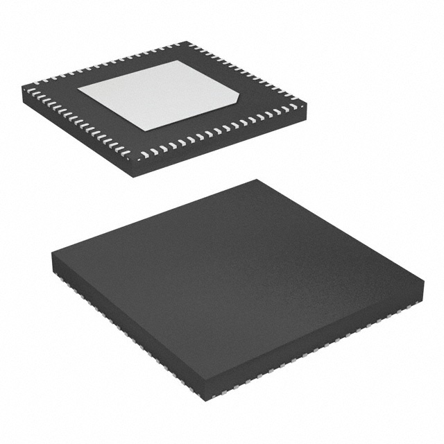
The AD9094 is available in a Pb-free, 72-lead, lead frame chip
scale package (LFCSP) and is specified over a junction
temperature range of −40°C to +105°C. This product may be
protected by one or more U.S. or international patents.
Note that throughout this data sheet, multifunction pins, such
as PDWN/STBY, are referred to either by the entire pin name
or by a single function of the pin, for example, PDWN, when
only that function is relevant.
PRODUCT HIGHLIGHTS
1.
2.
3.
4.
5.
6.
Rev. 0
Low power consumption per channel.
JESD204B lane rate support up to 15 Gbps.
Wide, full power bandwidth that supports IF sampling of
signals up to 1.4 GHz.
Buffered inputs that ease filter design and implementation.
Programmable, fast overrange detection.
On-chip temperature diode for system thermal management.
Document Feedback
Information furnished by Analog Devices is believed to be accurate and reliable. However, no
responsibility is assumed by Analog Devices for its use, nor for any infringements of patents or other
rights of third parties that may result from its use. Specifications subject to change without notice.
No license is granted by implication or otherwise under any patent or patent rights of Analog
Devices. Trademarks and registered trademarks are the property of their respective owners.
One Technology Way, P.O. Box 9106, Norwood, MA 02062-9106, U.S.A.
Tel: 781.329.4700
©2020 Analog Devices, Inc. All rights reserved.
Technical Support
www.analog.com
�AD9094
Data Sheet
TABLE OF CONTENTS
Features .............................................................................................. 1
Functional Overview ................................................................. 31
Applications ...................................................................................... 1
JESD204B Link Establishment ................................................. 31
General Description ......................................................................... 1
PHY (Driver) Outputs ............................................................... 32
Product Highlights ........................................................................... 1
JESD204B Transmitter Converter Mapping .......................... 33
Revision History ............................................................................... 2
Configuring the JESD204B Link .............................................. 34
Functional Block Diagram .............................................................. 3
Latency ............................................................................................. 36
Specifications .................................................................................... 4
End to End Total Latency ......................................................... 36
DC Specifications ......................................................................... 4
Example Latency Calculations ................................................. 36
AC Specifications ......................................................................... 5
LMFC Referenced Latency ....................................................... 36
Digital Specifications ................................................................... 6
Deterministic Latency.................................................................... 37
Switching Specifications .............................................................. 7
Subclass 0 Operation ................................................................. 37
Timing Specifications .................................................................. 8
Subclass 1 Operation ................................................................. 37
Absolute Maximum Ratings ......................................................... 10
Multichip Synchronization ........................................................... 39
Thermal Resistance .................................................................... 10
Normal Mode ............................................................................. 39
ESD Caution................................................................................ 10
Timestamp Mode ....................................................................... 39
Pin Configuration and Function Descriptions .......................... 11
SYSREF± Input........................................................................... 41
Typical Performance Characteristics ........................................... 13
SYSREF± Setup and Hold Window Monitor ........................ 42
Equivalent Circuits ......................................................................... 18
Test Modes ...................................................................................... 44
Theory of Operation ...................................................................... 20
ADC Test Modes ........................................................................ 44
ADC Architecture ...................................................................... 20
JESD204B Block Test Modes .................................................... 45
Analog Input Considerations ................................................... 20
SPI..................................................................................................... 47
Voltage Reference....................................................................... 21
Configuration Using the SPI .................................................... 47
DC Offset Calibration ................................................................ 22
Hardware Interface .................................................................... 47
Clock Input Considerations...................................................... 22
SPI Accessible Features ............................................................. 47
ADC Overrange and Fast Detect.................................................. 25
Memory Map .................................................................................. 48
ADC Overrange .......................................................................... 25
Reading the Memory Map Register Table .............................. 48
Fast Threshold Detection (FD_A, FD_B, FD_C, and FD_D)
....................................................................................................... 25
Memory Map Register ............................................................... 49
Applications Information ............................................................. 66
Signal Monitor ................................................................................ 26
Power Supply Recommendations ............................................ 66
SPORT Over JESD204B ............................................................ 26
Exposed Pad Thermal Heat Slug Recommendations ........... 66
Digital Outputs ............................................................................... 29
AVDD1_SR (Pin 64) and AGND_SR (Pin 63 and Pin 67) .. 66
Introduction to the JESD204B Interface ................................. 29
Outline Dimensions ....................................................................... 67
Setting Up the AD9094 Digital Interface ................................ 29
Ordering Guide .......................................................................... 67
REVISION HISTORY
10/2020—Revision 0: Initial Version
Rev. 0 | Page 2 of 67
�Data Sheet
AD9094
FUNCTIONAL BLOCK DIAGRAM
AVDD1
(0.9V)
VIN+A
AVDD1_SR
(0.9V)
BUFFER
VIN–A
AVDD2 AVDD3
(1.8V)
(2.5V)
DVDD
(0.9V)
FD_B
VIN+B
FAST
DETECT
JESD204B
HIGH SPEED
SERIALIZER
SIGNAL
MONITOR
BUFFER
SPIVDD
(1.8V)
2
TRANSMITTER
OUTPUTS
SERDOUTAB1±
SIGNAL
MONITOR
AND FAST
DETECT
CLK–
SYSREF±
JESD204B
SUBCLASS 1
CONTROL
CLOCK
GENERATION
CLK+
SERDOUTAB0±
8
ADC
CORE
VIN–B
DRVDD2
(1.8V)
8
ADC
CORE
VCM_AB
FD_A
DRVDD1
(0.9V)
SYNCINB±AB
SYNCINB±CD
÷2
÷4
÷8
BUFFER
VIN–C
VCM_CD/VREF
FD_C
FD_D
VIN+D
VIN–D
FAST
DETECT
8
ADC
CORE
JESD204B
HIGH SPEED
SERIALIZER
SIGNAL
MONITOR
BUFFER
ADC
CORE
2
TRANSMITTER
OUTPUTS
SERDOUTCD0±
SERDOUTCD1±
14
SPI CONTROL
PDWN/STBY
AD9094
AGND_SR AGND DRGND
SDIO SCLK CSB
Figure 1.
Rev. 0 | Page 3 of 67
20963-001
VIN+C
�AD9094
Data Sheet
SPECIFICATIONS
DC SPECIFICATIONS
AVDD1 = AVDD1_SR = DVDD = DRVDD1 = 0.9 V, AVDD2 = DRVDD2 = SPIVDD = 1.8 V, AVDD3 = 2.5 V, 1 GSPS, clock divider = 2,
1.44 V p-p full-scale differential input, 0.5 V internal reference, analog input amplitude (AIN) = −1.0 dBFS, and default SPI settings,
unless otherwise noted. Minimum and maximum specifications are guaranteed for the full operating TJ range of −40°C to +105°C.
Typical specifications represent performance at TJ = 50°C (TA = 25°C).
Table 1.
Parameter
RESOLUTION
ACCURACY
No Missing Codes
Offset Error
Offset Matching
Gain Error
Gain Matching
Differential Nonlinearity (DNL)
Integral Nonlinearity (INL)
TEMPERATURE DRIFT
Offset Error
Gain Error
INTERNAL VOLTAGE REFERENCE
INPUT REFERRED NOISE
ANALOG INPUTS
Differential Input Voltage Range (Programmable)
Common-Mode Voltage (VCM)
Differential Input Capacitance1
Differential Input Resistance
Analog Input Full Power Bandwidth
POWER SUPPLY
AVDD1
AVDD1_SR
AVDD2
AVDD3
DVDD
DRVDD1
DRVDD2
SPIVDD
AVDD1 Current, IAVDD1
AVDD1_SR Current, IAVDD1_SR
AVDD2 Current, IAVDD2
AVDD3 Current, IAVDD3
DVDD Current, IDVDD2
DRVDD1 Current, IDRVDD11
DRVDD2 Current, IDRVDD21
SPIVDD Current, ISPIVDD
Min
8
Typ
Max
Guaranteed
0
0
−5.6
−0.1
−0.3
1.0
±0.0
±0
+5.6
3.7
+0.1
+0.3
49.5
172.7
0.5
2.6
Rev. 0 | Page 4 of 67
Unit
Bits
% FSR
% FSR
% FSR
% FSR
LSB
LSB
ppm/°C
ppm/°C
V
LSB rms
1.44
1.44
1.43
1.75
200
1.4
2.16
V p-p
V
pF
Ω
GHz
0.877
0.877
1.71
2.44
0.877
0.877
1.71
1.71
0.9
0.9
1.8
2.5
0.9
0.9
1.8
1.8
420
25
440
60
110
85
30
0.65
0.923
0.923
1.89
2.56
0.923
0.923
1.89
1.89
575
60
520
71
196
205
38
0.80
V
V
V
V
V
V
V
V
mA
mA
mA
mA
mA
mA
mA
mA
�Data Sheet
AD9094
Parameter
POWER CONSUMPTION
Total Power Dissipation (Including Output Drivers)2
Power-Down Dissipation
Standby3
Min
Typ
Max
Unit
1.6
0.3
1.2
2.0
W
mW
W
1
All lanes are running. Power dissipation on DRVDD1 changes with the lane rate and number of lanes used.
Full bandwidth mode.
3
Standby mode is controlled by the SPI.
2
AC SPECIFICATIONS
AVDD1 = AVDD1_SR = DVDD = DRVDD1 = 0.9 V, AVDD2 = DRVDD2 = SPIVDD = 1.8 V, AVDD3 = 2.5 V, 1 GSPS, clock divider = 2,
1.44 V p-p full-scale differential input, 0.5 V internal reference, AIN = −1.0 dBFS, and default SPI settings, unless otherwise noted.
Minimum and maximum specifications are guaranteed for the TJ range of −40°C to +105°C. Typical specifications represent
performance at TJ = 50°C (TA = 25°C).
Table 2.
Analog Input Full Scale =
1.44 V p-p
Parameter1, 2
ANALOG INPUT FULL SCALE
NOISE DENSITY3
SIGNAL-TO-NOISE RATIO (SNR)4
fIN = 10 MHz
fIN = 155 MHz
fIN = 451 MHz
fIN = 611 MHz
fIN = 871 MHz
fIN = 1391 MHz
SIGNAL-TO-NOISE-ANDDISTORTION RATIO (SINAD)
fIN = 10 MHz
fIN = 155 MHz
fIN = 451 MHz
fIN = 611 MHz
fIN = 871 MHz
fIN = 1391 MHz
EFFECTIVE NUMBER OF BITS
(ENOB)
fIN = 10 MHz
fIN = 155 MHz
fIN = 451 MHz
fIN = 611 MHz
fIN = 871 MHz
fIN = 1391 MHz
SPURIOUS-FREE DYNAMIC RANGE
(SFDR)
fIN = 10 MHz
fIN = 155 MHz
fIN = 451 MHz
fIN = 611 MHz
fIN = 871 MHz
fIN = 1391 MHz
Min
Typ
1.44
−136.1
49.1
49.1
49.1
48.6
48.5
48.4
49.1
49.1
49.1
48.5
48.5
48.4
7.9
7.9
7.9
7.8
7.8
7.7
71
71
71
71
70
70
Max
Analog Input Full Scale =
1.80 V p-p
Min
47.4
46.2
7.4
60
Typ
1.80
−136.1
Max
Analog Input Full Scale =
2.16 V p-p
Min
Typ
2.16
−136.2
Max
Unit
V p-p
dBFS/Hz
49.2
49.2
49.2
48.7
48.5
48.5
49.2
49.2
49.2
48.6
48.5
48.4
dBFS
dBFS
dBFS
dBFS
dBFS
dBFS
49.2
49.2
49.2
48.7
48.4
48.4
49.2
49.2
49.2
48.5
48.3
48.2
dBFS
dBFS
dBFS
dBFS
dBFS
dBFS
7.9
7.9
7.9
7.8
7.7
7.7
7.9
7.9
7.9
7.8
7.7
7.7
Bits
Bits
Bits
Bits
Bits
Bits
72
72
72
66
65
67
71
70
71
63
63
65
dBFS
dBFS
dBFS
dBFS
dBFS
dBFS
Rev. 0 | Page 5 of 67
�AD9094
Data Sheet
Analog Input Full Scale =
1.44 V p-p
Parameter1, 2
WORST OTHER, EXCLUDING
SECOND AND THIRD
HARMONIC
fIN = 10 MHz
fIN = 155 MHz
fIN = 451 MHz
fIN = 611 MHz
fIN = 871 MHz
fIN = 1391 MHz
CROSSTALK5
FULL POWER BANDWIDTH6
Min
Typ
−70
−70
−71
−72
−73
−75
82
1.4
Max
Analog Input Full Scale =
1.80 V p-p
Min
Typ
−71
−72
−72
−74
−72
−72
82
1.4
Max
Analog Input Full Scale =
2.16 V p-p
Min
Typ
Max
−70
−70
−71
−72
−73
−75
82
1.4
−64
Unit
dBFS
dBFS
dBFS
dBFS
dBFS
dBFS
dB
GHz
1
See the AN-835 Application Note, Understanding High Speed ADC Testing and Evaluation, for definitions and for details on how these tests were completed.
fIN is the analog input frequency.
3
Noise density is measured at a low analog input frequency (fA) of 30 MHz.
4
See Table 9 for recommended settings for the buffer current setting.
5
Crosstalk is measured at 155 MHz with a −1.0 dBFS analog input on one channel and no input on the adjacent channel.
6
Full power bandwidth is measured with the circuit shown in Figure 44.
2
DIGITAL SPECIFICATIONS
AVDD1 = 0.9 V, AVDD1_SR = 0.9 V, AVDD2 = 1.8 V, AVDD3 = 2.5 V, DVDD = 0.9 V, DRVDD1 = 0.9 V, DRVDD2 = 1.8 V,
SPIVDD = 1.8 V, 1 GSPS, clock divider = 2, 1.44 V p-p full-scale differential input, 0.5 V internal reference, AIN = −1.0 dBFS, and default
SPI settings, unless otherwise noted. Minimum and maximum specifications are guaranteed for the TJ range of −40°C to +105°C. Typical
specifications represent performance at TJ = 50°C (TA = 25°C).
Table 3.
Parameter
CLOCK INPUTS (CLK±)
Logic Compliance
Differential Input Voltage
Input VCM
Differential Input Resistance
Input Capacitance
SYSTEM REFERENCE (SYSREF) INPUTS (SYSREF±)2
Logic Compliance
Differential Input Voltage
Input VCM
Differential Input Resistance
Input Capacitance (Single-Ended per Pin)
LOGIC INPUTS (PDWN/STBY)
Logic Compliance
Logic 1 Voltage
Logic 0 Voltage
Input Resistance
Min
600
400
0.6
18
Typ
Max
Unit
LVDS/LVPECL1
800
1600
0.69
32
0.9
mV p-p
V
kΩ
pF
LVDS/LVPECL1
800
1800
0.69
2.2
22
0.7
mV p-p
V
kΩ
pF
CMOS1
0.65 × SPIVDD
0
0.35 × SPIVDD
10
Rev. 0 | Page 6 of 67
V
V
MΩ
�Data Sheet
AD9094
Parameter
LOGIC INPUTS (SDIO, SCLK, AND CSB)
Logic Compliance
Logic 1 Voltage
Logic 0 Voltage
Input Resistance
LOGIC OUTPUT (SDIO)
Logic Compliance
Logic 1 Voltage (IOH = 800 μA)3
Logic 0 Voltage (IOL = 50 μA)3
SYNCIN INPUT (SYNCINB±AB AND SYNCINB±CD)
Logic Compliance
Differential Input Voltage
Input VCM
Input Resistance (Differential)
Input Capacitance (Single-Ended per Pin)
LOGIC OUTPUTS (FD_A, FD_B, FD_C, AND FD_D)
Logic Compliance
Logic 1 Voltage
Logic 0 Voltage
Input Resistance
DIGITAL OUTPUTS (SERDOUTABx± AND SERDOUTCDx±, x = 0 OR 1)
Logic Compliance
Differential Output Voltage
Short-Circuit Current (ID SHORT)
Differential Termination Impedance
Min
Typ
Max
Unit
0.35 × SPIVDD
V
V
kΩ
CMOS1
0.65 × SPIVDD
0
56
CMOS1
SPIVDD − 0.45 V
0
0.45
LVDS/LVPECL/CMOS1
800
1800
0.69
2.2
22
0.7
400
0.6
18
V
V
mV p-p
V
kΩ
pF
CMOS1
0.8 × SPIVDD
0
56
V
V
kΩ
CML1
455.8
15
100
mV p-p
mA
Ω
0.5
1
LVDS is low voltage differential signaling, LVPECL is low voltage positive/pseudo emitter coupled logic, CMOS is complementary metal-oxide semiconductor, and CML
is current mode logic.
2
DC-coupled input only.
3
IOH is the sinking current when the pin has a logic level = 0, and IOL is sourcing current when the pin has a logic level = 1.
SWITCHING SPECIFICATIONS
AVDD1 = 0.9 V, AVDD1_SR = 0.9 V, AVDD2 = 1.8 V, AVDD3 = 2.5 V, DVDD = 0.9 V, DRVDD1 = 0.9 V, DRVDD2 = 1.8 V,
SPIVDD = 1.8 V, 1 GSPS, clock divider = 2, 1.44 V p-p full-scale differential input, 0.5 V internal reference, AIN = −1.0 dBFS, and default
SPI settings, unless otherwise noted. Minimum and maximum specifications are guaranteed for the TJ range of −40°C to +105°C. Typical
specifications represent performance at TJ = 50°C (TA = 25°C).
Table 4.
Parameter
CLOCK
Clock Rate (at CLK± Pins)
Maximum Sample Rate1
Minimum Sample Rate2
Clock Pulse Width High
Clock Pulse Width Low
OUTPUT
Unit Interval (UI)3
Rise Time (tR) (20% to 80% into 100 Ω Load)
Fall Time (tF) (20% to 80% into 100 Ω Load)
Phase-Locked Look (PLL) Lock Time
Data Rate per Channel (Nonreturn to Zero (NRZ))4
Min
Typ
0.3
1000
240
125
125
66.67
1.6875
Rev. 0 | Page 7 of 67
100
31.25
31.37
5
10
Max
Unit
2.4
GHz
MSPS
MSPS
ps
ps
593
ps
ps
ps
ms
Gbps
15
�AD9094
Parameter
LATENCY5
Pipeline Latency
Fast Detect Latency
WAKE-UP TIME
From Standby
From Power-Down
APERTURE
Aperture Delay (tA)
Aperture Uncertainty (Jitter, tj)
Out of Range Recovery Time
Data Sheet
Min
Typ
Max
Unit
30
Sample clock cycles
Sample clock cycles
45
3
10
ms
ms
160
44
1
ps
fs rms
Sample clock cycles
1
The maximum sample rate is the clock rate after the divider.
The minimum sample rate operates at 240 MSPS with L = 2 or L = 1. Use SPI Register 0x011A to reduce the threshold of the clock detection circuit.
3
Baud rate = 1/UI. A subset of this range can be supported.
4
The default is L = 2 for each link. This number can be changed based on the sample rate and decimation ratio.
5
L = 2, M = 2, F = 2 for each link. See the Setting Up the AD9094 Digital Interface section for more information.
2
TIMING SPECIFICATIONS
Table 5.
Parameter
CLK+ to SYSREF+ TIMING REQUIREMENTS
tSU_SR
tH_SR
SPI TIMING REQUIREMENTS
tDS
tDH
tCLK
tS
tH
tHIGH
tLOW
tACCESS
tDIS_SDIO
Test Conditions/Comments
See Figure 3
Device clock to SYSREF+ setup time
Device clock to SYSREF+ hold time
See Figure 4
Setup time between the data and the rising edge of SCLK
Hold time between the data and the rising edge of SCLK
SCLK period
Setup time between CSB and SCLK
Hold time between CSB and SCLK
Minimum SCLK period required in a logic high state
Minimum SCLK period required in a logic low state
Maximum time delay between falling edge of SCLK and output
data valid for a read operation
Time required for the SDIO pin to switch from an output to an input
relative to the CSB rising edge (not shown in Figure 4)
Rev. 0 | Page 8 of 67
Min
Typ
Max
−44.8
64.4
ps
ps
6
ns
ns
ns
ns
ns
ns
ns
ns
4
2
40
2
2
10
10
10
Unit
10
ns
�Data Sheet
AD9094
Timing Diagrams
APERTURE
DELAY
ANALOG
INPUT
SIGNAL
N – 45
SAMPLE N
N – 44
N+1
N – 43
N – 42
N–1
N – 41
CLK–
20963-002
CLK+
Figure 2. Data Output Timing (Full Bandwidth Mode; L = 2, M = 2, F = 2), N = Sample Number
CLK–
CLK+
tSU_SR
tH_SR
20963-003
SYSREF–
SYSREF+
Figure 3. SYSREF± Setup and Hold Timing
tDS
tS
tHIGH
tCLK
tDH
tACCESS
tH
tLOW
CSB
SDIO DON’T CARE
DON’T CARE
R/W
A14
A13
A12
A11
A10
A9
A8
A7
D7
Figure 4. Serial Port Interface Timing Diagram
Rev. 0 | Page 9 of 67
D6
D3
D2
D1
D0
DON’T CARE
20963-004
SCLK DON’T CARE
�AD9094
Data Sheet
ABSOLUTE MAXIMUM RATINGS
THERMAL RESISTANCE
Table 6.
Parameter
Electrical
AVDD1 to AGND
AVDD1_SR to AGND
AVDD2 to AGND
AVDD3 to AGND
DVDD to DGND
DRVDD1 to DRGND
DRVDD2 to DRGND
SPIVDD to AGND
VIN±x to AGND
CLK± to AGND
SCLK, SDIO, CSB to DGND
PDWN/STBY to DGND
SYSREF± to AGND_SR
SYNCINB±AB/SYNCINB±CD to
DRGND
Environmental
Operating Junction Temperature
Range
Maximum Junction Temperature
Storage Temperature Range
(Ambient)
Rating
1.05 V
1.05 V
2.00 V
2.70 V
1.05 V
1.05 V
2.00 V
2.00 V
−0.3 V to AVDD3 + 0.3 V
−0.3 V to AVDD1 + 0.3 V
−0.3 V to SPIVDD + 0.3 V
−0.3 V to SPIVDD + 0.3 V
0 V to 2.5 V
0 V to 2.5 V
Thermal performance is directly linked to printed circuit board
(PCB) design and operating environment. Careful attention to
PCB thermal design is required.
θJA is the natural convection junction to ambient thermal
resistance measured in a one cubic foot sealed enclosure.
θJC_BOT is the bottom junction to case thermal resistance.
Table 7. Thermal Resistance
Package Type
CP-72-10
PCB Type
JEDEC
2s2p
Board
10-Layer
Board
1
Airflow
Velocity
(m/sec)
0.0
1.0
2.5
0.0
θJA
21.581, 2
17.941, 2
16.581, 2
9.74
θJC_BOT
1.951, 3
N/A4
N/A4
1.00
Per JEDEC 51-7, plus JEDEC 51-5 2s2p test board.
Per JEDEC JESD51-2 (still air) or JEDEC JESD51-6 (moving air).
3
Per MIL-STD 883, Method 1012.1.
4
N/A means not applicable.
2
−40°C to +105°C
ESD CAUTION
125°C
−65°C to +150°C
Stresses at or above those listed under Absolute Maximum
Ratings may cause permanent damage to the product. This is a
stress rating only; functional operation of the product at these
or any other conditions above those indicated in the operational
section of this specification is not implied. Operation beyond
the maximum operating conditions for extended periods may
affect product reliability.
Rev. 0 | Page 10 of 67
Unit
°C/W
°C/W
°C/W
°C/W
�Data Sheet
AD9094
72
71
70
69
68
67
66
65
64
63
62
61
60
59
58
57
56
55
AVDD2
AVDD1
AVDD1
AVDD1
AVDD1
AGND_SR
SYSREF–
SYSREF+
AVDD1_SR
AGND_SR
AVDD1
CLK–
CLK+
AVDD1
AVDD1
AVDD1
AVDD1
AVDD2
PIN CONFIGURATION AND FUNCTION DESCRIPTIONS
1
2
3
4
5
6
7
8
9
10
11
12
13
14
15
16
17
18
AD9094
TOP VIEW
(Not to Scale)
54
53
52
51
50
49
48
47
46
45
44
43
42
41
40
39
38
37
AVDD3
VIN–C
VIN+C
AVDD2
AVDD2
AVDD3
VIN+D
VIN–D
AVDD2
AVDD1
AVDD1
VCM_CD/VREF
DVDD
DGND
SPIVDD
CSB
SCLK
SDIO
NOTES
1. EXPOSED PAD. ANALOG GROUND. THE EXPOSED THERMAL PAD ON THE BOTTOM OF THE PACKAGE
PROVIDES THE GROUND REFERENCE FOR AVDDx, SPIVDD, DVDD, DRVDD1, AND DRVDD2.
THIS EXPOSED PAD MUST BE CONNECTED TO GROUND FOR PROPER OPERATION.
20963-005
SYNCINB–AB
SYNCINB+AB
DRGND
DRVDD1
SERDOUTAB0–
SERDOUTAB0+
SERDOUTAB1–
SERDOUTAB1+
SERDOUTCD1+
SERDOUTCD1–
SERDOUTCD0+
SERDOUTCD0–
DRVDD1
DRGND
SYNCINB+CD
SYNCINB–CD
FD_D
FD_C
19
20
21
22
23
24
25
26
27
28
29
30
31
32
33
34
35
36
AVDD3
VIN–A
VIN+A
AVDD2
AVDD2
AVDD3
VIN+B
VIN–B
AVDD2
AVDD1
AVDD1
VCM_AB
DVDD
DGND
DRVDD2
PDWN/STBY
FD_A
FD_B
Figure 5. Pin Configuration (Top View)
Table 8. Pin Function Descriptions
Pin No.
1, 6, 49, 54
2, 3
4, 5, 9, 46, 50, 51, 55, 72
7, 8
10, 11, 44, 45, 56 to 59, 62, 68 to 71
12
Mnemonic
AVDD3
VIN−A, VIN+A
AVDD2
VIN+B, VIN−B
AVDD1
VCM_AB
Type
Supply
Input
Supply
Input
Supply
Output
13, 42
14, 41
15
16
DVDD
DGND
DRVDD2
PDWN/STBY
Supply
Ground
Supply
Input
17, 18, 35, 36
Output
19
FD_A, FD_B,
FD_D, FD_C
SYNCINB−AB
20
SYNCINB+AB
Input
21, 32
22, 31
DRGND
DRVDD1
Ground
Supply
Input
Description
Analog Power Supply (2.5 V Nominal).
ADC A Analog Input Complement/True.
Analog Power Supply (1.8 V Nominal).
ADC B Analog Input True/Complement.
Analog Power Supply (0.9 V Nominal).
Common-Mode Level Bias Output for Analog Input Channel A and
Channel B.
Digital Power Supply (0.9 V Nominal).
Ground Reference for DVDD and SPIVDD.
Digital Power Supply for JESD204B PLL (1.8 V Nominal).
Power-Down Input/Standby (Active High). The operation of PDWN/STBY
depends on the mode that the device is placed in through the SPI and
can be configured as either power-down or standby. PDWN/STBY
requires an external 10 kΩ pull-down resistor.
Fast Detect Outputs for Channel A, Channel B, Channel C, and Channel D,
Respectively.
Active Low JESD204B LVDS Sync Input Complement for Channel A and
Channel B.
Active Low JESD204B LVDS/CMOS Sync Input True for Channel A and
Channel B.
Ground Reference for DRVDD1 and DRVDD2.
Digital Power Supply for SERDOUTABx± and SERDOUTCDx± (0.9 V
Nominal).
Rev. 0 | Page 11 of 67
�AD9094
Pin No.
23, 24
Data Sheet
Type
Output
Description
Lane 0 Output Data Complement/True for Channel A and Channel B.
Output
Lane 1 Output Data Complement/True for Channel A and Channel B.
Output
Lane 1 Output Data True/Complement for Channel C and Channel D.
Output
Lane 0 Output Data True/Complement for Channel C and Channel D.
33
Mnemonic
SERDOUTAB0−,
SERDOUTAB0+
SERDOUTAB1−,
SERDOUTAB1+
SERDOUTCD1+,
SERDOUTCD1−
SERDOUTCD0+,
SERDOUTCD0−
SYNCINB+CD
Input
34
SYNCINB−CD
Input
37
SDIO
38
39
40
43
SCLK
CSB
SPIVDD
VCM_CD/VREF
Input/
Output
Input
Input
Supply
Output/
Input
Active Low JESD204B LVDS/CMOS/LVPECL Sync Input True for Channel C
and Channel D.
Active Low JESD204B LVDS/CMOS/LVPECL Sync Input Complement for
Channel C and Channel D.
SPI Serial Data Input/Output.
47, 48
52, 53
60, 61
63, 67
64
65, 66
VIN−D, VIN+D
VIN+C, VIN−C
CLK+, CLK−
AGND_SR
AVDD1_SR
SYSREF+,
SYSREF−
AGND/EPAD
25, 26
27, 28
29, 30
Input
Input
Input
Ground
Supply
Input
SPI Serial Clock.
SPI Chip Select (Active Low).
Digital Power Supply for SPI (1.8 V Nominal).
Common-Mode Level Bias Output for Analog Input Channel C and
Channel D or 0.5 V Reference Voltage Input. VCM_CD/VREF is configurable
through the SPI as an output or an input. Use VCM_CD/VREF as the
common-mode level bias output when using the internal reference.
VCM_CD/VREF requires a 0.5 V reference voltage input when using an
external voltage reference source.
ADC D Analog Input Complement/True.
ADC C Analog Input True/Complement.
Clock Input True/Complement.
Ground Reference for SYSREF±.
Analog Power Supply for SYSREF± (0.9 V Nominal).
Active Low JESD204B LVDS System Reference Input True/Complement.
DC-coupled input only.
Exposed Pad. Analog ground. The exposed thermal pad on the bottom
of the package provides the ground reference for AVDDx, SPIVDD, DVDD,
DRVDD1, and DRVDD2. This exposed pad must be connected to ground
for proper operation.
Rev. 0 | Page 12 of 67
�Data Sheet
AD9094
TYPICAL PERFORMANCE CHARACTERISTICS
AVDD1 = AVDD1_SR = DVDD = DRVDD1 = 0.9 V, AVDD2 = DRVDD2 = SPIVDD = 1.8 V, AVDD3 = 2.5 V, 1 GSPS, clock divider = 2,
1.44 V p-p full-scale differential input, 0.5 V internal reference, AIN = −1.0 dBFS, and default SPI settings, unless otherwise noted.
Minimum and maximum specifications are guaranteed for the TJ range of −40°C to +105°C. Typical specifications represent
performance at TJ = 50°C (TA = 25°C).
0
0
–15
–15
–30
–30
–45
–45
–60
dB
–90
–90
–105
–105
–120
–120
–135
–135
50
100
150
200
250
300
350
400
450
FREQUENCY (MHz)
0
–30
–30
–45
–45
–60
–60
dB
0
–15
–90
–105
–105
–120
–120
–135
–135
100
150
200
250
300
350
400
450
FREQUENCY (MHz)
0
250
300
350
400
450
50
100
150
200
250
300
350
400
450
FREQUENCY (MHz)
Figure 10. Single-Tone FFT with fIN = 871 MHz, SNRFS = 48.5 dBFS,
SFDR = 70 dBFS, SINAD = 48.5 dBFS
Figure 7. Single-Tone FFT with fIN = 155 MHz, SNRFS = 49.1 dBFS,
SFDR = 71 dBFS, SINAD = 49.1 dBFS
0
0
–15
–30
–30
–45
–45
–60
–60
–75
–75
–90
–90
–105
–105
–120
–120
–135
–135
0
50
100
150
200
250
300
350
400
450
FREQUENCY (MHz)
Figure 8. Single-Tone FFT with fIN = 451 MHz, SNRFS = 49.1 dBFS,
SFDR = 71 dBFS, SINAD = 49.1 dBFS
0
50
100
150
200
250
300
FREQUENCY (MHz)
350
400
450
20963-011
dB
–15
20963-008
dB
200
–75
–90
20963-007
dB
0
50
150
Figure 9. Single-Tone FFT with fIN = 611 MHz, SNRFS = 48.6 dBFS,
SFDR = 71 dBFS, SINAD = 48.5 dBFS
–15
0
100
FREQUENCY (MHz)
Figure 6. Single-Tone Fast Fourier Transform (FFT) with fIN = 10 MHz, Signal to
Noise Ratio Full Scale (SNRFS) = 49.1 dBFS, SFDR = 71 dBFS, SINAD = 49.1 dBFS
–75
50
20963-010
0
20963-009
–75
20963-006
dB
–60
–75
Figure 11. Single-Tone FFT with fIN = 1391 MHz, SNRFS = 48.4 dBFS,
SFDR = 70 dBFS, SINAD = 48.4 dBFS
Rev. 0 | Page 13 of 67
�AD9094
Data Sheet
100
80
AVERAGE OF SNRFS
80
SNR/SFDR (dBFS)
SNR/SFDR (dBFS)
70
60
60
40
50
20
300
450
600
750
900
0
–100
20963-012
40
150
1050
fS (MSPS)
–80
–60
–40
–20
0
ANALOG INPUT AMPLITUDE (dBFS)
Figure 12. SNR/SFDR vs. Sample Rate (fS), fIN = 155 MHz
20963-015
SNR
SFDR
Figure 15. SNR/SFDR vs. Analog Input Amplitude, fIN = 155 MHz
100
80
70
80
SNR/SFDR (dBFS)
SNR/SFDR (dBFS)
60
50
40
30
60
40
20
20
0
100
200
300
400
500
600
700
fIN (MHz)
0
–100
20963-013
0
SNR
SFDR
SNR
SFDR
–80
–60
–40
–20
0
ANALOG INPUT AMPLITUDE (dBFS)
Figure 13. SNR/SFDR vs. fIN, AIN < 735MHz, Buffer Current = 160 μA
20963-016
10
Figure 16. SNR/SFDR vs. Analog Input Amplitude, fIN = 611 MHz
80
80
70
60
SNR/SFDR (dBFS)
50
40
30
20
0
700
20
SNR
SFDR
SNR
SFDR
800
900
1000
1100
fIN (MHz)
1200
1300
20963-014
10
40
0
–40
10
60
110
JUNCTION TEMPERATURE (°C)
Figure 17. SNR/SFDR vs. Junction Temperature, fIN = 155 MHz
Figure 14. SNR/SFDR vs. fIN, AIN ≥ 735 MHz, Buffer Current = 320 μA
Rev. 0 | Page 14 of 67
20963-017
SNR/SFDR (dBFS)
60
�Data Sheet
AD9094
80
25000
20000
NUMBER OF HITS
SNR/SFDR (dBFS)
60
40
15000
10000
20
5000
OUTPUT CODE
2.00
0
25
50
75
100
125
150
175
200
225
250
OUTPUT CODE
1.75
1.50
1.25
1.00
175
475
575
675
775
875
975
1075
1175
Figure 22. Total Power Dissipation vs. fS
49.2
49.0
SNR (dBFS)
48.8
48.6
48.4
48.2
0
25
50
75
100
125
150
175
OUTPUT CODE
Figure 20. DNL, fIN = 10.3 MHz
200
225
250
47.8
0.134
0.213
0.328
0.518
0.775
DIFFERENTIAL VOLTAGE (V)
1.249
1.929
20963-123
48.0
20963-020
DNL (LSB)
375
fS (MSPS)
Figure 19. INL, fIN = 10.3 MHz
0.10
0.09
0.08
0.07
0.06
0.05
0.04
0.03
0.02
0.01
0
–0.01
–0.02
–0.03
–0.04
–0.05
–0.06
–0.07
–0.08
–0.09
–0.10
275
20963-022
TOTAL POWER DISSIPATION (W)
0.10
0.09
0.08
0.07
0.06
0.05
0.04
0.03
0.02
0.01
0
–0.01
–0.02
–0.03
–0.04
–0.05
–0.06
–0.07
–0.08
–0.09
–0.10
Figure 21. Input Referred Noise Histogram
20963-019
INL (LSB)
Figure 18. SNR/SFDR vs. Junction Temperature, fIN = 611 MHz
20963-021
N + 10
N+8
N+6
N+4
N+2
N
N–2
0
N–4
110
N–6
60
JUNCTION TEMPERATURE (°C)
N – 10
10
20963-018
0
–40
N–8
SNR
SFDR
Figure 23. SNR vs. Differential Voltage (Clock Amplitude), fIN = 155.3 MHz
Rev. 0 | Page 15 of 67
�AD9094
Data Sheet
50.0
73
72
49.5
71
49.0
69
SNR (dBFS)
68
67
48.0
66
65
160µA
200µA
240µA
280µA
0
100
47.5
200
300
400
500
600
700
fIN (MHz)
47.0
700
20963-023
64
63
48.5
Figure 24. SFDR vs. fIN with Different Buffer Current Settings, AIN < 735 MHz
1V p-p
1.4V p-p
1.8V p-p
2.16V p-p
800
900
1000
1100
1200
1300
fIN (MHz)
20963-126
SFDR (dBFS)
70
Figure 27. SNR vs. fIN with Different Analog Input Full Scales, AIN ≥ 735 MHz,
Buffer Current = 320 μA
75
73
72
70
71
69
68
67
65
60
66
320µA
360µA
400µA
440µA
64
63
700
800
1V p-p
1.4V p-p
1.8V p-p
2.16V p-p
55
900
1000
1100
1200
1300
fIN (MHz)
50
20963-124
65
Figure 25. SFDR vs. fIN with Different Buffer Current Settings, AIN ≥ 735 MHz
0
100
200
300
400
500
600
700
fIN (MHz)
20963-127
SFDR (dBFS)
SFDR (dBFS)
70
Figure 28. SFDR vs. fIN with Different Analog Input Full Scales, AIN < 735 MHz
50.0
75
49.5
70
SFDR (dBFS)
SNR (dBFS)
49.0
48.5
65
60
48.0
0
100
200
300
400
fIN (MHz)
500
600
700
50
700
20963-125
47.0
55
Figure 26. SNR vs. fIN with Different Analog Input Full Scales, AIN < 735 MHz
1V p-p
1.4V p-p
1.8V p-p
2.16V p-p
800
900
1000
1100
fIN (MHz)
1200
1300
20963-128
1V p-p
1.4V p-p
1.8V p-p
2.16V p-p
47.5
Figure 29. SFDR vs. fIN with Different Analog Input Full Scales, AIN ≥ 735 MHz,
Buffer Current = 320 μA
Rev. 0 | Page 16 of 67
�Data Sheet
AD9094
0.10
2
0.09
–2
POWER (dB)
–4
0.08
0.07
–6
–8
–10
–12
–14
0.06
–16
–18
Figure 31. Full Power Bandwidth
Figure 30. AVDD3 Current vs. Buffer Current Setting
Rev. 0 | Page 17 of 67
1800
1595
1545
20963-200
fIN (MHz)
1495
1445
1495
1345
1295
1245
1195
1145
825
1075
–20
575
360
0
260
BUFFER CURRENT SETTING (µA)
325
0.05
160
20963-129
AVDD3 CURRENT (A)
0
�AD9094
Data Sheet
EQUIVALENT CIRCUITS
AVDD3
AVDD3
VIN+x
3.5pF
AVDD3
400Ω
VCM
BUFFER
EMPHASIS/SWING
CONTROL (SPI)
10pF
AVDD3
100Ω
DRVDD1
AVDD3
DATA+
SERDOUTABx+/SERDOUTCDx+
x = 0, 1
VIN–x
AIN
CONTROL
(SPI)
DRGND
OUTPUT
DRIVER
DRVDD1
DATA–
20963-024
3.5pF
SERDOUTABx–/SERDOUTCDx–
x = 0, 1
DRGND
Figure 32. Analog Inputs
20963-027
100Ω
Figure 35. Digital Outputs
DRVDD1
DRGND
2.5kΩ
CLK+
SYNCINB+AB/
SYNCINB+CD
25Ω
DRVDD1
100Ω
10kΩ
1.9pF
DRGND
130kΩ
LEVEL
TRANSLATOR
DRGND
16kΩ
130kΩ
DRVDD1
AVDD1
CLK–
100Ω
SYNCINB–AB/
SYNCINB–CD
25Ω
16kΩ
10kΩ
20963-025
1.9pF
VCM = 0.95V
DRGND
20963-028
AVDD1
CMOS
PATH
SYNCINB PIN
CONTROL (SPI)
DRGND
Figure 36. SYNCINB±AB, SYNCINB±CD Inputs
Figure 33. Clock Inputs
AVDD1_SR
100Ω
10kΩ
1.9pF
130kΩ
SPIVDD
LEVEL
TRANSLATOR
130kΩ
100Ω
SPIVDD
SCLK
10kΩ
56kΩ
1.9pF
20963-026
SYSREF–
ESD
PROTECTED
AVDD1_SR
Figure 34. SYSREF± Inputs
ESD
PROTECTED
DGND
Figure 37. SCLK Input
Rev. 0 | Page 18 of 67
DGND
20963-029
SYSREF+
�Data Sheet
AD9094
SPIVDD
ESD
PROTECTED
SPIVDD
ESD
PROTECTED
56kΩ
PDWN/
STBY
ESD
PROTECTED
ESD
PROTECTED
DGND
DGND
20963-030
DGND
DGND
Figure 38. CSB Input
Figure 41. PDWN/STBY Input
SPIVDD
SPIVDD
SDI
DGND
56kΩ
ESD
PROTECTED
SPIVDD
SDO
DGND
AGND
SPIVDD
SPIVDD
FD_A/FD_B/
FD_C/FD_D
FD
JESD204B LMFC
56kΩ
JESD204B SYNC
DGND
FD_x PIN CONTROL (SPI)
DGND
20963-032
DGND
VREF PIN
CONTROL (SPI)
Figure 42. VCM_CD/VREF Input/Output
Figure 39. SDIO Input
ESD
PROTECTED
TEMPERATURE
DIODE VOLTAGE
EXTERNAL REFERENCE
VOLTAGE INPUT
VCM_CD/VREF
DGND
DGND
AVDD2
20963-031
SDIO
Figure 40. FD_A, FD_B, FD_C, or FD_D Outputs
Rev. 0 | Page 19 of 67
20963-034
ESD
PROTECTED
ESD
PROTECTED
PDWN
CONTROL (SPI)
20963-033
CSB
�AD9094
Data Sheet
THEORY OF OPERATION
ADC ARCHITECTURE
Differential Input Configurations
The AD9094 architecture consists of an input buffered, pipelined
ADC. The input buffer of the ADC provides a 200 Ω termination
impedance to the analog input signal. The equivalent circuit
diagram of the analog input termination is shown in Figure 32.
There are several ways to drive the AD9094 actively or passively.
However, to achieve optimum performance, drive the analog
input differentially.
ANALOG INPUT CONSIDERATIONS
The analog input to the AD9094 is a differential buffer with an
internal VCM of 1.43 V. The clock signal alternately switches the
input circuit between sample mode and hold mode. Either a
differential capacitor or two single-ended capacitors can be
placed on the inputs to provide a matching passive network.
This configuration ultimately creates a low-pass filter at the input
that limits unwanted broadband noise. See Figure 43 and Figure 44
for details on input network recommendations.
For applications where SNR and SFDR are key parameters,
differential transformer coupling is the recommended input
configuration (see Figure 43 and Figure 44) because the noise
performance of most amplifiers is not adequate to achieve the
true performance of the AD9094.
For low to midrange frequencies, a double balun or double
transformer network is recommended for optimum performance
of the AD9094 (see Figure 43). For higher frequencies in the
third or fourth Nyquist zones, remove some of the front-end
passive components to ensure wideband operation (see Figure 44).
AGND
0.1µF
10Ω
2pF
0Ω
10Ω
VIN+x
10Ω
50Ω
0.1µF
BALUN
2pF
AGND
0.1µF
50Ω
10Ω
10Ω
0Ω
10Ω
VIN–x
For optimal dynamic performance, match the source impedances
driving VIN+x and VIN−x such that the common-mode settling
errors are symmetrical. These errors are reduced by the commonmode rejection of the ADC. An internal reference buffer creates
a differential reference that defines the span of the ADC core.
To achieve maximum SNR performance, set the ADC to the
largest span in a differential configuration. For the AD9094,
the available span is programmable through the SPI from
1.44 V p-p to 2.16 V p-p differential with 1.44 V p-p differential
as the default.
AGND
Figure 43. Differential Transformer Coupled Configuration AIN ≤ 735 MHz
AGND
0.1µF
10Ω
DNI
0Ω
50Ω
10Ω
VIN+x
DNI
0.1µF
BALUN
DNI
AGND
0.1µF
50Ω
10Ω
DNI
0Ω
10Ω
DNI
Dither
The AD9094 has internal on-chip dither circuitry that improves
the ADC linearity and SFDR, particularly at smaller signal levels. A
known but random amount of white noise is injected into the
AD9094 input. This dither improves the small signal linearity
within the ADC transfer function and is precisely subtracted out
digitally. The dither is turned on by default and does not reduce
the ADC input dynamic range. The specifications and limits in
this data sheet are obtained with the dither turned on. To disable
the dither, use the SPI writes to Register 0x0922. Disabling the
dither can slightly improve the SNR (by about 0.2 dB) at the
expense of the small signal SFDR.
20963-038
2pF
AGND
VIN–x
20963-039
The input buffer provides a linear, high input impedance (for
ease of drive) and reduces kickback from the ADC. The buffer
is optimized for high linearity, low noise, and low power. The
quantized outputs from each stage are combined into a final 8-bit
result in the digital correction logic. The pipelined architecture
allows the first stage to operate with a new input sample while
the remaining stages operate with the preceding samples at the
same time. Sampling occurs on the rising edge of the clock.
Figure 44. Differential Transformer Coupled Configuration for AIN > 735 MHz
Rev. 0 | Page 20 of 67
�Data Sheet
AD9094
0.10
Input Common Mode
The analog inputs of the AD9094 are internally biased to the
common mode, as shown in Figure 45.
AVDD3 CURRENT (A)
0.09
For dc-coupled applications, use the SPI writes listed in this section
to export the VCM to the VCM_CD/VREF pin. Use Register 0x1908
to disconnect the internal VCM buffer from the analog input.
When performing SPI writes for dc coupling operation, use the
following register settings in order:
4.
5.
6.
7.
8.
Analog Input Controls and SFDR Optimization
The AD9094 offers flexible controls for the analog inputs, such
as buffer current and input full-scale adjustment. All available
controls are shown in Figure 45.
AVDD3
0.05
160
260
360
BUFFER CURRENT SETTING (µA)
Figure 46. AVDD3 Power vs. Buffer Current Setting
In certain high frequency applications, the SFDR can be improved
by reducing the full-scale setting.
Table 9 shows the recommended buffer current settings for the
different analog input frequency (fA) ranges.
Table 9. SFDR Optimization for Input Frequencies
Analog Input
Frequencies
AIN < 500 MHz
AIN ≥ 500 MHz,
AIN < 735 MHz
AIN ≥ 735 MHz
Input Buffer Current Control Settings,
Register 0x1A4C and Register 0x1A4D
160 μA (Register 0x1A4C, Bits[5:0] =
Register 0x1A4D, Bits[5:0] = 01000)
280 μA (Register 0x1A4C, Bits[5:0] =
Register 0x1A4D, Bits[5:0] = 01110)
320 μA (Register 0x1A4C, Bits[5:0] =
Register 0x1A4D, Bits[5:0] = 10000)
Absolute Maximum Input Swing
The absolute maximum input swing allowed at the AD9094
inputs is 4.3 V p-p differential. Signals operating near or at
this level can cause permanent damage to the ADC.
AVDD3
VIN+x
3.5pF
VOLTAGE REFERENCE
AVDD3
100Ω
400Ω
A stable and accurate 0.5 V voltage reference is built into the
AD9094. This internal 0.5 V reference sets the full-scale input
range of the ADC. The full-scale input range can be adjusted via
Register 0x1910. For more information on adjusting the input
swing, see Table 23. Figure 47 shows the block diagram of the
internal 0.5 V reference controls.
VCM
BUFFER
10pF
AVDD3
100Ω
0.06
AVDD3
VIN–x
AIN
CONTROL
(SPI)
VIN+A/
VIN+B
20963-037
3.5pF
VIN–A/
VIN–B
INTERNAL
VREF
GENERATOR
Figure 45. Analog Input Controls
Use Register 0x1A4C and Register 0x1A4D to scale the buffer
currents on each channel to optimize the SFDR over various input
frequencies and bandwidths of interest. As the input buffer
currents are set, the amount of current required by the AVDD3
supply changes. This relationship is shown in Figure 46. For a
complete list of buffer current settings, see Table 23.
VREF
ADC
CORE
FULL-SCALE
VOLTAGE
ADJUST
INPUT FULL-SCALE
RANGE ADJUST
SPI REGISTER
(REGISTER 0x1910)
VREF PIN
CONTROL SPI
REGISTER
(REGISTER 0x18A6)
Figure 47. Internal Reference Configuration and Controls
Rev. 0 | Page 21 of 67
20963-040
2.
3.
Set Register 0x1908, Bit 2 to 1 to disconnect the internal
common-mode buffer from the analog input.
Set Register 0x18A6 to 0x00 to turn off the voltage reference.
Set Register 0x18E6 to 0x00 to turn off the temperature
diode export.
Set Register 0x18E0 to 0x04.
Set Register 0x18E1 to 0x1C.
Set Register 0x18E2 to 0x14.
Set Register 0x18E3, Bit 6 to 0x01 to turn on the VCM buffer to
export the internal common-mode voltage.
Set Register 0x18E3, Bits[5:0] to the buffer current setting
(copy the buffer current setting from Register 0x1A4C and
Register 0x1A4D to improve the accuracy of the commonmode export).
0.07
20963-146
1.
0.08
�AD9094
Data Sheet
INTERNAL
VREF
GENERATOR
FULL-SCALE
VOLTAGE
ADJUST
ADR130
NC
2
GND SET 5
3
VIN
0.1µF
NC 6
VOUT 4
VREF
0.1µF
VREF PIN AND
FULL-SCALE
VOLTAGE
CONTROL
20963-042
INPUT
1
Figure 48. External Reference Using the ADR130
Figure 49 shows a preferred method for clocking the AD9094. The
low jitter clock source is converted from a single-ended signal to a
differential signal using an RF transformer.
0.1µF
0.1µF
Figure 49. Transformer Coupled Differential Clock (Z is the Impedance Ratio)
Another option for clocking the AD9094 is to ac couple a
differential or LVDS signal to the sample clock input pins,
as shown in Figure 50.
0.1µF
The use of an external reference can be necessary in some
applications to enhance the gain accuracy of the ADC or to
improve thermal drift characteristics.
0.1µF
DC OFFSET CALIBRATION
The AD9094 contains a digital filter to remove the dc offset
from the output of the ADC. To enable this filter for ac-coupled
applications, set Register 0x0701, Bit 7 to 1 and set Register 0x073B,
Bit 7 to 0. The filter computes the average dc signal that is digitally
subtracted from the ADC output. As a result, the dc offset is
improved to better than 70 dBFS at the output. Because the filter
does not distinguish between the source of dc signals, this feature
can be used when the signal content at dc is not of interest. The
filter corrects dc up to ±512 codes and saturates beyond that.
CLOCK INPUT CONSIDERATIONS
For optimum performance, drive the AD9094 sample clock
inputs (CLK±) with a differential signal. This signal is typically
ac-coupled to the CLK± pins via a transformer or clock drivers.
These pins are biased internally and require no additional biasing.
0.1µF
CLK+
CLOCK INPUT
The external reference must be a stable 0.5 V reference. The
ADR130 is a sufficient option for providing the 0.5 V reference.
Figure 48 shows how the ADR130 provides the external 0.5 V
reference to the AD9094. The dashed lines show unused blocks
within the AD9094 while using the ADR130 to provide the
external reference.
ADC
CLK–
LVDS
DRIVER
CLK+
100Ω
CLK–
CLOCK INPUT
50Ω1
50Ω1
ADC
CLK–
0.1µF
1 50Ω RESISTORS ARE OPTIONAL.
20963-045
3.
Set Register 0x18E3 to 0x00 to turn off VCM export.
Set Register 0x18E6 to 0x00 to turn off temperature diode
export.
Set Register 0x18A6 to 0x01 to turn on the external voltage
reference.
CLK+
100Ω
50Ω
The SPI writes required to use the external voltage reference, in
order, are as follows:
1.
2.
1:1Z
CLOCK
INPUT
20963-043
Use Register 0x18A6 to either use the internal 0.5 V reference or
to provide an external 0.5 V reference. When using an external
voltage reference, always provide a 0.5 V reference. The full-scale
adjustment is made using the SPI and is irrespective of the
reference voltage. For more information on adjusting the fullscale level of the AD9094, refer to Table 23.
Figure 50. Differential LVDS Sample Clock
Clock Duty Cycle Considerations
Typical high speed ADCs use both clock edges to generate a variety
of internal timing signals. The AD9094 contains an internal clock
divider and a duty cycle stabilizer (DCS). In applications where
the clock duty cycle cannot be guaranteed to be 50%, a higher
multiple frequency clock with the usage of the clock divider is
recommended. When providing a higher frequency clock is not
possible, users are recommended to turn on the DCS. The divider
output offers a 50% duty cycle, high slew rate (fast edge) clock
signal to the internal ADC. The following SPI writes are
required to turn on DCS (see the Memory Map section for
more details on using this feature):
1.
2.
3.
4.
5.
Rev. 0 | Page 22 of 67
Write 0x81 to Register 0x011F.
Write 0x09 to Register 0x011C.
Write 0x09 to Register 0x011E.
Write 0x0B to Register 0x011C.
Write 0x0B to Register 0x011E.
�Data Sheet
AD9094
Input Clock Divider
The AD9094 contains an input clock divider with the ability
to divide the input clock by 1, 2, 4, or 8. To select the divider
ratios, use Register 0x0108 (see Figure 51).
In applications where the clock input is a multiple of the sample
clock, take care to program the appropriate divider ratio into the
clock divider before applying the clock signal to ensure that the
current transients during device startup are controlled.
CLK+
÷2
Figure 53 shows the estimated SNR of the AD9094 across fA for
different clock induced jitter values. To estimate the SNR, use
the following equation:
÷4
REGISTER 0x0108
20963-046
÷8
SNRJITTER
SNRADC
10
10 10
SNR(dBFS) 10log 10
Figure 51. Clock Divider Circuit
The AD9094 clock divider can be synchronized using the external
SYSREF± input. A valid SYSREF± causes the clock divider to
reset to a programmable state. This synchronization feature allows
multiple devices to have the corresponding clock dividers aligned
to guarantee simultaneous input sampling.
50
SNR (dBFS)
49
Clock Jitter Considerations
High speed, high resolution ADCs are sensitive to the quality of
the clock input. Calculate the degradation in SNR at a given fA
only in relation to tJ with the following equation:
47
46
SNR = −20 × log (2 × π × fA × tJ)
In this equation, the rms tJ represents the root mean square of
all jitter sources including the clock input, analog input signal,
and ADC tJ specifications. IF undersampling applications are
particularly sensitive to jitter (see Figure 52).
130
25f S
50f S
75f S
100fS
45
10M
125f S
150f S
175f S
200f S
100M
1G
INPUT FREQUENCY (Hz)
10G
Figure 53. Estimated SNR Degradation vs. Analog Input Frequency over RMS Jitter
Input Clock Detect
12.5fS
25fS
50fS
100fS
200fS
400fS
800fS
70
The AD9094 contains input clock detection circuitry to detect
the signal on the CLK± input clock pins. If the clock amplitude
or fS is lower than the specified minimum value, the AD9094
enters power-down mode. When the input clock detect bit in
Register 0x011B is set to 0, the input clock is not detected. See
Register 0x011A and Register 0x011B in Table 23 for more
details on the input clock detect feature.
60
Power-Down and Standby Mode
50
The AD9094 PDWN/STBY pin configures the device when in
power-down or standby mode. The default operation is powerdown. The PDWN/STBY pin is a logic high pin. When in powerdown mode, the JESD204B link is disrupted. The power-down
option can also be set via Register 0x003F and Register 0x0040.
120
110
100
90
80
40
30
10
100
1000
fIN (MHz)
Figure 52. Ideal SNR vs. fIN over Jitter
10000
20963-047
IDEAL SNR (dB)
48
20963-153
CLK–
Treat the clock input as an analog signal in cases where tJ can
affect the dynamic range of the AD9094. Separate the power
supplies for clock drivers from the ADC output driver supplies
to avoid modulating the clock signal with digital noise. If the clock
is generated from another type of source (by gating, dividing,
or other methods), retime the clock by using the original clock at
the last step. Refer to the AN-501 Application Note, Aperture
Uncertainty and ADC System Performance and the AN-756
Application Note, Sampled Systems and the Effects of Clock
Phase Noise and Jitter for more in depth information about
jitter performance as it relates to ADCs.
In standby mode, the JESD204B link is not disrupted and transmits
zeros for all converter samples. To change this state, use
Register 0x0571, Bit 7 to select /K/ characters.
Rev. 0 | Page 23 of 67
�AD9094
Data Sheet
5.
To enable the 20× diode , set Register 0x18E6 to 0x02 to
turn on the second central temperature diode of the pair,
which is 20× the size of the first. When using two diodes
simultaneously to achieve a more accurate result, see the
AN-1432 Application Note, Practical Thermal Modeling and
Measurements in High Power ICs for more information.
The AD9094 contains a diode-based temperature sensor to
measure the temperature of the die. This diode can output a
voltage and serve as a coarse temperature sensor to monitor
the internal die temperature.
The SPI writes required to export the temperature diode are as
follows (see Table 23 for more information):
1.
2.
3.
4.
0.80
TEMPERATURE DIODE VOLTAGE (V)
To output the temperature diode voltage to the VCM_CD/
VREF pin, use the SPI. Use Register 0x18E6 to enable or disable
the diode. Register 0x18E6 is a local register. Both cores must be
selected in the pair index register (Register 0x0009 = 0x03) to
enable the temperature diode readout. Note that other voltages
may be exported to the same pin at the same time, which can
result in undefined behavior. Therefore, to ensure a proper
readout, switch off all other voltage exporting circuits as detailed
in the following steps.
Set Register 0x0009 to 0x03 to select both cores.
Set Register 0x18E3 to 0x00 to turn off VCM export.
Set Register 0x18A6 to 0x00 to turn off voltage reference
export.
Set Register 0x18E6 to 0x01 to turn on the voltage export
of the central 1× temperature diode. The typical voltage
response of the temperature diode is shown in Figure 54.
Although this voltage represents the die temperature, take
measurements from a pair of diodes for improved accuracy.
Rev. 0 | Page 24 of 67
0.75
0.70
0.65
0.60
0.55
0.50
–40
–20
40
60
0
20
JUNCTION TEMPERATURE (°C)
80
100
Figure 54. Temperature Diode Voltage vs. Junction Temperature
20963-048
Temperature Diode
�Data Sheet
AD9094
ADC OVERRANGE AND FAST DETECT
The fast detect indicator is asserted if the input magnitude
exceeds the value programmed in the fast detect upper threshold
registers located at Register 0x0247 and Register 0x0248. The
selected threshold register is compared with the signal magnitude
at the ADC output. The fast upper threshold detection has a
latency of 30 clock cycles (maximum). The approximate upper
threshold magnitude (in dBFS) is defined by the following
equation:
In receiver applications, a mechanism to reliably determine when
the converter is about to be clipped is beneficial. The standard
overrange bit in the JESD204B outputs provides information
on the state of the analog input that is of limited usefulness.
Therefore, a programmable threshold below full scale that allows
time to reduce the gain before the clip actually occurs is helpful.
In addition, because input signals can have significant slew rates,
the latency of this function is of major concern. Highly pipelined
converters can have significant latency. The AD9094 contains fast
detect circuitry for individual channels to monitor the threshold
and to assert the FD_A, FD_B, FD_C, and FD_D pins.
Upper Threshold Magnitude = 20log (Threshold
Magnitude/213)
The fast detect indicators do not clear until the signal drops
below the lower threshold for the programmed dwell time. The
lower threshold is programmed in the fast detect lower threshold
registers located at Register 0x0249 and Register 0x024A. The
fast detect lower threshold register is a 13-bit register that is
compared with the signal magnitude at the ADC output. This
comparison is subject to the ADC pipeline latency, however,
the comparison is accurate in terms of converter resolution. The
lower threshold magnitude (in dBFS) is defined by the following
equation:
ADC OVERRANGE
The ADC overrange indicator is asserted when an overrange
is detected on the ADC input. The overrange indicator can be
embedded within the JESD204B link as a control bit (when
CSB > 0). The latency of this overrange indicator matches the
sample latency.
FAST THRESHOLD DETECTION (FD_A, FD_B, FD_C,
AND FD_D)
The fast detect FD_x bits in Register 0x0040 immediately
set whenever the absolute value of the input signal exceeds the
programmable upper threshold level. The FD_x bits clear only
when the absolute value of the input signal drops below the
lower threshold level for greater than the programmable dwell
time. This feature provides hysteresis and prevents the FD_x bits
from excessively toggling.
Lower Threshold Magnitude = 20log (Threshold Magnitude/213)
For example, to set an upper threshold of −6 dBFS, write 0xFFF
to Register 0x0247 and Register 0x0248. To set a lower threshold of
−10 dBFS, write 0xA1D to Register 0x0249 and Register 0x024A.
The dwell time can be programmed from 1 to 65,535 sample
clock cycles. To program the dwell time, pace the desired value
in the fast detect dwell time registers located at Register 0x024B
and Register 0x024C (see Table 23 for more details).
The operation of the upper threshold and lower threshold
registers with the dwell time registers is shown in Figure 55.
UPPER THRESHOLD
DWELL TIME
LOWER THRESHOLD
DWELL TIME
FD_x
Figure 55. Threshold Settings for the FD_x Signals
Rev. 0 | Page 25 of 67
TIMER COMPLETES BEFORE
SIGNAL RISES ABOVE
LOWER THRESHOLD
20963-050
MIDSCALE
TIMER RESET BY
RISE ABOVE
LOWER
THRESHOLD
�AD9094
Data Sheet
SIGNAL MONITOR
The signal monitor block provides additional information
on the signal being digitized by the ADC. The signal monitor
computes the peak magnitude of the digitized signal. This
information can drive an automatic gain control (AGC) loop
to optimize the range of the ADC in the presence of real-world
signals.
The results of the signal monitor block can be obtained either
by reading back the internal values from the SPI port or by
embedding the signal monitoring information into the
JESD204B interface as special control bits. A global, 24-bit
programmable period controls the duration of the measurement.
Figure 56 shows the simplified block diagram of the signal
monitor block.
SIGNAL MONITOR
PERIOD REGISTERS
(SMPR)
REGISTER 0x0271,
REGISTER 0x0272,
REGISTER 0x0273
CLEAR
FROM
INPUT
MAGNITUDE
STORAGE
REGISTER
LOAD
DOWN
COUNTER
When the monitor period timer reaches a count of 1, the 13-bit
peak level value is transferred to the signal monitor holding
register, which can be read through the memory map or output
through the SPORT interface over the JESD204B interface. The
monitor period timer is reloaded with the value in the SMPR
and the countdown restarts. The magnitude of the first input
sample is also updated in the magnitude storage register, and
the comparison and update procedure, as described in the Fast
Threshold Detection (FD_A, FD_B, FD_C, and FD_D) section,
continues.
IS
COUNT = 1?
LOAD
LOAD
SIGNAL
MONITOR
HOLDING
REGISTER
TO SPORT OVER
JESD204B AND
MEMORY MAP
SPORT OVER JESD204B
20963-051
FROM
MEMORY
MAP
COMPARE
A>B
When peak detection mode is enabled, the value in the SMPR
is loaded into a monitor period timer that decrements at the
decimated clock rate. The magnitude of the input signal is
compared with the value in the internal magnitude storage register
(not accessible to the user) and the greater of the two is updated
as the current peak level. The initial value of the magnitude
storage register is set to the current ADC input signal magnitude.
This comparison continues until the monitor period timer reaches
a count of 1.
Figure 56. Signal Monitor Block
The peak detector captures the largest signal within the
observation period. The detector only observes the magnitude
of the signal. The resolution of the peak detector is a 13-bit
value, and the observation period is 24 bits and represents
converter output samples. To derive the peak magnitude
(in dBFS), use the following equation:
Peak Magnitude = 20log(Peak Detector Value/213)
The magnitude of the input port signal is monitored over a
programmable time period that is determined by the signal
monitor period register (SMPR). To enable the peak detector
function, set Bit 1 of Register 0x0270 in the signal monitor control
register. The 24-bit SMPR must be programmed before activating
this mode.
The signal monitor data can also be serialized and sent over the
JESD204B interface as control bits. These control bits must be
deserialized from the samples to reconstruct the statistical data.
To enable the signal control monitor function, set Bit 0 of
Register 0x0279 and Bit 1 of Register 0x027A. Figure 57 shows
two different example configurations for the signal monitor
control bit locations inside the JESD204B samples. A maximum
of three control bits can be inserted into the JESD204B samples.
However, only one control bit is required for the signal monitor.
Control bits are inserted from MSB to LSB. If only one control bit
is to be inserted (number of control bits per sample (CS) = 1),
only the most significant control bit is used (see the Example
Configuration 1 and the Example Configuration 2 in Figure 57).
To select the SPORT over JESD204B (signal monitor) option,
program Register 0x0559, and Register 0x058F accordingly. See
Table 23 for more information on setting these bits.
Figure 58 shows the 25-bit frame data that encapsulates the
peak detector value. The frame data is transmitted MSB first
with five 5-bit subframes. Each subframe contains a start bit
that can be used by a receiver to validate the deserialized data.
Figure 59 shows the SPORT over JESD204B signal monitor
data with a monitor period timer set to 80 samples.
Rev. 0 | Page 26 of 67
�Data Sheet
AD9094
16-BIT JESD204B SAMPLE SIZE (N' = 16)
1-BIT
CONTROL
BIT
(CS = 1)
15-BIT CONVERTER RESOLUTION (N = 15)
EXAMPLE
CONFIGURATION 1
(N' = 16, N = 15, CS = 1)
15
S14
X
14
S13
X
13
S12
X
12
S11
X
11
10
S10
X
9
S9
X
8
S8
X
7
S7
X
6
S6
X
5
S5
X
S4
X
4
S3
X
3
S2
X
2
S1
X
1
0
S0
X
CTRL
BIT 2
X
SERIALIZED SIGNAL MONITOR
FRAME DATA
16-BIT JESD204B SAMPLE SIZE (N' = 16)
15
S13
X
14
S12
X
13
S11
X
12
S10
X
11
10
S9
X
9
S8
X
8
S7
X
7
S6
X
6
S5
X
5
S4
X
S3
X
4
S2
X
3
S1
X
2
1
0
S0
X
CTRL
BIT 2
X
TAIL
X
SERIALIZED SIGNAL MONITOR
FRAME DATA
Figure 57. Signal Monitor Control Bit Locations
5-BIT SUBFRAMES
5-BIT IDLE
SUBFRAME
(OPTIONAL)
IDLE
1
5-BIT IDENTIFIER START
0
SUBFRAME
25-BIT
FRAME
IDLE
1
IDLE
1
IDLE
1
IDLE
1
ID3
0
ID2
0
ID1
0
ID0
1
5-BIT DATA
MSB
SUBFRAME
START
0
P12
P11
P10
P9
5-BIT DATA
SUBFRAME
START
0
P8
P7
P6
P5
5-BIT DATA
SUBFRAME
START
0
P4
P3
P2
P1
5-BIT DATA
LSB
SUBFRAME
START
0
Px
0
0
0
Px TO P12 = PEAK MAGNITUDE VALUE
Figure 58. SPORT over JESD204B Signal Monitor Frame Data
Rev. 0 | Page 27 of 67
20963-052
14-BIT CONVERTER RESOLUTION (N = 14)
20963-053
EXAMPLE
CONFIGURATION 2
(N' = 16, N = 14, CS = 1)
1
CONTROL
1 TAIL
BIT
BIT
(CS = 1)
�AD9094
Data Sheet
SMPR = 80 SAMPLES (REGISTER 0x0271 = 0x50; REGISTER 0x0272 = 0x00; REGISTER 0x0273 = 0x00)
80-SAMPLE PERIOD
PAYLOAD 3
25-BIT FRAME (N)
IDENTIFIER
DATA
MSB
DATA
DATA
DATA
LSB
IDLE
IDLE
IDLE
IDLE
IDLE
IDLE
IDLE
IDLE
IDLE
IDLE
IDLE
IDLE
IDLE
IDLE
IDLE
IDLE
IDLE
IDLE
IDLE
IDLE
IDLE
IDLE
IDLE
IDLE
IDLE
80-SAMPLE PERIOD
PAYLOAD 3
25-BIT FRAME (N + 1)
IDENTIFIER
DATA
MSB
DATA
DATA
DATA
LSB
IDLE
IDLE
IDLE
IDLE
80-SAMPLE PERIOD
IDENTIFIER
DATA
MSB
DATA
DATA
DATA
LSB
IDLE
IDLE
IDLE
IDLE
Figure 59. SPORT over JESD204B Signal Monitor Data Example with Period Timer = 80 Samples
Rev. 0 | Page 28 of 67
20963-054
PAYLOAD 3
25-BIT FRAME (N + 2)
�Data Sheet
AD9094
DIGITAL OUTPUTS
INTRODUCTION TO THE JESD204B INTERFACE
The AD9094 digital outputs are designed to the JEDEC standard,
JESD204B, serial interface for data converters. JESD204B is a
protocol to link the AD9094 to a digital processing device over
a serial interface with lane rates up to 15 Gbps. The benefits of
the JESD204B interface over LVDS include a reduction in
required board area for data interface routing and an ability to
enable smaller packages for converter and logic devices.
SETTING UP THE AD9094 DIGITAL INTERFACE
The following SPI writes are required for the AD9094 at startup
and each time the ADC is reset (datapath reset, soft reset, link
power-down or power-up, or hard reset):
1.
2.
3.
4.
5.
6.
Write 0x4F to Register 0x1228.
Write 0x0F to Register 0x1228.
Write 0x04 to Register 0x1222.
Write 0x00 to Register 0x1222.
Write 0x08 to Register 0x1262.
Write 0x00 to Register 0x1262.
The JESD204B data transmit blocks in the AD9094 map up to
two physical ADCs over each of the two JESD204B links. Each
link can be configured to use one or two JESD204B lanes for
up to a total of four lanes for the AD9094 chip. The JESD204B
specification refers to a number of parameters to define the
link. These parameters must match between the JESD204B
transmitter (the AD9094 output) and the JESD204B receiver
(the logic device input). The JESD204B outputs of the AD9094
function effectively as two individual JESD204B links. The two
JESD204B links can be synchronized, if desired, using the
SYSREF± input.
Each JESD204B link is described according to the following
parameters:
The JESD204B data transmit block, JTX, assembles the parallel
data from the ADC into frames and uses 8-bit or 10-bit encoding
as well as optional scrambling to form serial output data. Lane
synchronization is supported through the use of special control
characters during the initial link establishment. Additional
control characters are embedded in the data stream to maintain
synchronization thereafter. A JESD204B receiver is required to
complete the serial link. For additional details on the JESD204B
interface, refer to the JESD204B standard.
L is the number of lanes per converter device (lanes per
link) (AD9094 value = 1 or 2).
M is the number of converters per converter device
(virtual converters per link) (AD9094 value = 1 or 2).
F is the number of octets per frame (AD9094 value = 1, 2,
4, or 8).
N΄ is the number of bits per sample (JESD204B word size)
(AD9094 value = 8).
N is the converter resolution (AD9094 value = 7 to 8).
CS is the number of control bits per sample (AD9094 value =
0 or 1).
K is the number of frames per multiframe (AD9094 value = 4,
8, 12, 16, 20, 24, 28, or 32 ).
S is the samples transmitted per single converter per frame
cycle (AD9094 value is set automatically based on L, M, F,
and N΄).
HD is high density mode (AD9094 value is set automatically
based on L, M, F, and N΄).
CF is the number of control words per frame clock cycle per
converter device (AD9094 value = 0).
Figure 60 shows a simplified block diagram of the AD9094
JESD204B transmit link. By default, the AD9094 is configured
to use four converters and four lanes. The Converter A and
Converter B data is output to the SERDOUTAB0± and
SERDOUTAB1± pins, and the Converter C and Converter D
data is output to the SERDOUTCD0± and SERDOUTCD1± pins.
The AD9094 allows other configurations, such as combining the
outputs of each pair of converters into a single lane or changing
the mapping of the digital output paths. These modes are set up
via a quick configuration register in the SPI register map, which
includes additional customizable options.
By default in the AD9094, the 8-bit converter word from each
converter is placed into an octet (eight bits of data).
By default, no tail bit is enabled. If enabled, the tail bits can be
configured as zeros or a pseudorandom number sequence. The
tail bits can also be replaced with control bits that indicate
overrange, SYSREF±, or fast detect output.
The resulting octet can be scrambled. Scrambling is optional,
however, avoiding spectral peaks when transmitting similar
digital data patterns is recommended. The scrambler uses a
self synchronizing, polynomial-based algorithm defined by
the equation 1 + x14 + x15. The descrambler in the receiver is a
self synchronizing version of the scrambler polynomial.
After the octet is scrambled The octet is then encoded with an
8-bit or 10-bit encoder. The 8-bit or 10-bit encoder takes eight bits
of data (an octet) and encodes the bits into a 10-bit symbol.
Figure 61 shows how the 8-bit data is taken from the ADC, the
tail bits are added (if enabled), the octet is scrambled, and the
octet is encoded into a 10-bit symbol. Figure 61 shows the
default data format.
Rev. 0 | Page 29 of 67
�AD9094
Data Sheet
CONVERTER A
INPUT
CONVERTER B
INPUT
ADC A
MUX/
FORMAT
(SPI REGISTERS:
0x0561, 0x0564)
JESD204B PAIR
A/B LINK
CONTROL
(L, M, F)
(SPI REGISTER
0x0570)
LANE MUX
AND MAPPING
(SPI
REGISTERS:
0x05B0,
0x05B2,
0x05B3)
MUX/
FORMAT
(SPI REGISTERS:
0x0561, 0x0564)
JESD204B PAIR
A/B LINK
CONTROL
(L, M, F)
(SPI REGISTER
0x0570)
LANE MUX
AND MAPPING
(SPI
REGISTERS:
0x05B0,
0x05B2,
0x05B3)
SERDOUTAB0+
SERDOUTAB0–
SERDOUTAB1+
SERDOUTAB1–
ADC B
SYSREF±
SYNCIN±AB
SYNCIN±CD
CONVERTER C
INPUT
CONVERTER D
INPUT
SERDOUTCD0+
SERDOUTCD0–
SERDOUTCD1+
SERDOUTCD1–
20963-064
ADC C
ADC D
Figure 60. Transmit Link Simplified Block Diagram with Full Bandwidth Mode
TAIL BITS
REGISTER 0x0571, BIT 6
LSB
A7
A6
A5
A4
A3
A2
A1
A0
A7
A6
A5
A4
A3
A2
A1
A0
MSB
LSB
SERIALIZER
8-BIT/10-BIT
ENCODER
S7
S6
S5
S4
S3
S2
S1
S0
OCTET 1
OCTET 0
OCTET 1
MSB
SAMPLE 0
SAMPLE 1
LSB
JESD204B SAMPLE
CONSTRUCTION
A7
A6
A5
A4
A3
A2
A1
A0
SCRAMBLER
1 + x14 + x15
(OPTIONAL)
S7
S6
S5
S4
S3
S2
S1
S0
a b ....
i
SYMBOL 0
a b c d e f g h i
j
a b c d e f g h i
j
SERDOUT0±
SERDOUT1±
j a b ....
i
j
SYMBOL 1
20963-065
ADC
A7
A6
A5
A4
A3
A2
A1
A0
FRAME
CONSTRUCTION
OCTET 0
ADC TEST PATTERNS
(REGISTER 0x0550,
REGISTER 0x0551 TO REGISTER 0x0558)
MSB
JESD204B DATA
LINK LAYER TEST
PATTERNS
REGISTER 0x0574, BITS[2:0]
JESD204B
INTERFACE TEST
PATTERNS
(REGISTER 0x0573,
REGISTER 0x0551 TO REGISTER 0x0558)
JESD204B LONG
TRANSPORT TEST
PATTERN
REGISTER 0x0571, BIT 5
Figure 61. ADC Output Datapath with Data Framing
PROCESSED
SAMPLES
FROM ADC
SAMPLE
CONSTRUCTION
FRAME
CONSTRUCTION
DATA LINK
LAYER
SCRAMBLER
ALIGNMENT
CHARACTER
GENERATION
8-BIT/10-BIT
ENCODER
PHYSICAL
LAYER
CROSSBAR
MUX
SERIALIZER
Tx
OUTPUT
20963-066
TRANSPORT
LAYER
SYSREF±
SYNCINB±xx
Figure 62. Data Flow
Rev. 0 | Page 30 of 67
�Data Sheet
AD9094
FUNCTIONAL OVERVIEW
The block diagram in Figure 62 shows the flow of data through
each of the two JESD204B links from the sample input to the
physical output. The processing can be divided into layers that
are derived from the open source initiative (OSI) model widely
used to describe the abstraction layers of communications
systems. These layers are the transport layer, data link layer,
and physical layer (PHY) (serializer and output driver).
Transport Layer
The transport layer packs the data, which consists of samples
and optional control bits, into JESD204B frames that are mapped
to 8-bit octets. These octets are sent to the data link layer. The
transport layer mapping is controlled by rules derived from the
link parameters. Tail bits are added to fill gaps where required.
Use the following equation to determine the number of tail bits
(T) within a sample (JESD204B word):
T = N΄ − N − CS
Data Link Layer
The data link layer is responsible for the low level functions of
passing data across the link. These functions include optionally
scrambling the data, inserting control characters for multichip
synchronization, lane alignment, or monitoring, as well as
encoding 8-bit octets into 10-bit symbols. The data link layer
also sends the initial lane alignment sequence (ILAS) that
contains the link configuration data used by the receiver to
verify the settings in the transport layer.
PHY
The PHY consists of the high speed circuitry clocked at the
serial clock rate. In this layer, parallel data is converted into
one, two, or four lanes of high speed differential serial data.
For more information on the CGS phase, refer to the JEDEC
JESD204B standard.
The SYNCINB±AB and SYNCINB±CD pin operation can also
be controlled by the SPI. The SYNCINB±AB and SYNCINB±CD
signals are differential LVDS mode signals by default. However,
these signals can also be driven as single-ended. For more
information on configuring the SYNCINB±AB and
SYNCINB±CD pin operation, refer to Table 23.
ILAS
The ILAS phase follows the CGS phase and begins on the next
LMFC boundary. The ILAS consists of four multiframes, with
an /R/ character marking the beginning and an /A/ character
marking the end. When the ILAS begins, it sends an /R/ character
followed by 0 to 255 ramp data for one multiframe. On the
second multiframe, the link configuration data is sent, starting
with the third character. The second character is a /Q/ character to
confirm that the link configuration data follows. All undefined
data slots are filled with ramp data. The ILAS sequence is never
scrambled.
The AD9094 JESD204B transmitter interface operates in
Subclass 1, as defined in the JEDEC Standard 204B. The link
establishment process is divided into the following steps: code
group synchronization (CGS) and SYNCINB±AB and/or
SYNCINB±CD, ILAS, and user data and error correction.
CGS and SYNCINB±xx
The CGS is the process by which the JESD204B receiver finds
the boundaries between the 10-bit symbols in the stream of
data. During the CGS phase, the JESD204B transmit block
D A R Q C
The receiver asserts the SYNCINB±AB and SYNCINB±CD pins of
the AD9094 low to issue a synchronization request. The JESD204B
transmitter then begins sending /K/ characters. When the receiver
synchronizes, the receiver waits for the correct reception of at least
four consecutive /K/ symbols. The receiver then deasserts
SYNCINB±AB and SYNCINB±CD, and the AD9094 transmits an
ILAS on the following local multiframe clock (LMFC) boundary.
The ILAS construction is shown in Figure 63. The four
multiframes include the following:
JESD204B LINK ESTABLISHMENT
K K R D
transmits /K28.5/ characters. The receiver must use clock and
data recovery (CDR) techniques to locate /K28.5/ characters in
the input data stream.
C D
D A R D
Multiframe 1 begins with an /R/ character (/K28.0/) and
ends with an /A/ character (/K28.3/).
Multiframe 2 begins with an /R/ character followed by a
/Q/ (/K28.4/) character, followed by link configuration
parameters over 14 configuration octets (see Table 10),
and ends with an /A/ character. Many parameter values are
of the value − 1 notation.
Multiframe 3 begins with an /R/ character (/K28.0/) and
ends with an /A/ character (/K28.3/).
Multiframe 4 begins with an /R/ character (/K28.0/) and
ends with an /A/ character (/K28.3/).
D A R D
D A D
START OF
ILAS
START OF LINK
CONFIGURATION DATA
START OF
USER DATA
Figure 63. ILAS Construction
Rev. 0 | Page 31 of 67
20963-067
END OF
MULTIFRAME
�AD9094
Data Sheet
User Data and Error Detection
PHY (DRIVER) OUTPUTS
When the ILAS is complete, the user data is sent. Normally,
within a frame, all characters are considered user data. However,
to monitor the frame clock and multiframe clock synchronization,
there is a mechanism for replacing characters with /F/ or /A/
alignment characters when the data meets certain conditions.
These conditions are different for unscrambled and scrambled
data. The scrambling operation is enabled by default but can be
disabled using the SPI.
Digital Outputs, Timing, and Controls
8-Bit and 10-Bit Encoder
The 8-bit and 10-bit encoder converts 8-bit octets into 10-bit
symbols and inserts control characters into the stream when
needed. The control characters used in JESD204B are shown in
Table 10. The 8-bit and 10-bit encoding ensures that the signal
is dc balanced by using the same number of ones and zeros
across multiple symbols.
RECIEVER SIDE
VCM
DRVDD
50Ω
100Ω
DIFFERENTIAL
0.1µF TRACE PAIR
50Ω
SERDOUTx+
100Ω
SERDOUTx–
OR
RECEIVER
0.1µF
OUTPUT SWING = 300mV p-p
VCM = VRXCM
20963-068
Insertion of alignment characters can be modified using the
SPI. The frame alignment character insertion (FACI) is enabled
by default. More information on the link controls is available in
the Table 23.
Place a 100 Ω differential termination resistor at each receiver
input to result in a nominal 300 mV p-p swing at the receiver (see
Figure 64). Alternatively, single-ended 50 Ω termination resistors
can be used. When single-ended termination resistors are used, the
termination voltage is DRVDD1/2. Otherwise, 0.1 μF ac coupling
capacitors can be used to terminate to any single-ended voltage.
Figure 64. AC-Coupled Digital Output Termination Example
(VRXCM is the Receive Side VCM)
The AD9094 digital outputs can interface with custom applicationspecific integrated circuits (ASICs) and field programmable gate
array (FPGA) receivers to provide superior switching performance
in noisy environments. Single point to point network topologies
are recommended with a single differential 100 Ω termination
resistor placed as close to the receiver inputs as possible. The
VCM of the digital output automatically biases to half the
DRVDD1 supply of 1.25 V (VCM = 0.6 V). See Figure 65 for an
example of dc coupling the outputs to the receiver logic.
DRVDD
The 8-bit and 10-bit interface has bypass and invert options that
can be controlled via the SPI. These options are troubleshooting
tools for the verification of the digital front end (DFE). Refer to
Table 23 for information on configuring the 8-bit and 10-bit
encoder.
100Ω
DIFFERENTIAL
TRACE PAIR
SERDOUTx+
100Ω
RECEIVER
SERDOUTx–
OUTPUT SWING = 300mV p-p
VCM = DRVDD/2
Figure 65. DC-Coupled Digital Output Termination Example
Table 10. AD9094 Control Characters Used in JESD204B
Abbreviation
/R/
/A/
/Q/
/K/
/F/
1
Control Symbol
/K28.0/
/K28.3/
/K28.4/
/K28.5/
/K28.7/
8-Bit Value
000 11100
011 11100
100 11100
101 11100
111 11100
10-Bit Value, RD1 = −1
001111 0100
001111 0011
001111 0100
001111 1010
001111 1000
RD means running disparity.
Rev. 0 | Page 32 of 67
10-Bit Value, RD1 = +1
110000 1011
110000 1100
110000 1101
110000 0101
110000 0111
Description
Start of multiframe
Lane alignment
Start of link configuration data
Group synchronization
Frame alignment
20963-069
For scrambled data, any 0xFC character at the end of a frame is
replaced by an /F/ character, and any 0xFD character at the end
of a multiframe is replaced with an /A/ character. The JESD204B
receiver checks for /F/ and /A/ characters in the received data
stream and verifies that the characters only occur in the expected
locations. If an unexpected /F/ or /A/ character is found, the
receiver uses dynamic realignment or asserts the SYNCINB±xx
signal for more than four frames to initiate a resynchronization.
For unscrambled data, if the final character of two subsequent
frames are equal, the second character is replaced with an /F/
character if the character is at the end of a frame, and an /A/
character if the character is at the end of a multiframe.
The AD9094 PHY consists of drivers that are defined in the
JEDEC JESD204B standard. The differential digital outputs
are powered up by default. The drivers use a dynamic 100 Ω
internal termination to reduce unwanted reflections.
�Data Sheet
AD9094
1–2
1–4
1–6
1–8
1–10
1–12
1–14
500
1–16
–0.5
400
–0.4
VOLTAGE (mV)
Tx EYE
MASK
–200
–300
–40
–20
0
20
40
60
TIME (ps)
20963-140
–400
–500
Figure 66. Digital Outputs Data Eye Diagram, External 100 Ω Terminations
at 15 Gbps
16000
0.1
0.2
0.3
0.4
0.5
De-emphasis enables the receiver eye diagram mask to be met
in conditions where the interconnect insertion loss does not
meet the JESD204B specification. Use the de-emphasis feature
only when the receiver is unable to recover the clock because of
excessive insertion loss. Under normal conditions, this feature
is disabled to conserve power. Additionally, enabling and
setting a de-emphasis value too high on a short link can cause
the receiver eye diagram to fail. Use the de-emphasis setting with
caution because this feature can increase electromagnetic
interference (EMI). See Table 23 for more details.
PLL
14000
6000
The PLL generates the serializer clock that operates at the
JESD204B lane rate. The status of the PLL lock can be checked
in the PLL lock status bit (Register 0x056F, Bit 7). This readonly bit alerts the user when the PLL achieves a lock for the
specific setup. The JESD204B lane rate control bits, Bits[7:4] of
Register 0x056E, must be set to correspond with the lane rate.
4000
JESD204B TRANSMITTER CONVERTER MAPPING
12000
10000
HITS
0
De-Emphasis
100
–60
–0.1
Figure 68. Digital Outputs Bathtub Curve, External 100 Ω Terminations at 15 Gbps
200
0
–0.2
UI
300
–100
–0.3
20963-142
Figure 66 through Figure 68 show examples of the digital output
data eye, time interval error (TIE) jitter histogram, and bathtub
curve, respectively, for one AD9094 lane running at 15 Gbps.
The format of the output data is twos complement by default.
To change the output data format, see Table 23.
1
BIT ERROR RATE
If there is no far end receiver termination, or if there is poor
differential trace routing, timing errors can occur. To avoid such
timing errors, ensure that the trace length is less than 6 inches,
and that the differential output traces are close together and at
equal lengths.
8000
0
–4
–2
0
TIME (ps)
2
4
6
20963-141
2000
To support the different chip operating modes, the AD9094
design treats each sample stream as originating from separate
virtual converters.
Figure 67. Digital Output TIE Jitter Histogram, External 100 Ω Terminations
at 15 Gbps
Rev. 0 | Page 33 of 67
�AD9094
Data Sheet
CONFIGURING THE JESD204B LINK
Use the following steps to configure the output:
The AD9094 has two JESD204B links. The device offers a
simplified way to set up the JESD204B link through the JESD204B
JTX quick configuration register (Register 0x0570). One link
consists of the SERDOUTAB0± and SERDOUTAB1± serial
outputs and the second link consists of the SERDOUTCD0±
and SERDOUTCD1± serial outputs. The basic parameters that
determine the link setup are L, M, and F (see the Setting Up the
AD9094 Digital Interface section).
1.
2.
3.
4.
5.
6.
Power down the link.
Select the quick configuration options.
Configure any detailed options.
Set the output lane mapping (optional).
Set additional driver configuration options (optional).
Power up the link.
If the lane line rate calculated is less than 6.75 Gbps, select
the low line rate option. To select this option, program a value
of 0x10 to Register 0x056E. Table 12 shows the JESD204B output
configurations supported for N΄ = 8 for a given number of
virtual converters. Ensure that the serial line rate for a given
configuration is within the supported range of 1.6875 Gbps to
15 Gbps.
M represents the number of virtual converters. The virtual
converter mapping setup is shown in Table 11.
The maximum lane rate allowed by the JESD204B specification
is 15 Gbps. The lane line rate is related to the JESD204B
parameters using the following equation:
See the Example: Full Bandwidth Mode section for an example
describing which JESD204B transport layer settings are valid for a
given chip mode.
10
M N ' f ADC _ CLOCK
8
Lane Line Rate
L
where fADC_CLOCK is the sample rate of the converter.
Table 11. Virtual Converter Mapping (Per Link)
Virtual Converter Mapping
Number of Virtual Converters Supported
1 to 2
0
ADC A and ADC C samples
1
ADC B and ADC D samples
Table 12. JESD204B Output Configurations for N΄ = 8 (Per Link)
Number of Virtual
Converters Supported
(Same Value as M)
1
2
JESD204B Transport Layer Settings2
JESD204B Quick
Configuration
(Register 0x0570)
0x00
0x01
0x40
0x41
0x42
0x09
0x48
Serial Lane Rate1
10 × fOUT
10 × fOUT
5 × fOUT
5 × fOUT
5 × fOUT
20 × fOUT
10 × fOUT
L
1
1
2
2
2
1
2
M
1
1
1
1
1
2
2
F
1
2
1
2
4
2
1
S
1
2
2
4
8
1
1
HD
0
0
0
0
0
0
0
N
7 to 8
7 to 8
7 to 8
7 to 8
7 to 8
7 to 8
7 to 8
N΄
8
8
8
8
8
8
8
CS
0 to 1
0 to 1
0 to 1
0 to 1
0 to 1
0 to 1
0 to 1
0x49
10 × fOUT
2
2
2
2
0
7 to 8
8
0 to 1
1
K3
Only valid K
values
divisible by 4
are supported
Only valid K
values
divisible by 4
are supported
fOUT is the output sample rate, which is the ADC sample rate and chip decimation ratio. The JESD204B serial line rate must be ≥1687.5 Mbps and ≤15,000 Mbps.
When the serial lane rate is ≤15 Gbps and >13.5 Gbps, set Bits[7:4] to 0x3 in Register 0x056E. When the serial lane rate is ≤13.5 Gbps and > 6.75 Gbps, set Bits[7:4] to
0x0 in Register 0x056E. When the serial lane rate is ≤6.75 Gbps and >3.375 Gbps, set Bits[7:4] to 0x1 in Register 0x056E. When the serial lane rate is ≤3.375 Gbps and
≥1687.5 Mbps, set Bits[7:4] to 0x5 in Register 0x056E.
2
For more information on the JESD204B transport layer descriptions, see the Setting Up the AD9094 Digital Interface section.
3
For F = 1, K = 20, 24, 28, and 32. For F = 2, K = 12, 16, 20, 24, 28, and 32. For F = 4, K = 8, 12, 16, 20, 24, 28, and 32. For F = 8 and F = 16, K = 4, 8, 12, 16, 20, 24, 28, and 32.
Rev. 0 | Page 34 of 67
�Data Sheet
AD9094
The JESD204B supported output configurations (see Table 12)
include the following:
Example: Full Bandwidth Mode
In this example, the chip application mode is full bandwidth
mode (see Figure 69) with two 8-bit converters at 1 GSPS.
The JESD204B output configuration is as follows:
Two virtual converters are required (see Table 12)
fOUT = 1000/1 = 1000 MSPS
REAL
INPUT
REAL
INPUT
REAL
INPUT
REAL
INPUT
8-BIT ADC
CORE
AT 1GSPS
CONVERTER 0
AT 1GSPS
8-BIT ADC
CORE
AT 1GSPS
CONVERTER 1
8-BIT ADC
CORE
AT 1GSPS
CONVERTER 0
8-BIT ADC
CORE
AT 1GSPS
JESD204B
TRANSMIT
INTERFACE
(JTX)
1 OR 2 LANES
AT UP TO 15Gbps
AT 1GSPS
AT 1GSPS
JESD204B
TRANSMIT
INTERFACE
(JTX)
1 OR 2 LANES
AT UP TO 15Gbps
CONVERTER 1
AT 1GSPS
Figure 69. Full Bandwidth Mode
Rev. 0 | Page 35 of 67
20963-143
N΄ = 8 bits
N = 8 bits
L = 2, M = 2, and F = 2 (quick configuration = 0x48)
CS = 0
K = 32
Output serial line rate = 10 Gbps per lane
�AD9094
Data Sheet
LATENCY
END TO END TOTAL LATENCY
LMFC REFERENCED LATENCY
Total latency in the AD9094 depends on the chip application mode
and the JESD204B configuration. For any given combination of
these parameters, the latency is deterministic, however, the value
of this deterministic latency must be calculated as described in the
Example Latency Calculations section.
Some FPGA vendors may require the end user to know the
LMFC referenced latency to make the appropriate deterministic
latency adjustments. If this is required, the latency values in
Table 13 and Table 14 can be used for the analog input to LMFC
latency value and the LMFC to data output latency value.
Table 13 shows the combined latency through the ADC and
serializer and deserializer (SERDES) blocks on the AD9094.
Table 14 shows the latency through the JESD204B block based
on the number of converters divided by the number of lanes for
the configuration (the M/L ratio). For both Table 13 and Table 14,
latency is typical and is measured in units of the encode clock.
Table 13. Latency Through the ADC + SERDES Blocks
(Number of Sample Clocks)
To determine the total latency, select the appropriate ADC +
SERDES latency from Table 13 and add the value to the
appropriate JESD204B latency from Table 14. Example
calculations are provided in the Example Latency Calculations
section.
Table 14. Latency Through JESD204B Block (Number of
Sample Clocks) when N’ = 8
Chip Application Mode
Full Bandwidth
M/L Ratio
Chip Application Mode
Full Bandwidth
EXAMPLE LATENCY CALCULATIONS
In this example, the ADC application mode is full bandwidth
mode with the following conditions:
ADC + SERDES Latency
31
L = 2, M = 2, F = 2, and S = 1 (JESD204B mode)
M/L ratio = 1
Latency = 31 + 14 = 45 encode clocks
Rev. 0 | Page 36 of 67
0.5
23
1
14
2
7
�Data Sheet
AD9094
DETERMINISTIC LATENCY
Both ends of the JESD204B link contain various clock domains
distributed throughout each system. Data traversing from one
clock domain to a different clock domain can lead to ambiguous
delays in the JESD204B link. These ambiguities lead to
nonrepeatable latencies across the link from one power cycle or
link reset to the next. See the JESD204B for more information
on deterministic latency with mechanisms defined as Subclass 1
and Subclass 2.
The AD9094 supports JESD204B Subclass 0 and Subclass 1
operation. Register 0x0590, Bits[7:5] set the subclass mode for
the AD9094 and the default is set for Subclass 1 operating mode
(Register 0x590, Bits[7:5] = 001). If deterministic latency is not
a system requirement, Subclass 0 operation is recommended,
and the SYSREF± signal may not be required. The SYSREF± signal
may still be required in Subclass 0 mode in an application where
multiple AD9094 devices must be synchronized with each other
(for more information, see the Timestamp Mode section).
SUBCLASS 0 OPERATION
If there is no requirement for multichip synchronization while
operating in Subclass 0 mode (Register 0x0590, Bits[7:5] = 000),
the SYSREF± input can be left disconnected. In this mode, the
relationships of the JESD204B clocks between the JESD204B
transmitter and receiver are arbitrary but do not affect the ability
of the receiver to capture and align the lanes within the link.
SUBCLASS 1 OPERATION
The JESD204B protocol organizes data samples into octets,
frames, and multiframes, as described in the Transport Layer
section. The LMFC is synchronous with the beginnings of these
multiframes. In Subclass 1 operation, the SYSREF± signal is
used to synchronize the LMFCs for each device in a link or across
multiple links (within the AD9094, SYSREF± also synchronizes
the internal sample dividers) (see Figure 70). The JESD204B
receiver uses the multiframe boundaries and buffering to achieve
consistent latency across lanes (or even multiple devices), and
to achieve a fixed latency between power cycles and link reset
conditions.
Deterministic Latency Requirements
The key factors required for achieving deterministic latency in a
JESD204B Subclass 1 system include the following:
The SYSREF± signal distribution skew within the system
must be less than the desired uncertainty for the system.
The SYSREF± setup and hold time requirements must be
met for each device in the system.
The total latency variation across all lanes, links, and
devices must be ≤1 LMFC (tLMFC) period (see Figure 70).
This total latency includes both variable delays and the
variation in fixed delays from lane to lane, link to link,
and device to device in the system.
Setting Deterministic Latency Registers
The JESD204B receive buffer in the logic device buffers data
starting on the LMFC boundary. If the total link latency in the
system is near an integer multiple of the LMFC period, the data
arrival time at the receive buffer may overlap an LMFC boundary
from one power cycle to the next. To ensure deterministic
latency in this case, perform a phase adjustment of the LMFC
at either the transmitter or the receiver. Typically, adjustments
to accommodate the receive buffer are made to the LMFC of
the receiver. In the AD9094, this adjustment can be made using
the JTX LMFC offset register (Register 0x0578, Bits[4:0]). This
register delays the LMFC in frame clock increments, depending
on the F parameter (number of octets per lane per frame). For
F = 1, every fourth setting (0, 4, 8, …) results in a one frame
clock shift. For F = 2, every other setting (0, 2, 4, …) results in a
one frame clock shift. For all other values of F, each setting results
in a one frame clock shift. Figure 71 shows that when the link
latency is near an LMFC boundary, the local LMFC of the
AD9094 can be delayed, delaying the data arrival time at the
receiver. Figure 72 shows how the LMFC of the receiver is
delayed to accommodate the receive buffer timing. Consult the
applicable JESD204B receiver user guide for details on making
this adjustment.
If the total latency in the system is not near an integer multiple
of the LMFC period, or if the appropriate adjustments have
been made to the LMFC phase at the clock source, variable
latency from one power cycle to the next is still possible. In this
case, check whether the setup and hold time requirements for
the SYSREF± are being met. To check these requirements, read
the SYSREF± setup and hold monitor register (Register 0x0128).
This function is fully described in the SYSREF± Setup and Hold
Window Monitor section.
Rev. 0 | Page 37 of 67
�AD9094
Data Sheet
Both of these options are described in further detail in the
SYSREF± Control Features section. If neither of these measures
achieve an acceptable setup and hold time, the user may need to
adjust the phase of SYSREF± and/or the device clock (CLK±) .
If the Register 0x0128 read indicates a timing issue, the
following adjustments can be made in the AD9094:
SYSREF
DEVICE CLOCK
SYSREF-ALIGNED
GLOBAL LMFC
SYSREF TO LMFC DELAY
ALL LMFCS
DATA
DATA
ILAS
POWER CYCLE VARIATION
(MUST BE < tLMFC)
Figure 70. SYSREF± and LMFC
TRANSMITTER LMFC MOVED (DELAYING THE ARRIVAL OF DATA
RELATIVE TO THE GLOBAL LMFC); THEREFORE, THE RECEIVE BUFFER RELEASE TIME
IS ALWAYS REFERENCED TO THE SAME LMFC EDGE
LMFCTx DELAY TIME
SYSREF± ALIGNED
GLOBAL LMFC
TRANSMITTER LOCAL LMFC
ILAS
DATA
ILAS
DATA (RECEIVER OUTPUT)
DATA
20963-301
DATA (TRANSMITTER INPUT)
POWER CYCLE VARIATION
Figure 71. Adjusting the JESD204B Transmitter LMFC in the AD9094
LMFCRx DELAY TIME
SYSREF± ALIGNED
GLOBAL LMFC
DATA (TRANSMITTER INPUT)
DATA (RECEIVER OUTPUT)
ILAS
DATA
ILAS
ILAS
DATA
POWER CYCLE VARIATION
RECEIVER LOCAL LMFC
RECEIVER LMFC MOVED; THEREFORE, THE RECEIVE BUFFER RELEASE TIME
IS ALWAYS REFERENCED TO THE SAME LMFC EDGE
Figure 72. Adjusting the JESD204B Receiver LMFC in the Logic Device
Rev. 0 | Page 38 of 67
20963-302
Use the SYSREF± transition select bit (Register 0x0120, Bit 4)
to change the SYSREF± level that is used for alignment.
Use the CLK± edge select bit (Register 0x0120, Bit 3) to
change the edge of CLK± that is used to capture SYSREF±.
20963-300
�Data Sheet
AD9094
MULTICHIP SYNCHRONIZATION
The flowchart in Figure 74 describes the internal mechanism
for multichip synchronization in the AD9094. There are two
methods by which multichip synchronization can take place
(normal mode and timestamp mode), as determined by the
synchronization mode bit in Register 0x01FF, Bit 0. Each
method involves different applications of the SYSREF± signal.
NORMAL MODE
The default state of the synchronization mode bit is 0x0, which
configures the AD9094 for sample chip synchronization. The
JESD204B standard specifies the use of SYSREF± to provide for
deterministic latency within a single link. The same concept,
when applied to a system with multiple converters and logic
devices, can also provide multichip synchronization. In Figure 74,
this synchronization mode is referred to as normal mode.
Follow the process outlined in Figure 74 to ensure that the
AD9094 is configured appropriately. Users are recommended
to consult the user intellectual property guide of the logic devices
to ensure the JESD204B receivers are configured appropriately.
TIMESTAMP MODE
For all AD9094 full bandwidth operating modes, the SYSREF±
input can also be used to timestamp samples. Timestamping is
another method by which multiple channels and multiple devices
can achieve synchronization. Timestamping is especially
effective when synchronizing multiple devices to one or more
logic devices. The logic devices buffer the data streams, identify
the timestamped samples, and align the samples. When the
synchronization mode bit (Register 0x01FF, Bit 0) is set to 0x1,
the timestamp method is used for the synchronization of multiple
channels and/or devices. In this mode, SYSREF± resets the sample
dividers and the JESD204B clocking. When the synchronization
mode is set to 0x1, the clocks are not reset. Instead, the coinciding
sample is timestamped with the JESD204B control bits of that
sample. To operate in timestamp mode, the following
additional settings are required:
Continuous or N shot SYSREF± enabled (Register 0x0120,
Bits[2:1] = 01 or 10).
At least one control bit must be enabled (Register 0x058F,
Bits[7:6] = 00, 01, or 10.
Set the function for one of the control bits to SYSREF±, as
Register 0x0559, Bits[2:0] = 101 if using Control Bit 0.
Figure 73 shows how the input sample that coincides with
SYSREF± is timestamped and ultimately output from the ADC.
In this example, there are two control bits and Control Bit 0
indicates which sample coincides with the SYSREF± rising edge.
The pipeline latencies for each channel are identical. If desired,
the SYSREF± timestamp delay bits in Register 0x0123 (Bits[6:0])
can be used to adjust the timing of the sample that is timestamped.
Timestamping is not supported by any AD9094 operating modes
that use decimation.
14-BIT SAMPLES OUT
ANALOG INPUT A
N–1
N
N+1
N+2
N+3
CHANNEL A
N – 1 00
N
ENCODE CLK
CONTROL BIT 0 USED TO
TIME STAMP SAMPLE N
SYSREF±
ANALOG INPUT B
01 N + 1 00 N + 2 00 N + 3 00
N–1
N
CHANNEL B
N+1
N
01 N + 1 00 N + 2 00 N + 3 00
2 CONTROL BITS
20963-303
N+2
N – 1 00
N+3
Figure 73. Timestamping, CS = 1 (Register 0x058F, Bits[7:6] = 1 Decimal), Control Bit 0 is SYSREF± (Register 0x0559, Bits[2:0] = 101)
Rev. 0 | Page 39 of 67
�AD9094
Data Sheet
INCREMENT
SYSREF± IGNORE
COUNTER
START
NO
NO
RESET
SYSREF± IGNORE
COUNTER
NO
SYSREF±
ENABLED?
YES
SYSREF±
ASSERTED?
YES
SYSREF±
MODE
SYSREF±
IGNORE
COUNTER
EXPIRED?
N SHOT
MODE
YES
CONTINUOUS
MODE
CLEAR SYSREF± IGNORE COUNTER
AND DISABLE SYSREF±
UPDATE SETUP/HOLD
DETECTOR STATUS
ALIGN CLOCK
DIVIDER PHASE
TO SYSREF±
YES
INPUT
CLOCK DIVIDER
ALIGNMENT
REQUIRED?
NO
SYNCHRONIZATION
MODE?
TIMESTAMP
MODE
SYSREF±
TIMESTAMP
DELAY
YES
CLOCK
DIVIDER
AUTO ADJUST
ENABLED?
CLOCK
DIVIDER
>1?
YES
NO
INCREMENT
SYSREF± COUNTER
NO
SYSREF±
ENABLED
IN CONTROL BITS?
SYSREF± INSERTED
IN JESD204B
CONTROL BITS
YES
NO
RAMP
TEST MODE
ENABLED?
NORMAL
MODE
SYSREF± RESETS
RAMP TEST MODE
GENERATOR
YES
BACK TO START
NO
JESD204B
LMFC
ALIGNMENT
REQUIRED?
YES
ALIGN PHASE OF ALL
INTERNAL CLOCKS
(INCLUDING LMFC)
TO SYSREF±
SEND INVALID
8-BIT/10-BIT
CHARACTERS
(ALL 0s)
SYNC~
ASSERTED
NO
SIGNAL
MONITOR
ALIGNMENT
ENABLED?
YES
SEND K28.5
CHARACTERS
NORMAL
JESD204B
INITIALIZATION
NO
YES
ALIGN SIGNAL
MONITOR
COUNTERS
BACK TO START
20963-304
NO
Figure 74. SYSREF± Capture Scenarios and Multichip Synchronization
Rev. 0 | Page 40 of 67
�Data Sheet
AD9094
The SYSREF± input signal is used as a high accuracy system
reference for deterministic latency and multichip synchronization.
The AD9094 accepts a single-shot or periodic input signal. The
SYSREF± mode select bits (Register 0x0120, Bits[2:1]) select the
input signal type and activate the SYSREF± state machine when
set. If in single- (or N) shot mode (Register 0x0120, Bits[2:1] = 10),
the SYSREF± mode select bit self clears when the appropriate
SYSREF± transition is detected. The pulse width must have a
minimum width of two CLK± periods. If the clock divider
(Register 0x010B, Bits[2:0]) is set to a value other than divide
by 1, multiply this minimum pulse width requirement by the
divide ratio. For example, if set to divide by 8, the minimum
pulse width is 16 CLK± cycles. When using a continuous
SYSREF± signal (Register 0x0120, Bits[2:1] = 01), the SYSREF±
signal period must be an integer multiple of the LMFC. The
LMFC can be derived using the following formula:
Third, the AD9094 has the ability to ignore a programmable
number (up to 16) of SYSREF± events. To enable this SYSREF±
ignore feature, set the SYSREF± mode register (Register 0x0120,
Bits[2:1]) to 10 (N shot mode). This feature is useful to handle
periodic SYSREF± signals that need time to settle after startup.
Ignoring SYSREF± until the clocks in the system have settled can
avoid an inaccurate SYSREF± trigger. Figure 79 shows an example
of the SYSREF± ignore feature when ignoring three SYSREF±
events.
SETUP
REQUIREMENT
–44.8ps
HOLD
REQUIREMENT
64.4ps
CLK±
SYSREF±
KEEP OUT WINDOW
SYSREF
SAMPLE POINT
20963-305
SYSREF± INPUT
Figure 75. SYSREF± Setup and Hold Time Requirements, SYSREF± Low to
High Transition Using Rising Edge CLK± (Default)
A continuous SYSREF± signal is not recommended because the
periodic SYSREF± signal can couple with the sampling path
and create spurs in the spectrum.
The input clock divider, signal monitor block, and JESD204B
link are all synchronized with the SYSREF± input when in
sample synchronization mode (normal mode) (Register 0x01FF,
Bit 0 = 0x0). The SYSREF± input can also be used to timestamp
an ADC sample or provide a mechanism for synchronizing
multiple AD9094 devices in a system. For the highest level
of timing accuracy, SYSREF± must meet setup and hold
requirements relative to the CLK± input. Several features in
the AD9094 can ensure that these requirements are met.
These features are described in the SYSREF± Control Features
section.
SETUP
REQUIREMENT
–44.8ps
HOLD
REQUIREMENT
64.4ps
CLK±
SYSREF±
SYSREF
SAMPLE POINT
20963-306
LMFC = ADC Clock/S × K
Figure 76. SYSREF± Low to High Transition Using Falling Edge Clock Capture
(Register 0x0120, Bit 4 = 0, Register 0x0120, Bit 3 = 1)
SETUP
REQUIREMENT
–44.8ps
HOLD
REQUIREMENT
64.4ps
SYSREF± Control Features
CLK±
SYSREF±
SYSREF
SAMPLE POINT
20963-307
SYSREF± is used with the CLK± input as part of a source
synchronous timing interface and requires setup and hold timing
requirements of −44.8 ps and +64.4 ps relative to CLK± (see
Figure 75). The AD9094 has three features that help meet
these requirements.
Figure 77. SYSREF± High to Low Transition Using Rising Edge Clock Capture
(Register 0x0120, Bit 4 = 1, Register 0x0120, Bit 3 = 0)
First, the SYSREF± sample event can be defined as either a
synchronous low to high transition or synchronous high to
low transition.
SETUP
REQUIREMENT
–44.8ps
Second, the AD9094 allows the SYSREF± signal to be sampled
using either the rising edge or falling edge of the input clock
CLK±. Figure 75, Figure 76, Figure 77, and Figure 78 show the
four possible sampling combinations.
HOLD
REQUIREMENT
64.4ps
CLK±
SYSREF
SAMPLE POINT
20963-308
SYSREF±
Figure 78. SYSREF± High to Low Transition Using Falling Edge Clock Capture
(Register 0x0120, Bit 4 = 1, Register 0x0120, Bit 3 = 1)
Rev. 0 | Page 41 of 67
�AD9094
Data Sheet
SYSREF± SETUP AND HOLD WINDOW MONITOR
To ensure a valid SYSREF signal capture, the AD9094 has a
SYSREF± setup and hold window monitor. This feature allows
the system designer to determine the location of the SYSREF±
signals relative to the CLK± signals by reading back the amount
of setup and hold margin on the interface through the memory
map. Figure 80 and Figure 81 show the setup and hold status
values for different phases of SYSREF±. The setup detector
returns the status of the SYSREF± signal before the CLK± edge,
and the hold detector returns the status of the SYSREF signal
after the CLK± edge. Register 0x0128 stores the status of
SYSREF± and lets the user know if the SYSREF± signal is
captured by the ADC.
Table 15 shows the description of the contents of Register 0x128
and how to interpret them.
SYSREF± SAMPLE PART 1 SYSREF± SAMPLE PART 2 SYSREF± SAMPLE PART 3
SYSREF± SAMPLE PART 4 SYSREF± SAMPLE PART 5
CLK±
SAMPLE THE FOURTH SYSREF±
IGNORE FIRST THREE SYSREF± TRANSITIONS
20963-309
SYSREF±
Figure 79. SYSREF± Ignore Example (SYSREF± N Shot Ignore Counter Select, Register 0x0121, Bits[3:0] = 0011)
0xF
0xE
0xD
0xC
0xB
0xA
0x9
REGISTER 0x0128, BITS[3:0] 0x8
0x7
0x6
0x5
0x4
0x3
0x2
0x1
0x0
CLK±
INPUT
FLIP FLOP
HOLD (MINIMUM)
FLIP FLOP
SETUP (MINIMUM)
FLIP FLOP
HOLD (MINIMUM)
Figure 80. SYSREF± Setup Detector
Rev. 0 | Page 42 of 67
20963-311
VALID
SYSREF±
INPUT
�Data Sheet
AD9094
0xF
0xE
0xD
0xC
0xB
0xA
0x9
REGISTER 0x0128, BITS[7:4] 0x8
0x7
0x6
0x5
0x4
0x3
0x2
0x1
0x0
CLK±
INPUT
SYSREF±
INPUT
FLIP FLOP
SETUP
(MINIMUM)
FLIP FLOP
HOLD (MINIMUM)
FLIP FLOP
HOLD (MINIMUM)
20963-312
VALID
Figure 81. SYSREF± Hold Detector
Table 15. SYSREF± Setup/Hold Monitor, Register 0x0128
Register 0x0128, Bits[7:4],
Hold Status
0x0
0x0 to 0x8
0x8
0x8
0x9 to 0xF
0x0
Register 0x0128, Bits[3:0],
Setup Status
0x0 to 0x7
0x8
0x9 to 0xF
0x0
0x0
0x0
Description
Possible setup error. The smaller this number, the smaller the setup margin.
No setup or hold error (best hold margin).
No setup or hold error (best setup and hold margin).
No setup or hold error (best setup margin).
Possible hold error. The larger this number, the smaller the hold margin.
Possible setup or hold error.
Rev. 0 | Page 43 of 67
�AD9094
Data Sheet
TEST MODES
ADC TEST MODES
The AD9094 has various test options that assist in the system
level implementation. The AD9094 has ADC test modes that
are available in Register 0x0550. These test modes are described
in Table 16. When an output test mode is enabled, the analog
section of the ADC is disconnected from the digital back-end
blocks and the test pattern is run through the output formatting
block. Some test patterns are subject to output formatting and
some are not. To reset the pseudorandom noise (PN) generators
from the PN sequence, set Bit 4 or Bit 5 of Register 0x0550.
These tests can be performed with or without an analog signal
(if present, the analog signal is ignored), however, the test does
require an encode clock.
For more information, see the AN-877 Application Note,
Interfacing to High Speed ADCs via SPI.
Table 16. ADC Test Modes
Output Test Mode Bit Sequence
0000
0001
0010
0011
0100
Pattern Name
Off (default)
Midscale short
Positive full-scale short
Negative full-scale short
Checkerboard
Expression
Not applicable
00 0000 0000 0000
01 1111 1111 1111
10 0000 0000 0000
10 1010 1010 1010
Default/Seed Value
Not applicable
Not applicable
Not applicable
Not applicable
Not applicable
0101
PN sequence long
x23 + x18 + 1
0x3AFF
0110
PN sequence short
x9 + x5 + 1
0x0092
0111
11 1111 1111 1111
Not applicable
1000
One word, zero word
toggle
User input
Register 0x0551 to
Register 0x0558
Not applicable
1111
Ramp output
(x) % 214
Not applicable
Rev. 0 | Page 44 of 67
Sample (N, N + 1, N + 2, …)
Not applicable
Not applicable
Not applicable
Not applicable
0x1555, 0x2AAA, 0x1555,
0x2AAA, 0x1555
0x3FD7, 0x0002, 0x26E0,
0x0A3D, 0x1CA6
0x125B, 0x3C9A, 0x2660,
0x0c65, 0x0697
0x0000, 0x3FFF, 0x0000,
0x3FFF, 0x0000
User Pattern 1 (Bits[15:2]),
User Pattern 2 (Bits[15:2]),
User Pattern 3 (Bits[15:2]),
User Pattern 4 (Bits[15:2]),
User Pattern 1 (Bits[15:2]) …
for repeat mode
User Pattern 1 (Bits[15:2]),
User Pattern 2 (Bits[15:2]),
User Pattern 3 (Bits[15:2]),
User Pattern 4 (Bits[15:2]),
0x0000 … for single mode
(x) % 214, (x + 1) % 214,
(x + 2) % 214, (x + 3) % 214
�Data Sheet
AD9094
JESD204B BLOCK TEST MODES
Interface Test Modes
In addition to the ADC pipeline test modes, the AD9094 has
flexible test modes in the JESD204B block. These test modes are
listed in Register 0x0573 and Register 0x0574. The test patterns can
be injected at various points along the output datapath. These test
injection points are shown in Figure 61. Table 17 describes the
various test modes available in the JESD204B block. For the
AD9094, a transition from test modes (Register 0x0573 ≠ 0x00) to
normal mode (Register 0x0573 = 0x00) requires an SPI soft reset.
To perform this reset, write 0x81 to Register 0x0000 (self cleared).
The interface test modes are described in Register 0x0573,
Bits[3:0], and in Table 17. The interface tests can be injected at
various points along the data. See Figure 61 for more information
on the test injection points. Register 0x0573, Bits[5:4] show
where these tests are injected.
Transport Layer Sample Test Mode
The transport layer samples are implemented in the AD9094
as defined in the JEDEC JESD204B specification. These tests are
shown in Register 0x0571, Bit 5. The test pattern is equivalent
to the raw samples from the ADC.
Table 18, Table 19, and Table 20 show examples of some test
modes when injected at the JESD204B sample input, PHY
10-bit input, and scrambler 8-bit input. In Table 18 through
Table 20, UPx represents the user pattern control bits from the
customer register map.
Data Link Layer Test Modes
The data link layer test modes are implemented in the AD9094
as defined in the JEDEC JESD204B specification. These tests
are shown in Register 0x0574, Bits[2:0]. The test patterns
inserted at the data link layer are useful for verifying the
functionality of the data link layer. When the data link layer
test modes are enabled, write 0xC0 to Register 0x0572 to
disable SYNCINB±x.
Table 17. JESD204B Interface Test Modes
Output Test Mode
Bit Sequence
0000
0001
0010
0011
0100
0101
0110
0111
1000
1110
1111
Pattern Name
Off (default)
Alternating checkerboard
1/0 word toggle
31-bit PN sequence
23-bit PN sequence
15-bit PN sequence
9-bit PN sequence
7-bit PN sequence
Ramp output
Continuous/repeat user test
Single user test
Expression
Not applicable
0x5555, 0xAAAA, 0x5555, …
0x0000, 0xFFFF, 0x0000, …
x31 + x28 + 1
x23 + x18 + 1
x15 + x14 + 1
x9 + x5 + 1
x7 + x6 + 1
(x) % 216
Register 0x0551 to Register 0x0558
Register 0x0551 to Register 0x0558
Default
Not applicable
Not applicable
Not applicable
0x0003AFFF
0x003AFF
0x03AF
0x092
0x07
Ramp size depends on test injection point
User Pattern 1 to User Pattern 4, then repeat
User Pattern 1 to User Pattern 4, then zeros
Table 18. JESD204B Sample Input for M = 2, S = 2, N' = 8 (Register 0x0573, Bits[5:4] = 0)
Frame
Number
0
0
0
0
1
1
1
1
2
2
Converter
Number
0
0
1
1
0
0
1
1
0
0
Sample
Number
0
1
0
1
0
1
0
1
0
1
Alternating
Checkerboard
0x55
0x55
0x55
0x55
0xAA
0xAA
0xAA
0xAA
0x55
0x55
1/0 Word
Toggle
0x00
0x00
0x00
0x00
0xFF
0xFF
0xFF
0xFF
0x00
0x00
Ramp
(x) % 28
(x) % 28
(x) % 28
(x) % 28
(x + 1) % 28
(x + 1) % 28
(x + 1) % 28
(x + 1) % 28
(x + 2) % 28
(x + 2) % 28
Rev. 0 | Page 45 of 67
9-Bit PN
0x49
0x49
0x49
0x49
0x6F
0x6F
0x6F
0x6F
0xC9
0xC9
23-Bit PN
0xFF
0xFF
0xFF
0xFF
0x5C
0x5C
0x5C
0x5C
0x00
0x00
User Repeat
UP1[15:9]
UP1[15:9]
UP1[15:9]
UP1[15:9]
UP2[15:9]
UP2[15:9]
UP2[15:9]
UP2[15:9]
UP3[15:9]
UP3[15:9]
User Single
UP1[15:9]
UP1[15:9]
UP1[15:9]
UP1[15:9]
UP2[15:9]
UP2[15:9]
UP2[15:9]
UP2[15:9]
UP3[15:9]
UP3[15:9]
�AD9094
Frame
Number
2
2
3
3
3
3
4
4
4
4
Data Sheet
Converter
Number
1
1
0
0
1
1
0
0
1
1
Sample
Number
0
1
0
1
0
1
0
1
0
1
Alternating
Checkerboard
0x55
0x55
0xAA
0xAA
0xAA
0xAA
0x55
0x55
0x55
0x55
1/0 Word
Toggle
0x00
0x00
0xFF
0xFF
0xFF
0xFF
0x00
0x00
0x00
0x00
Ramp
(x + 2) % 28
(x + 2) % 28
(x + 3) % 28
(x + 3) % 28
(x + 3) % 28
(x + 3) % 28
(x + 4) % 28
(x + 4) % 28
(x + 4) % 28
(x + 4) % 28
9-Bit PN
0xC9
0xC9
0xA9
0xA9
0xA9
0xA9
0x98
0x98
0x98
0x98
23-Bit PN
0x00
0x00
0x29
0x29
0x29
0x29
0xB8
0xB8
0xB8
0xB8
User Repeat
UP3[15:9]
UP3[15:9]
UP4[15:9]
UP4[15:9]
UP4[15:9]
UP4[15:9]
UP1[15:9]
UP1[15:9]
UP1[15:9]
UP1[15:9]
User Single
UP3[15:9]
UP3[15:9]
UP4[15:9]
UP4[15:9]
UP4[15:9]
UP4[15:9]
0x0000
0x0000
0x0000
0x0000
Table 19. Physical Layer 10-Bit Input (Register 0x0573, Bits[5:4] = 1)
10-Bit Symbol
Number
0
1
2
3
4
5
6
7
8
9
10
11
Alternating
Checkerboard
0x155
0x2AA
0x155
0x2AA
0x155
0x2AA
0x155
0x2AA
0x155
0x2AA
0x155
0x2AA
1/0 Word
Toggle
0x000
0x3FF
0x000
0x3FF
0x000
0x3FF
0x000
0x3FF
0x000
0x3FF
0x000
0x3FF
Ramp
(x) % 210
(x + 1) % 210
(x + 2) % 210
(x + 3) % 210
(x + 4) % 210
(x + 5) % 210
(x + 6) % 210
(x + 7) % 210
(x + 8) % 210
(x + 9) % 210
(x + 10) % 210
(x + 11) % 210
9-Bit PN
0x125
0x2FC
0x26A
0x198
0x031
0x251
0x297
0x3D1
0x18E
0x2CB
0x0F1
0x3DD
23-Bit PN
0x3FD
0x1C0
0x00A
0x1B8
0x028
0x3D7
0x0A6
0x326
0x10F
0x3FD
0x31E
0x008
User Repeat
UP1[15:6]
UP2[15:6]
UP3[15:6]
UP4[15:6]
UP1[15:6]
UP2[15:6]
UP3[15:6]
UP4[15:6]
UP1[15:6]
UP2[15:6]
UP3[15:6]
UP4[15:6]
User Single
UP1[15:6]
UP2[15:6]
UP3[15:6]
UP4[15:6]
0x000
0x000
0x000
0x000
0x000
0x000
0x000
0x000
Table 20. Scrambler 8-Bit Input (Register 0x0573, Bits[5:4] = 10)
8-Bit Octet
Number
0
1
2
3
4
5
6
7
8
9
10
11
Alternating
Checkerboard
0x55
0xAA
0x55
0xAA
0x55
0xAA
0x55
0xAA
0x55
0xAA
0x55
0xAA
1/0 Word
Toggle
0x00
0xFF
0x00
0xFF
0x00
0xFF
0x00
0xFF
0x00
0xFF
0x00
0xFF
Ramp
(x) % 28
(x + 1) % 28
(x + 2) % 28
(x + 3) % 28
(x + 4) % 28
(x + 5) % 28
(x + 6) % 28
(x + 7) % 28
(x + 8) % 28
(x + 9) % 28
(x + 10) % 28
(x + 11) % 28
9-Bit PN
0x49
0x6F
0xC9
0xA9
0x98
0x0C
0x65
0x1A
0x5F
0xD1
0x63
0xAC
Rev. 0 | Page 46 of 67
23-Bit PN
0xFF
0x5C
0x00
0x29
0xB8
0x0A
0x3D
0x72
0x9B
0x26
0x43
0xFF
User Repeat
UP1[15:9]
UP2[15:9]
UP3[15:9]
UP4[15:9]
UP1[15:9]
UP2[15:9]
UP3[15:9]
UP4[15:9]
UP1[15:9]
UP2[15:9]
UP3[15:9]
UP4[15:9]
User Single
UP1[15:9]
UP2[15:9]
UP3[15:9]
UP4[15:9]
0x00
0x00
0x00
0x00
0x00
0x00
0x00
0x00
�Data Sheet
AD9094
SPI
The AD9094 SPI allows the user to configure the converter for
specific functions or operations through a structured register
space provided inside the ADC. The SPI gives the user added
flexibility and customization, depending on the application.
Addresses are accessed via the serial port and can be written to
or read from the port. Memory is organized into bytes that can
be further divided into fields. These fields are documented in
the Memory Map section. For detailed operational information,
see the Serial Control Interface Standard (Rev. 1.0).
CONFIGURATION USING THE SPI
Three pins define the SPI of this ADC: the SCLK pin, the
SDIO pin, and the CSB pin (see Table 21). The SCLK (serial
clock) pin is used to synchronize the read and write data presented
from and to the ADC. The SDIO (serial data input and output) pin
is a dual-purpose pin that allows data to be sent and read from
the internal ADC memory map registers. The CSB (chip select bar)
pin is an active low control that enables or disables the read and
write cycles.
Table 21. Serial Port Interface Pins
Pin
SCLK
SDIO
CSB
Function
Serial clock. The serial shift clock input, which is used to
synchronize serial interface, reads, and writes.
Serial data input and output. A dual-purpose pin that
typically serves as an input or an output, depending on
the instruction being sent and the relative position in the
timing frame.
Chip select bar. An active low control that gates the read
and write cycles.
The falling edge of CSB, in conjunction with the rising edge of
SCLK, determines the start of the framing. An example of the serial
timing and its definitions can be found in Figure 4 and Table 5.
Other modes involving the CSB pin are available. The CSB pin
can be held low indefinitely, which permanently enables the
device (streaming). The CSB can stall high between bytes to
allow additional external timing. When CSB is tied high, SPI
functions are placed in a high impedance mode. This mode
turns on any SPI pin secondary functions.
All data is composed of 8-bit words. The first bit of each individual
byte of serial data indicates whether a read or write command is
issued. This bit allows the SDIO pin to change direction from
an input to an output.
In addition to word length, the instruction phase determines
whether the serial frame is a read or write operation, allowing
the serial port to be used both to program the chip and to read
the contents of the on-chip memory. If the instruction is a
readback operation, performing a readback causes the SDIO pin
to change direction from an input to an output at the appropriate
point in the serial frame.
Data can be sent in MSB first mode or in LSB first mode. MSB
first mode is the default on power-up and can be changed via
the SPI port configuration register. For more information
about this and other features, see the Serial Control Interface
Standard (Rev. 1.0).
HARDWARE INTERFACE
The pins described in Table 21 comprise the physical interface
between the user programming device and the serial port of
the AD9094. The SCLK pin and the CSB pin function as inputs
when using the SPI interface. The SDIO pin is bidirectional,
functioning as an input during write phases and as an output
during readback.
The SPI interface is flexible enough to be controlled by either
FPGAs or microcontrollers. One method for SPI configuration
is described in detail in the AN-812 Application Note,
Microcontroller-Based Serial Port Interface (SPI) Boot Circuit.
Do not activate the SPI port during periods when the full
dynamic performance of the converter is required. Because the
SCLK signal, the CSB signal, and the SDIO signal are typically
asynchronous to the ADC clock, noise from these signals can
degrade converter performance. If the on-board SPI bus is
used for other devices, it may be necessary to provide buffers
between this bus and the AD9094 to prevent these signals from
transitioning at the converter inputs during critical sampling
periods.
SPI ACCESSIBLE FEATURES
Table 22 provides a brief description of the general features that
are accessible via the SPI. These features are described in detail
in the Serial Control Interface Standard (Rev. 1.0). The AD9094
device specific features are described in the Memory Map
section.
Table 22. Features Accessible Using the SPI
Feature Name
Mode
Clock
Test Input and Output
Output Mode
SERDES Output Setup
Description
Allows the user to set either power-down mode or standby mode.
Allows the user to access the clock divider via the SPI.
Allows the user to set test modes to have known data on output bits.
Allows the user to set up outputs.
Allows the user to vary SERDES settings such as swing and emphasis.
Rev. 0 | Page 47 of 67
�AD9094
Data Sheet
MEMORY MAP
READING THE MEMORY MAP REGISTER TABLE
Each row in the memory map register table has eight bit locations.
The memory map is divided into four sections: the Analog Devices
SPI registers (Register 0x0000 to Register 0x000D and Register
0x18A6 to Register 0x1A4D), the ADC function registers
(Register 0x003F to Register 0x027A, Register 0x0701, and
Register 0x073B), and the digital outputs and test modes
registers (Register 0x0550 to Register 0x1262).
Unassigned and Reserved Locations
Some address and bit locations are not included in Table 23
and are not currently supported for this device. Write unused
bits of a valid address location with 0s unless the default value
is set otherwise. Writing to these locations is required only
when part of an address location is unassigned (for example,
Address 0x0561). If the entire address location is open (for
example, Address 0x0013), do not write to this address location.
Default Values
After the AD9094 is reset, critical registers are loaded with default
values. The default values for the registers are given in the
memory map register table (see Table 23).
Logic Levels
Logic level terminology is as follows:
Bit is set is synonymous with bit is set to Logic 1 or writing
Logic 1 for the bit.
Clear a bit is synonymous with bit is set to Logic 0 or
writing Logic 0 for the bit.
X denotes a don’t care bit.
ADC Pair Addressing
The AD9094 functionally operates as two pairs of dual IF receiver
channels. There are two ADCs in each pair for a total of four
each for the AD9094 device. To access the SPI registers for each
pair, write the pair index in Register 0x0009. The pair index
register must be written prior to any other SPI write to the
AD9094.
Channel Specific Registers
Some channel setup functions, such as the fast detect control
(Register 0x0247), can be programmed to a different value for
each channel. In these cases, channel address locations are
internally duplicated for each channel. These registers and
bits are designated in Table 23 as local. To access these local
registers and bits, set the appropriate Channel A and Channel C or
Channel B and Channel D bits in Register 0x0008. The particular
channel that is addressed depends on the pair selection written
to Register 0x0009. If both bits are set, the subsequent write
affects the registers of both channels. In a read cycle, set only
Channel A and Channel C or Channel B and Channel D to read
one of the two registers. If both bits are set during an SPI read
cycle, the device returns the value for Channel A. If both pairs and
both channels are selected via Register 0x0009 and Register 0x0008,
the device returns the value for Channel A.
The register names listed in Table 23 are prefixed with either
global map, channel map, JESD204B map, or pair map. Registers
in the pair map and JESD204B map apply to a pair of channels,
either Pair A and Pair B or Pair C and Pair D. To write registers
in the pair map and JESD204B map, the pair index register
(Register 0x0009) must be written to address the appropriate pair.
The SPI Configuration A (Register 0x0000), SPI Configuration B
(Register 0x0001), and pair index (Register 0x0009) registers
are the only registers that reside in the global map. Registers in
the channel map are local to each channel: Channel A, Channel B,
Channel C, or Channel D. To write registers in the channel map,
the pair index register (Register 0x0009) must be written first to
address the desired pair (Pair A and Pair B or Pair C and Pair D)
followed by writing the device index register (Register 0x0008)
to select the desired channel (Channel A and Channel C or
Channel B and Channel D).
For example, to write Channel A to a test mode (set by
Register 0x0550), write 0x01 to Register 0x0009 to select
Pair A and Pair B and then write 0x01 to Register 0x0008 to
select Channel A. Next, write Register 0x0550 to the value for
the desired test mode. To write all channels to a test mode (set
by Register 0x0550), write Register 0x0009 to a value of 0x03 to
select both Pair A and Pair B and Pair C and Pair D and then
write Register 0x0008 to a value of 0x03 to select Channel A,
Channel B, Channel C, and Channel D. Next, write
Register 0x0550 to the value for the desired test mode.
SPI Soft Reset
When 0x81 is programmed to Register 0x0000 and a soft reset is
issued, the AD9094 requires 5 ms to recover. When programming
the AD9094 for application setup, ensure that an adequate
delay is programmed into the firmware after asserting the soft
reset and before starting the device setup.
Rev. 0 | Page 48 of 67
�Data Sheet
AD9094
MEMORY MAP REGISTER
All address locations that are not included in Table 23 are not currently supported for this device and must not be written.
Table 23. Memory Map Register Details
Address
0x0000
Register Name
Global Map SPI
Configuration A
Bits
7
Bit Name
Soft reset (self clearing)
Settings
0
1
6
5
LSB first mirror
Address ascension
mirror
1
0
0
1
4
3
2
Reserved
Reserved
Address ascension
0
1
0x0001
Global Map SPI
Configuration B
1
LSB first
0
Soft reset (self clearing)
7
Single instruction
[6:2]
1
Reserved
Datapath soft reset (self
clearing)
0
[7:2]
[1:0]
Reserved
Reserved
Channel power modes
1
0
0
1
0
1
0
1
0x0002
Channel
Map Chip
Configuration
Description
When a soft reset is issued, the user must wait
5 ms before writing to any other register.
This wait provides sufficient time for the
boot loader to complete.
Do nothing.
Reset the SPI and registers (self clearing).
00
10
11
LSB is shifted first for all SPI operations.
MSB is shifted first for all SPI operations.
Multibyte SPI operations cause addresses to
autoincrement.
Multibyte SPI operations cause addresses to
autoincrement.
Reserved.
Reserved.
Multibyte SPI operations cause addresses to
autoincrement.
Multibyte SPI operations cause addresses to
autoincrement.
MSB is shifted first for all SPI operations.
MSB is shifted first for all SPI operations.
When a soft reset is issued, the user must wait
5 ms before writing to any other register.
This wait provides sufficient time for the
boot loader to complete.
Do nothing.
Reset the SPI and registers (self clearing).
SPI streaming is enabled.
Streaming (multibyte read/write) is disabled.
Only one read or write operation is performed
regardless of the state of the CSB line.
Reserved.
Normal operation.
Datapath soft reset (self clearing).
Reserved.
Reserved.
Channel Power Modes.
Normal mode (power-up).
Standby mode. The digital datapath clocks
are disabled, the JESD204B interface is enabled,
and the outputs are enabled.
Power-down mode. The digital datapath clocks
are disabled, the digital datapath is held in
reset, the JESD204B interface is disabled,
and the outputs are disabled.
Rev. 0 | Page 49 of 67
Reset
0x0
Access
R/W
0x0
R/W
0x0
R/W
0x0
0x0
0x0
R
R
R/W
0x0
R/W
0x0
R/W
0x0
R/W
0x0
0x0
R
R/W
0x0
0x0
0x0
R
R
R/W
�AD9094
Data Sheet
Address
0x0003
Register Name
Pair Map Chip
Type
Bits
[7:0]
Bit Name
CHIP_TYPE
0x0004
Pair Map Chip
ID LSB
Pair Map Chip
Grade
[7:0]
CHIP_ID
[7:4]
CHIP_SPEED_GRADE
0x0006
Settings
0x3
Description
Chip Type.
High speed ADC.
Chip ID.
Reset
0x3
Access
R
0xDB
R
0x0
R
0x0
0x0
0x1
R
R
R/W
0x1
R/W
0x0
0x1
R
R/W
0x1
R/W
0x7
R/W
0x1
R
0x56
R
0x000A
Pair Map
Scratch Pad
[7:0]
Scratch pad
0x000B
Pair Map SPI
Revision
[7:0]
SPI_REVISION
0x000C
Pair Map
Vendor ID LSB
Pair Map
Vendor ID MSB
Channel Map
Chip PowerDown Pin
[7:0]
CHIP_VENDOR_ID[7:0]
Chip Speed Grade.
500 MHz.
Reserved.
Reserved.
ADC Core B and ADC Core D does not receive
the next SPI command.
ADC Core B and ADC Core D receives the next
SPI command.
ADC Core A and ADC Core C does not receive
the next SPI command.
ADC Core A and ADC Core C receives the next
SPI command.
Reserved.
ADC Pair C and ADC Pair D does not receive
the next read/write command from the SPI
interface.
ADC Pair C and ADC Pair D does not receive
the next read/write command from the SPI
interface.
ADC Pair A and ADC Pair B does not receive
the next read/write command from the SPI
interface.
ADC Pair A and ADC Pair B does receive the
next read/write command from the SPI
interface.
Chip Scratch Pad Register. This register
provides a consistent memory location for
software debug.
SPI Revision Register (0x01 = Revision 1.0).
Revision 1.0.
Vendor ID.
[7:0]
CHIP_VENDOR_ID[15:8]
Vendor ID.
0x4
R
7
PDWN/STBY disable
This register is used in conjunction with
Register 0x0040.
Power-down pin (PDWN/STBY) is enabled and
global pin control selection is enabled (default).
Power-down pin (PDWN/STBY) is disabled
and ignored and global pin control selection
is ignored.
Reserved.
0x0
R/W
0x0
R
0x0008
Pair Map
Device Index
0101
[3:0]
[7:2]
1
Reserved
Reserved
Channel B/Channel D
0
1
0
Channel A/Channel C
0
1
0x0009
Global Map
Pair Index
[7:2]
1
Reserved
Pair C/D
0
1
0
Pair A/B
0
1
0x000D
0x003F
00000001
0
1
[6:0]
Reserved
Rev. 0 | Page 50 of 67
�Data Sheet
Address
0x0040
Register Name
Pair Map Chip
Pin Control 1
AD9094
Bits
[7:6]
Bit Name
PDWN/STBY function
Settings
00
01
10
[5:3]
Fast Detect B/D
(FD_B/FD_D)
000
001
010
111
[2:0]
Fast Detect A/C
(FD_A/FD_C)
000
001
010
111
0x0108
0x0109
0x010A
Pair Map Clock
Divider Control
[7:3]
[2:0]
Reserved
Clock divider
Channel Map
Clock Divider
Phase
[7:4]
[3:0]
Reserved
Clock divider phase
offset
Pair Map Clock
Divider
SYSREF±
Control
7
Clock divider autophase
adjust
000
001
011
111
0000
0001
0010
0011
0100
0101
0110
0111
1000
1001
1010
1011
1100
1101
1110
1111
0
1
[6:4]
[3:2]
Reserved
Clock divider negative
skew window
00
01
10
11
Description
Power-down pin. Assertion of the external
power-down pin (PDWN/STBY) causes the
chip to enter full power-down mode.
Standby pin. Assertion of the external powerdown (PDWN/STBY) causes the chip to enter
standby mode.
Pin disabled. Assertion of the external powerdown pin (PDWN/STBY) is ignored.
Fast Detect B and Fast Detect D output.
JESD204B LMFC output.
JESD204B internal SYNC~ output.
Disabled (configured as an input with a weak
pull-down resistor).
Fast Detect A and Fast Detect C output.
JESD204B LMFC output.
JESD204B internal SYNC~ output.
Disabled (configured as an input with a weak
pull-down resistor.
Reserved.
Divide by 1.
Divide by 2.
Divide by 4.
Divide by 8.
Reserved.
0 input clock cycles delayed.
½ input clock cycles delayed (invert clock).
1 input clock cycle delayed.
1 ½ input clock cycles delayed.
2 input clock cycles delayed.
2 ½ input clock cycles delayed.
3 input clock cycles delayed.
3 ½ input clock cycles delayed.
4 input clock cycles delayed.
4 ½ input clock cycles delayed.
5 input clock cycles delayed.
5 ½ input clock cycles delayed.
6 input clock cycles delayed.
6 ½ input clock cycles delayed.
7 input clock cycles delayed.
7 ½ input clock cycles delayed.
Clock divider phase is not changed by SYSREF±
(disabled).
Clock divider phase is automatically adjusted
by SYSREF± (enabled).
Reserved.
No negative skew. SYSREF± must be
captured accurately.
½ device clocks of negative skew.
1 device clock of negative skew.
1 ½ device clocks of negative skew.
Rev. 0 | Page 51 of 67
Reset
0x0
Access
R/W
0x7
R/W
0x7
R/W
0x0
0x1
R
R/W
0x0
0x0
R
R/W
0x0
R/W
0x0
0x0
R
R/W
�AD9094
Address
Register Name
Data Sheet
Bits
[1:0]
Bit Name
Clock divider positive
skew window
Settings
00
01
10
11
0x0110
Pair Map Clock
Delay Control
[7:3]
[2:0]
Reserved
Clock delay mode select
000
001
010
011
100
101
110
0x0111
Channel Map
Clock Super
Fine Delay
[7:0]
Clock super fine delay
adjust
0x00
…
0x08
…
0x08
0x0112
Channel Map
Clock Fine
Delay
[7:0]
Clock fine delay adjust
0x00
…
0x08
…
0xC0
0x011A
0x011B
Clock
Detection
Control
Pair Map Clock
Status
[7:5]
[4:3]
[2:0]
[7:1]
0
Reserved
Clock detection
threshold
01
11
Reserved
Reserved
Input clock detect
0
1
0x011C
Clock DCS
Control 1
[7:3]
1
Reserved
Clock DCS 1 enable
0
Clock DCS 1 power-up
0
1
0
1
Description
No positive skew. SYSREF± must be captured
accurately.
½ device clocks of positive skew.
1 device clock of positive skew.
1 ½ device clocks of positive skew.
Reserved.
Clock Delay Mode Select. This register is
used in conjunction with Register 0x0111
and Register 0x0112.
No clock delay.
Reserved.
Fine delay. Only Delay Step 0 to Delay Step 16
are valid.
Fine delay (lowest jitter). Only Delay Step 0
to Delay Step 16 are valid.
Fine delay. All 192 delay steps are valid.
Reserved (same as 100).
Fine delay enabled (all 192 delay steps are
valid), and super fine delay enabled (all
128 delay steps are valid).
Clock Super Fine Delay Adjust. This register
is an unsigned control to adjust the super fine
sample clock delay in 0.25 ps steps.
0 delay steps.
…
8 delay steps.
…
128 delay steps.
Clock Fine Delay Adjust. This register is an
unsigned control to adjust the fine sample
clock skew in 1.725 ps steps.
0 delay steps.
…
8 delay steps.
…
192 delay steps.
Reserved.
Clock Detection Threshold.
Threshold 1 for fS ≥ 300 MSPS.
Threshold 2 for fS < 300 MSPS.
Reserved.
Reserved.
Clock Detection Status.
Input clock not detected.
Input clock detected and locked.
Reserved.
DCS 1 bypassed.
DCS 1 enabled.
DCS 1 powered down.
DCS 1 powered up. The DCS must be powered
up before being enabled.
Rev. 0 | Page 52 of 67
Reset
0x0
Access
R/W
0x0
0x0
R
R/W
0x0
R/W
0xC0
R/W
0x0
0x1
R/W
R/W
0x1
0x0
0x0
R/W
R
R
0x1
0x0
R/W
R/W
0x0
R/W
�Data Sheet
Address
0x011E
AD9094
Register Name
Clock DCS
Control 2 (this
register must
be set to the
same value as
DCS Control 1)
Bits
[7:3]
1
Bit Name
Reserved
Clock DCS 2 enable
0
Clock DCS 2 power-up
0x011F
Clock DCS
Control 3
[7:0]
Clock DCS 3 enable
0x0120
Pair Map
SYSREF
Control 1
7
6
Reserved
SYSREF± flag reset
5
4
Reserved
SYSREF± transition
select
Settings
0
1
0
1
0x84
0x81
0
1
0
1
0x0121
0x0123
Pair Map
SYSREF
Control 2
Pair Map
SYSREF
Control 4
3
CLK± edge select
[2:1]
SYSREF± mode select
0
[7:4]
[3:0]
Reserved
Reserved
SYSREF± N shot ignore
counter select
7
[6:0]
Reserved
SYSREF± timestamp
delay, Bits[6:0]
0
1
00
01
10
0000
0001
0010
0011
0100
0101
0110
0111
1000
1001
1010
1011
1100
1101
1110
1111
0
1
…
127
Description
Reserved.
DCS 2 bypassed.
DCS 2 enabled.
DCS 2 powered down.
DCS 2 powered up. The DCS must be powered
up before being enabled.
DCS 3 bypassed.
DCS 3 enabled.
Reserved.
Normal flag operation.
SYSREF± flags are held in reset (setup and
hold error flags are cleared).
Reserved.
SYSREF± is valid on low to high transitions
using the selected CLK± edge. When changing
this setting, SYSREF± mode select must be set
to disabled.
SYSREF± is valid on high to low transitions
using the selected CLK± edge. When changing
this setting, SYSREF± mode select must be set
to disabled.
Captured on the rising edge of CLK± input.
Captured on the falling edge of CLK± input.
Disabled.
Continuous.
N shot.
Reserved.
Reserved.
Next SYSREF± only (do not ignore).
Ignore the first SYSREF± transition.
Ignore the first two SYSREF± transitions.
Ignore the first three SYSREF± transitions.
Ignore the first four SYSREF± transitions.
Ignore the first five SYSREF± transitions.
Ignore the first six SYSREF± transitions.
Ignore the first seven SYSREF± transitions.
Ignore the first eight SYSREF± transitions.
Ignore the first nine SYSREF± transitions.
Ignore the first 10 SYSREF± transitions.
Ignore the first 11 SYSREF± transitions.
Ignore the first 12 SYSREF± transitions.
Ignore the first 13 SYSREF± transitions.
Ignore the first 14 SYSREF± transitions.
Ignore the first 15 SYSREF± transitions.
Reserved.
SYSREF± Timestamp Delay (in Converter
Sample Clock Cycles).
0 sample clock cycle delay.
1 sample clock cycle delay.
…
127 sample clock cycle delay.
Rev. 0 | Page 53 of 67
Reset
0x11
0x0
Access
R/W
R/W
0x0
R/W
0x84
R/W
0x0
0x0
R
R/W
0x0
0x0
R
R/W
0x0
R/W
0x0
R/W
0x0
0x0
0x0
R
R
R/W
0x0
0x40
R
R/W
�AD9094
Address
0x0128
0x0129
Register Name
Pair Map
SYSREF
Status 1
Pair Map
SYSREF
Status 2
Data Sheet
Bits
[7:4]
[3:0]
[7:4]
[3:0]
Bit Name
SYSREF± hold status,
Bits[7:4]
SYSREF± setup status,
Bits[3:0]
Reserved
Clock divider phase
when SYSREF±
captured
Settings
0000
0001
0010
0011
0100
0101
…
1111
0x012A
Pair Map
SYSREF
Status 3
[7:0]
SYSREF counter,
Bits[7:0] increments
when SYSREF±
captured
0x01FF
Pair Map Chip
Sync
[7:1]
0
Reserved
Synchronization mode
0x0
0x1
0x0228
Channel Map
Custom Offset
[7:0]
Offset adjust in LSBs
from +127 to −128
0x0245
Channel Map
Fast Detect
Control
[7:4]
3
Reserved
Force FD_A/FD_B/
FD_C/FD_D pins
2
Force value of FD_A/
FD_B/FD_C/FD_D pins
(if force pins are true,
this value is output on
FD_x pins)
Reserved
Enable fast detect
output
1
0
0
1
0
1
Description
SYSREF± Hold Status. See Table 15 for more
information.
SYSREF± Setup Status. See Table 15 for more
information.
Reserved.
SYSREF± Divider Phase. This register represents
the phase of the divider when SYSREF± was
captured.
In phase.
SYSREF± is ½ cycle delayed from the clock.
SYSREF± is 1 cycle delayed from the clock.
1½ input clock cycles are delayed.
2 input clock cycles are delayed.
2½ input clock cycles are delayed.
…
7½ input clock cycles are delayed.
SYSREF± count.
This register is a running counter that
increments whenever a SYSREF± event is
captured and is reset by Register 0x0120, Bit 6.
This register wraps around at 255. Read these
bits only while Register 0x0120, Bits[2:1] are
set to disabled.
Reserved.
Sample synchronization mode. The SYSREF±
signal resets all internal sample dividers. Use
this mode when synchronizing multiple chips,
as specified in the JESD204B standard. If the
phase of any of the dividers must change, the
JESD204B link goes down.
Partial synchronization/timestamp mode. The
SYSREF± signal does not reset sample internal
dividers. In this mode, the JESD204B link, the
signal monitor, and the parallel interface clocks
are not affected by the SYSREF± signal. The
SYSREF± signal timestamps a sample as the
signal passes through the ADC.
Digital Datapath Offset. The twos complement
offset adjustment aligns with least significant
converter resolution bit.
Reserved.
Normal operation of the fast detect pins.
Force a value on the fast detect pins (see Bit 2).
The fast detect output pin for this channel is
set to this value when the output is forced.
Reserved.
Fine fast detect disabled.
Fine fast detect enabled.
Rev. 0 | Page 54 of 67
Reset
0x0
Access
R
0x0
R
0x0
0x0
R
R
0x0
R
0x0
0x0
R
R/W
0x0
R/W
0x0
0x0
R
R/W
0x0
R/W
0x0
0x0
R
R/W
�Data Sheet
Address
0x0247
0x0248
0x0249
0x024A
Register Name
Channel Map
Fast Detect
Upper
Threshold LSB
Channel Map
Fast Detect
Upper
Threshold MSB
Channel Map
Fast Detect
Lower
Threshold LSB
Channel Map
Fast Detect
Lower
Threshold MSB
AD9094
Bits
[7:0]
Bit Name
Fast detect upper
threshold, Bits[7:0]
[7:5]
[4:0]
Reserved
Fast detect upper
threshold, Bits[12:8]
[7:0]
Fast detect lower
threshold, Bits[7:0]
[7:5]
[4:0]
Reserved
Fast detect lower
threshold, Bits[12:8]
0x024B
Channel Map
Fast Detect
Dwell Time LSB
[7:0]
Fast detect dwell time,
Bits[7:0]
0x024C
Channel Map
Fast Detect
Dwell Time MSB
[7:0]
Fast detect dwell time,
Bits[15:8]
0x026F
Pair Map Signal
Monitor Sync
Control
[7:2]
1
0
Reserved
Reserved
Signal monitor
synchronization mode
Settings
0
1
0x0270
0x0271
0x0272
0x0273
Channel Map
Signal Monitor
Control
Channel Map
Signal Monitor
Period 0
Channel Map
Signal Monitor
Period 1
Channel Map
Signal Monitor
Period 2
[7:2]
1
Reserved
Peak detector
0
[7:0]
Reserved
Signal monitor period,
Bits[7:0]
[7:0]
Signal monitor period,
Bits[15:8]
[7:0]
Signal monitor period,
Bits[23:16]
0
1
Description
LSBs of Fast Detect Upper Threshold. These
are the 8 LSBs of the programmable 13-bit
upper threshold that is compared to the fine
ADC magnitude.
Reserved.
MSBs of Fast Detect Upper Threshold. These
are the 8 MSBs of the programmable 13-bit
upper threshold that is compared to the fine
ADC magnitude.
LSBs of Fast Detect Lower Threshold. These
are the 8 LSBs of the programmable 13-bit
lower threshold that is compared to the fine
ADC magnitude.
Reserved.
MSBs of Fast Detect Lower Threshold. These
are the 8 MSBs of the programmable 13-bit
lower threshold that is compared to the fine
ADC magnitude.
LSBs of Fast Detect Dwell Time Counter Target.
This is a load value for a 16-bit counter that
determines how long the ADC data must
remain below the lower threshold before the
FD_x pins are reset to 0.
MSBs of Fast Detect Dwell Time Counter Target.
This is a load value for a 16-bit counter that
determines how long the ADC data must
remain below the lower threshold before the
FD_x pins are reset to 0.
Reserved.
Reserved.
Synchronization disabled.
Only the next valid edge of the SYSREF± pin
is used to synchronize the signal monitor
block. Subsequent edges of the SYSREF± pin
are ignored. When the next SYSREF± is
received, this bit is cleared. The SYSREF±
input pin must be enabled to synchronize
the signal monitor blocks.
Reserved.
Peak detector disabled.
Peak detector enabled.
Reserved.
This 24-bit value sets the number of output
clock cycles over which the signal monitor
performs the operation. Bit 0 is ignored.
This 24-bit value sets the number of output
clock cycles over which the signal monitor
performs its operation. Bit 0 is ignored.
This 24-bit value sets the number of output
clock cycles over which the signal monitor
performs its operation. Bit 0 is ignored.
Rev. 0 | Page 55 of 67
Reset
0x0
Access
R/W
0x0
0x0
R
R/W
0x0
R/W
0x0
0x0
R
R/W
0x0
R/W
0x0
R/W
0x0
0x0
0x0
R
R/W
R/W
0x0
0x0
R
R/W
0x0
0x80
R
R/W
0x0
R/W
0x0
R/W
�AD9094
Address
0x0274
Register Name
Channel Map
Signal Monitor
Status Control
Data Sheet
Bits
[7:5]
4
3
[2:0]
Bit Name
Reserved
Result update
Reserved
Result selection
0x0275
Channel Map
Signal Monitor
Status 0
[7:0]
Signal monitor result,
Bits[7:0]
0x0276
Channel Map
Signal Monitor
Status 1
[7:0]
Signal monitor result,
Bits[15:8]
0x0277
Channel Map
Signal Monitor
Status 2
[7:4]
[3:0]
Reserved
Signal monitor result,
Bits[19:16]
0x0278
Channel Map
Signal Monitor
Status Frame
Counter
Channel Map
Signal Monitor
Serial Framer
Control
[7:0]
Period count result,
Bits[7:0]
[7:2]
1
0
Reserved
Reserved
Signal monitor SPORT
over JESD204B enable
[7:6]
1
Reserved
SPORT over JESD204B
input selection
0x0279
0x027A
SPORT over
JESD204B
Input Selection
(Local)
Settings
1
001
0
1
0
1
0x0550
Channel Map
Test Mode
Control
0
7
Reserved
User pattern selection
6
5
Reserved
Reset PN long generator
4
Reset PN short
generator
0
1
0
1
0
1
Description
Reserved.
Status update based on Bits[2:0] (self clearing).
Reserved.
Peak detector placed on status readback
signals.
Signal Monitor Status Result. This 20-bit value
contains the status result calculated by the
signal monitor block. The content is dependent
on the Register 0x0274, Bits[2:0] bit settings.
Signal Monitor Status Result. This 20-bit value
contains the status result calculated by the
signal monitor block. The content is dependent
on the Register 0x0274, Bits[2:0] bit settings.
Reserved.
Signal Monitor Status Result. This 20-bit value
contains the status result calculated by the
signal monitor block. The content is dependent
on the Register 0x0274, Bits[2:0] bit settings.
Signal Monitor Frame Counter Status Bits.
The frame counter increments whenever the
period counter expires.
Reset
0x0
0x0
0x0
0x1
Access
R
R/W
R
R/W
0x0
R
0x0
R
0x0
0x0
R
R
0x0
R
Reserved.
Reserved.
Disabled.
0x0
0x0
0x0
R
R/W
R/W
0x0
0x1
R
R/W
0x0
0x0
R
R/W
0x0
0x0
R
R/W
0x0
R/W
Enabled.
Reserved.
Signal Monitor Serial Framer Input Selection.
When each individual bit is a 1, the
corresponding signal statistics information
is sent within the frame.
Disabled.
Peak detector data inserted in the serial frame.
Continuous repeat.
Single pattern.
Reserved.
Long PN enabled.
Long PN held in reset.
Short PN enabled.
Short PN held in reset.
Rev. 0 | Page 56 of 67
�Data Sheet
AD9094
Address
Register Name
Bits
[3:0]
Bit Name
Test mode selection
0x0551
Pair Map User
Pattern 1 LSB
Pair Map User
Pattern 1 MSB
Pair Map User
Pattern 2 LSB
Pair Map User
Pattern 2 MSB
Pair Map User
Pattern 3 LSB
Pair Map User
Pattern 3 MSB
Pair Map User
Pattern 4 LSB
Pair Map User
Pattern 4 MSB
Pair Map
Output Control
Mode 0
[7:0]
Settings
0000
0001
0010
0011
0100
0101
0110
0111
1000
Reset
0x0
Access
R/W
User Pattern 1, Bits[7:0]
Description
Off, normal operation.
Midscale short.
Positive full scale.
Negative full scale.
Alternating checkerboard.
PN sequence, long.
PN sequence, short.
1/0 word toggle.
User pattern test mode (used with the test
mode pattern selection and the User Pattern 1
through User Pattern 4 registers).
Ramp output.
User Test Pattern 1 Least Significant Byte.
0x0
R/W
[7:0]
User Pattern 1, Bits[15:8]
User Test Pattern 1 Most Significant Byte.
0x0
R/W
[7:0]
User Pattern 2, Bits[7:0]
User Test Pattern 2 Least Significant Byte.
0x0
R/W
[7:0]
User Pattern 2, Bits[15:8]
User Test Pattern 2 Most Significant Byte.
0x0
R/W
[7:0]
User Pattern 3, Bits[7:0]
User Test Pattern 3 Least Significant Byte.
0x0
R/W
[7:0]
User Pattern 3, Bits[15:8]
User Test Pattern 3 Most Significant Byte.
0x0
R/W
[7:0]
User Pattern 4, Bits[7:0]
User Test Pattern 4 Least Significant Byte.
0x0
R/W
[7:0]
User Pattern 4, Bits[15:8]
User Test Pattern 4 most Significant Byte.
0x0
R/W
7
[6:4]
Reserved
Reserved
Reserved.
Reserved.
0x0
0x0
R
R
3
[2:0]
Reserved
Converter Control Bit 0
selection
0x0
0x0
R
R/W
[7:3]
2
Reserved
Sample invert
0x0
0x0
R
R/W
[1:0]
Data format select
0x1
R/W
[7:2]
1
0
Reserved
Reserved
Converter channel swap
control
Reserved.
Tie low (1'b0).
Overrange bit.
Signal monitor (SMON) bit.
Fast detect (FD) bit.
SYSREF±.
Reserved.
Reserved.
Reserved.
Reserved.
ADC sample data is not inverted.
ADC sample data is inverted.
Offset binary.
Twos complement (default).
Reserved.
Reserved.
Normal channel ordering.
Channel swap enabled.
0x0
0x0
0x0
R
R/W
R/W
1111
0x0552
0x0553
0x0554
0x0555
0x0556
0x0557
0x0558
0x0559
0x0561
0x0564
Pair Map
Output Sample
Mode
Pair Map
Output
Channel Select
000
001
010
011
101
100
110
111
0
1
00
01
0
1
Rev. 0 | Page 57 of 67
�AD9094
Address
0x056E
Register Name
JESD204B Map
PLL Control
Data Sheet
Bits
[7:4]
Bit Name
JESD204B lane rate
control
Settings
0000
0001
0011
0101
0x056F
0x0570
JESD204B Map
PLL Status
JESD204B Map
JTX Quick
Configuration
[3:0]
7
Reserved
PLL lock status
[6:4]
3
[2:0]
[7:6]
Reserved
Reserved
Reserved
Quick Configuration L
0
1
0
1
[5:3]
Quick Configuration M
0
1
10
[2:0]
0x0571
JESD204B Map
JTX Link
Control 1
Quick Configuration F
7
Standby mode
6
Tail bit (t) PN
5
Long transport layer
test
4
Lane synchronization
[3:2]
ILAS sequence mode
0
1
10
11
0
1
0
1
0
1
0
1
00
01
11
1
FACI
0
1
Description
Lane rate = 6.75 Gbps to 13.5 Gbps.
Lane rate = 3.375 Gbps to 6.75 Gbps.
Lane rate = 13.5 Gbps to 15 Gbps.
Lane rate = 1.6875 Gbps to 3.375 Gbps.
Reserved.
Not locked.
Locked.
Reserved.
Reserved.
Reserved.
Number of Lanes (L) = 20x0570[7:6].
L = 1.
L = 2.
Number of Converters (M) = 20x0570[5:3].
M = 1.
M = 2.
M = 4.
Number of Octets/Frame (F) = 20x0570[2:0].
F = 1.
F = 2.
F = 4.
F = 8.
Standby mode forces zeros for all converter
samples.
Standby mode forces CGS (/K28.5/ characters).
Disable.
Enable.
JESD204B test samples disabled.
JESD204B test samples enabled, long transport
layer test sample sequence (as specified in
JESD204B Section 5.1.6.3) is sent on all link
lanes.
Disable FACI uses /K28.7/.
Enable FACI uses /K28.3/ and /K28.7/.
Initial lane alignment sequence disabled,
(JESD204B 5.3.3.5).
Initial lane alignment sequence enabled,
(JESD204B 5.3.3.5).
Initial lane alignment sequence always on
test mode, JESD204B data link layer test
mode where the repeated lane alignment
sequence (as specified in JESD204B 5.3.3.8.2)
is sent on all lanes.
Frame alignment character insertion
enabled (JESD204B 5.3.3.4).
Frame alignment character insertion
disabled for debug only (JESD204B 5.3.3.4).
Rev. 0 | Page 58 of 67
Reset
0x0
Access
R/W
0x0
0x0
R
R
0x0
0x0
0x0
0x1
R
R
R
R/W
0x1
R/W
0x1
R/W
0x0
R/W
0x0
R/W
0x0
R/W
0x1
R/W
0x1
R/W
0x0
R/W
�Data Sheet
Address
Register Name
AD9094
Bits
0
Bit Name
Link control
Settings
0
1
0x0572
0x0573
JESD204B Map
JTX Link
Control 2
JESD204B Map
JTX Link
Control 3
[7:6]
SYNCINB±xx pin control
5
SYNCINB±xx pin invert
4
SYNCINB±xx pin type
3
2
Reserved
8-bit/10-bit bypass
1
8-bit/10-bit invert
0
[7:6]
Reserved
Checksum mode
00
10
11
0
1
0
1
0
1
0
1
00
01
10
[5:4]
0x0574
JESD204B Map
JTX Link
Control 4
Test injection point
[3:0]
JESD204B test mode
patterns
[7:4]
ILAS delay
11
0
1
10
0
1
10
11
100
101
110
111
1000
1110
1111
0
1
10
11
Description
JESD204B serial transmit link enabled.
Transmission of the /K28.5/ characters for
CGS is controlled by the SYNCINB±xx pin.
JESD204B serial transmit link powered down
(held in reset and clock gated).
Normal mode.
Ignore SYNCINB±xx (force CGS).
Ignore SYNCINB±xx (force ILAS/user data).
SYNCINB±xx pin not inverted.
SYNCINB±xx pin inverted.
LVDS differential pair SYNC~ input.
CMOS single-ended SYNC~ input.
Reserved.
8-bit/10-bit enabled.
8-bit/10-bit bypassed (most significant two
bits are 0).
Normal.
Invert symbol.
Reserved.
Checksum is the sum of all 8-bit registers in the
link configuration table.
Checksum is the sum of all individual link
configuration fields (LSB aligned).
Checksum is disabled (set to zero). This
setting is for test purposes only.
Unused.
N' sample input.
10-bit data at 8-bit/10-bit output (for PHY
testing).
8-bit data at scrambler input.
Normal operation (test mode disabled).
Alternating checkerboard.
1/0 word toggle.
31-bit PN sequence: x31 + x28 + 1.
23-bit PN sequence: x23 + x18 + 1.
15-bit PN sequence: x15 + x14 + 1.
9-bit PN sequence: x9 + x5 + 1.
7-bit PN sequence: x7 + x6 + 1.
Ramp output.
Continuous and repeat user test.
Single user test.
Transmit the ILAS on the first LMFC after
SYNCINB±xx is deasserted.
Transmit the ILAS on the second LMFC after
SYNCINB±xx is deasserted.
Transmit the ILAS on the third LMFC after
SYNCINB±xx is deasserted.
Transmit the ILAS on the fourth LMFC after
SYNCINB±xx is deasserted.
Rev. 0 | Page 59 of 67
Reset
0x0
Access
R/W
0x0
R/W
0x0
R/W
0x0
R/W
0x0
0x0
R
R/W
0x0
R/W
0x0
0x0
R/W
R/W
0x0
R/W
0x0
R/W
0x0
R/W
�AD9094
Address
Register Name
Data Sheet
Bits
Bit Name
Settings
100
101
110
111
1000
1001
1010
1011
1100
1101
1110
1111
3
[2:0]
Reserved
Data Link layer test
mode
000
001
010
011
100
101
110
111
0x0578
JESD204B Map
JTX LMFC
Offset
[7:5]
[4:0]
Reserved
LMFC phase offset value
0x0580
JESD204B Map
JTX DID
Configuration
JESD204B Map
JTX BID
Configuration
[7:0]
JESD204B transmitter
DID value
[7:4]
[3:0]
0x0581
0x0583
JESD204B Map
JTX LID 0
Configuration
[7:5]
[4:0]
Reserved
JESD204B transmitter
BID value
Reserved
Lane 0 LID value
0x0585
JESD204B Map
JTX LID 1
Configuration
[7:5]
[4:0]
Reserved
Lane 1 LID value
Description
Transmit the ILAS on the fifth LMFC after
SYNCINB±xx is deasserted.
Transmit the ILAS on the sixth LMFC after
SYNCINB±xx is deasserted.
Transmit the ILAS on the seventh LMFC after
SYNCINB±xx is deasserted.
Transmit the ILAS on the eighth LMFC after
SYNCINB±xx is deasserted.
Transmit the ILAS on the ninth LMFC after
SYNCINB±xx is deasserted.
Transmit the ILAS on the 10th LMFC after
SYNCINB±xx is deasserted.
Transmit the ILAS on the 11th LMFC after
SYNCINB±xx is deasserted.
Transmit the ILAS on the 12th LMFC after
SYNCINB±xx is deasserted.
Transmit the ILAS on the 13th LMFC after
SYNCINB±xx is deasserted.
Transmit the ILAS on the 14th LMFC after
SYNCINB±xx is deasserted.
Transmit the ILAS on the 15th LMFC after
SYNCINB±xx is deasserted.
Transmit the ILAS on the 16th LMFC after
SYNCINB±xx is deasserted.
Reserved.
Normal operation (link layer test mode is
disabled).
Continuous sequence of /D21.5/ characters.
Reserved.
Reserved.
Modified random pattern (RPAT) test sequence.
Jitter tolerance and scrambled jitter pattern
(JSPAT) test sequence.
JTSPAT test sequence.
Reserved.
Reserved.
LMFC Phase Offset Value. This value is the
reset value for the LMFC phase counter
when SYSREF± is asserted and is used for
deterministic delay applications.
JESD204x Serial Device Identification (DID)
Number.
Reserved.
JESD204x Serial Bank Identification (BID)
Number (Extension to DID).
Reserved.
JESD204x Serial Lane Identification (LID)
Number for Lane 0.
Reserved.
JESD204x Serial Lane Identification (LID)
Number for Lane 1.
Rev. 0 | Page 60 of 67
Reset
Access
0x0
0x0
R
R/W
0x0
0x0
R
R/W
0x0
R/W
0x0
0x0
R
R/W
0x0
0x0
R
R/W
0x0
0x2
R
R/W
�Data Sheet
Address
0x058B
0x058C
0x058D
Register Name
JESD204B Map
JTX SCR L
Configuration
JESD204B Map
JTX F
Configuration
JESD204B Map
JTX K
Configuration
AD9094
Bits
7
Bit Name
JESD204B scrambling
(SCR)
[6:5]
[4:0]
Reserved
JESD204B lanes (L)
[7:0]
Number of octets per
frame (F)
[7:5]
[4:0]
Reserved
Number of frames per
multiframe (K)
Settings
0
1
0x0
0x1
00011
00111
01100
01111
10011
10111
11011
11111
0x058E
JESD204B Map
JTX M
Configuration
[7:0]
Number of converters
per link
00000000
00000001
00000011
0x058F
0x0590
JESD204B Map
JTX CS N
Configuration
JESD204B map
JTX Subclass
Version NP
Configuration
[7:6]
Number of control bits
(CS) per sample
5
[4:0]
Reserved
ADC converter
resolution (N)
[7:5]
Subclass support
[4:0]
ADC number of bits per
sample (N')
00
01
00110
00111
01000
01001
01010
01011
01100
01101
01110
01111
000
001
00111
01111
0x0591
JESD204B Map
JTX S
Configuration
[7:5]
[4:0]
Reserved
Samples per converter
frame cycle (S)
Description
JESD204x scrambler disabled (SCR = 0).
JESD204x scrambler enabled (SCR = 1).
Reset
0x1
Access
R/W
Reserved.
One lane per link (L = 1).
Two lanes per link (L = 2).
Number of Octets per Frame, F =
Register 0x058C, Bits[7:0] + 1.
0x0
0x1
R
R
0x1
R
Reserved.
JESD204x Number of Frames per Multiframe
(K = Register 0x058D, Bits[4:0] + 1). Only values
where F × K, which are divisible by 4, can be
used.
K = 4.
K = 8.
K = 12.
K = 16.
K = 20.
K = 24.
K = 28.
K = 32.
0x0
0x1F
R
R/W
0x1
R
0x0
R/W
0x0
0xF
R
R/W
0x1
R/W
0xF
R/W
0x1
0x0
R
R
Link is connected to one virtual converter
(M = 1).
Link is connected to two virtual converters
(M = 2).
Link is connected to four virtual converters
(M = 4).
No control bits (CS = 0).
One control bit (CS = 1), Control Bit 0 only.
Reserved.
N = 7-bit resolution.
N = 8-bit resolution.
N = 9-bit resolution.
N = 10-bit resolution.
N = 11-bit resolution.
N = 12-bit resolution.
N = 13-bit resolution.
N = 14-bit resolution.
N = 15-bit resolution.
N = 16-bit resolution.
Subclass 0.
Subclass 1.
N' = 8.
N' = 16.
Reserved.
Samples per Converter Frame Cycle (S =
Register 0x0591, Bits[4:0] + 1).
Rev. 0 | Page 61 of 67
�AD9094
Address
0x0592
0x05A0
0x05A1
0x05B0
Register Name
JESD204B Map
JTX HD CF
Configuration
JESD204B Map
JTX
Checksum 0
Configuration
JESD204B Map
JTX
Checksum 1
Configuration
SERDOUTxx0±/
SERDOUTxx1±
Lane PowerDown
Data Sheet
Bits
7
Bit Name
HD value
[6:5]
[4:0]
Reserved
Control words per
frame clock cycle per
link (CF)
Checksum 0 checksum
value for SERDOUTxx0±
[7:0]
[7:0]
Checksum 1 checksum
value for SERDOUTxx1±
7
6
5
4
3
2
Reserved
Reserved
Reserved
Reserved
Reserved
SERDOUTxx1± Lane 1
power-down
Reserved
SERDOUTxx0± Lane 0
power-down
Reserved
Reserved
Reserved
SERDOUTxx0± lane
assignment
1
0
0x05B2
0x05B3
0x05C0
0x05C1
JESD204B Map
JTX Lane
Assignment 1
JESD204B Map
JTX Lane
Assignment 2
JESD204B Map
JESD204B
Serializer Drive
Adjust
JESD204B Map
JESD204B
Serializer Drive
Adjust
7
[6:4]
3
[2:0]
7
[6:4]
3
[2:0]
Reserved
Reserved
Reserved
SERDOUTx1± lane
assignment
[7:3]
Reserved
[2:0]
Swing voltage
SERDOUTxx0±
[7:3]
Reserved
[2:0]
Swing voltage
SERDOUTxx1±
Settings
0
1
0
1
10
11
0
1
10
11
0
1
0
1
Description
High density format disabled.
High density format enabled.
Reserved.
Number of Control Words per Frame Clock
Cycle per Link (CF = Register 0x0592, Bits[4:0]).
Reset
0x0
Access
R
0x0
0x0
R
R
0xC3
R
Serial Checksum Value for Lane 0. This value
is automatically calculated for each lane. The
sum (all link configuration parameters for
Lane 0) is 256.
Serial Checksum Value for Lane 1. This value
is automatically calculated for each lane.
Sum (all link configuration parameters for
Lane 1) is 256.
Reserved.
Reserved.
Reserved.
Reserved.
Reserved.
Physical Lane 1 Force Power-Down.
0xC4
R
0x1
0x1
0x1
0x1
0x1
0x0
R/W
R/W
R/W
R/W
R/W
R/W
Reserved.
Physical Lane 0 Force Power-Down.
0x1
0x0
R/W
R/W
Reserved.
Reserved.
Reserved.
Logical Lane 0 (default).
Logical Lane 1.
Logical Lane 2.
Logical Lane 3.
Reserved.
Reserved.
Reserved.
Logical Lane 0.
Logical Lane 1 (default).
Logical Lane 2.
Logical Lane 3.
Reserved.
0x0
0x0
0x0
0x0
R
R/W
R
R/W
0x0
0x1
0x0
0x1
R
R/W
R
R/W
0x0
R
1.0 × DRVDD1 (differential).
0.850 × DRVDD1 (differential).
Reserved.
0x1
R/W
0x0
R
0x1
R/W
1.0 × DRVDD1 (differential).
0.850 × DRVDD1 (differential).
Rev. 0 | Page 62 of 67
�Data Sheet
Address
0x05C4
Register Name
JESD204B
Serializer
Preemphasis
Selection
Register for
Logical Lane 0
AD9094
Bits
7
Bit Name
Post tap enable
[6:4]
Sets post tab level
Settings
0
1
0
1
10
11
100
0x05C6
JESD204B
Serializer
Preemphasis
Selection
Register for
Logical Lane 1
[3:0]
7
Reserved
Post tap polarity
[6:4]
Sets post tab level
0
1
0
1
10
11
100
0x0922
Large Dither
Control
0x1222
PLL Calibration
[3:0]
[7:0]
Reserved
Large dither control
[7:0]
PLL calibration
1110000
1110001
0x00
0x04
0x1228
0x1262
JESD204B
Start-Up Circuit
Reset
[7:0]
PLL Loss of
Lock Control
JESD204B start-up
circuit reset
PLL loss of lock control
0x0701
DC Offset
Calibration
[7:0]
DC offset calibration
control
0x073B
DC Offset
Calibration
Control 2
(local)
7
DC Offset Calibration
Enable 2
0x18A6
Pair Map VREF
Control
0x0F
0x4F
0x00
0x08
0x06
0x86
0
1
[6:0]
[7:5]
4
[3:1]
0
Reserved
Reserved
Reserved
Reserved
VREF control
111111
0
1
Description
Disable.
Enable.
0 dB (recommended when insertion loss = 0 dB
to 4 dB when voltage swing setting is 0).
3 dB (recommended when insertion loss = 4 dB
to 9 dB when voltage swing setting is 0).
6 dB (recommended when insertion loss = 9 dB
to 14 dB when voltage swing setting is 0).
9 dB (recommended when insertion loss >
14 dB when voltage swing setting is 0).
12 dB.
Reserved.
Enable.
Disable.
PLL Calibration.
Normal operation.
PLL calibration.
JESD204B Start-Up Circuit Reset.
Normal operation.
Start-up circuit reset.
PLL Loss of Lock Control.
Normal operation.
Clear loss of lock.
Disable dc offset calibration.
Enable dc offset calibration.
Enabled (must set to 0 when
Register 0x0701, Bit 7 = 1).
Disabled (must set to 1 when
Register 0x0701, Bit 7 = 0).
Reserved.
Reserved.
Reserved.
Reserved.
Internal reference.
External reference.
Rev. 0 | Page 63 of 67
Reset
0x0
Access
R/W
0x0
R/W
0x0
0x0
R
R/W
0x0
R/W
0x0
0x70
R
R/W
0x0
R/W
0xF
R/W
0x0
R/W
0x06
R/W
0x1
R/W
0x3F
0x0
0x0
0x0
0x0
R
R
R/W
R
R/W
�AD9094
Data Sheet
Address
0x18E0
Register Name
External VCM
Buffer Control 1
Bits
[7:0]
Bit Name
External VCM Buffer
Control 1
0x18E1
External VCM
Buffer Control 2
[7:0]
0x18E2
External VCM
Buffer Control 3
0x18E3
External VCM
Buffer Control
0x18E6
0x1908
0x1910
0x1A4C
Description
See the Input Common Mode section for
details.
Reset
0x0
Access
R/W
External VCM Buffer
Control 2
See the Input Common Mode section for
details.
0x0
R/W
[7:0]
External VCM Buffer
Control 3
See the Input Common Mode section for
details.
0x0
R/W
7
6
Reserved
External VCM buffer
0x0
0x0
R/W
R/W
[5:0]
External VCM buffer
current setting
Reserved
Temperature diode
export
Reserved.
Enable.
Disable.
See the Input Common Mode section for
details.
Reserved.
Enable.
Disable.
Reserved.
Reserved.
Reserved.
Analog Input DC Coupling Control.
AC coupling.
DC coupling.
Reserved.
Reserved.
Reserved.
2.16 V p-p.
1.44 V p-p.
1.56 V p-p.
1.68 V p-p.
1.80 V p-p.
1.92 V p-p.
2.04 V p-p.
Reserved.
120 μA.
160 μA.
200 μA.
240 μA.
280 μA.
320 μA.
360 μA.
400 μA.
440 μA.
0x0
R/W
0x0
0x0
R/W
R/W
0x0
0x0
0x0
0x0
R
R/W
R
R/W
0x0
0x0
0x0
0xD
R
R/W
R
R/W
0x0
0x8
R
R/W
Temperature
Diode Export
[7:1]
0
Channel Map
Analog Input
Control
[7:6]
[5:4]
3
2
Channel Map
Full-Scale Input
Range
Channel Map
Buffer Control 1
Reserved
Reserved
Reserved
Analog input dc
coupling control
1
0
[7:4]
[3:0]
Reserved
Reserved
Reserved
Input full-scale control
[7:6]
[5:0]
Reserved
Buffer Control 1
Settings
1
0
1
0
0
1
0000
1010
1011
1100
1101
1110
1111
00110
01000
01010
01100
01110
10000
10010
10100
10110
Rev. 0 | Page 64 of 67
�Data Sheet
Address
0x1A4D
Register Name
Channel Map
Buffer Control 2
AD9094
Bits
[7:6]
[5:0]
Bit Name
Reserved
Buffer Control 2
Settings
00110
01000
01010
01100
01110
10000
10010
10100
10110
Description
Reserved.
120 μA.
160 μA.
200 μA.
240 μA.
280 μA.
320 μA.
360 μA.
400 μA.
440 μA.
Rev. 0 | Page 65 of 67
Reset
0x0
0x8
Access
R
R/W
�AD9094
Data Sheet
APPLICATIONS INFORMATION
POWER SUPPLY RECOMMENDATIONS
The AD9094 must be powered by the following seven supplies:
AVDD1 = AVDD1_SR = 0.9 V, AVDD2 = 1.8 V, AVDD3 = 2.5 V,
DVDD = 0.9 V, DRVDD1 = 0.9 V, DRVDD2 = 1.8 V, and
SPIVDD = 1.8 V. For applications requiring an optimal high
power efficiency and low noise performance, it is recommended
that the ADP5054 quad-switching regulator be used to convert
the 6.0 V or 12 V input rails to intermediate rails (1.3 V, 2.4 V,
and 3.0 V). These intermediate rails are then post regulated by
very low noise, low dropout (LDO) regulators (such as the
ADP1762, ADP7159, ADP151, and ADP7118). Figure 82
shows the recommended power supply scheme for AD9094.
1.3V
ADP1762
(LDO)
ADP5054
(SWITCHING
REGULATOR)
1.3V
2.4V
AVDD1: 0.9V
FILTER
AVDD1_SR: 0.9V
ADP1762
FILTER
(LDO)
DVDD: 0.9V
It is required that the exposed pad on the underside of the
ADC be connected to AGND to achieve the best electrical
and thermal performance of the AD9094. Connect an exposed
continuous copper plane on the PCB to the AD9094 exposed pad,
Pin 0. The copper plane must have several vias to achieve the
lowest possible resistive thermal path for heat dissipation to
flow through the bottom of the PCB. These vias must be solder
filled or plugged. The number of vias and the fill determine the
resultant θJA measured on the board, which is shown in Table 7.
See Figure 83 for a PCB layout example. For detailed information
on packaging and the PCB layout of chip scale packages, see the
AN-772 Application Note, A Design and Manufacturing Guide
for the Lead Frame Chip Scale Package (LFCSP).
FILTER
3.0V
DRVDD1: 0.9V
ADP7159
(LDO)
FILTER
ADP7159
(LDO)
FILTER
ADP151
FILTER
(LDO)
ADP7118
(LDO)
FILTER
AVDD2: 1.8V
AVDD3: 2.5V
DRVDD2: 1.8V
20963-181
6V/12V
INPUT
EXPOSED PAD THERMAL HEAT SLUG
RECOMMENDATIONS
SPIVDD: 1.8V
It is not necessary to split all of these power domains in all cases.
The recommended solution shown in Figure 82 provides the
lowest noise, highest efficiency power delivery system for the
AD9094. If only one 0.9 V supply is available, route to AVDD1
first and then tap it off and isolate it with a ferrite bead or a
filter choke, preceded by decoupling capacitors for AVDD1_SR,
DVDD, and DRVDD1, in that order. The user can employ
several different decoupling capacitors to cover both high and
low frequencies. These capacitors must be placed close to the
point of entry at the PCB level and close to the devices, with
minimal trace lengths.
20963-182
Figure 82. High Efficiency, Low Noise Power Solution for the AD9094
Figure 83. Recommended PCB Layout of Exposed Pad for the AD9094
AVDD1_SR (PIN 64) AND AGND_SR (PIN 63 AND
PIN 67)
AVDD1_SR (Pin 64) and AGND_SR (Pin 63 and Pin 67) can
provide a separate power supply node to the SYSREF± circuits
of AD9094. If running in Subclass 1, the AD9094 can support
periodic one shot or gapped signals. To minimize the coupling
of this supply into the AVDD1 supply node, adequate supply
bypassing is required.
Rev. 0 | Page 66 of 67
�Data Sheet
AD9094
OUTLINE DIMENSIONS
10.10
10.00 SQ
9.90
0.60
0.42
0.24
0.60
0.42
0.24
0.30
0.23
0.18
55
72
54
9.85
9.75 SQ
9.65
0.50
BSC
PKG-004890
12° MAX
18
37
19
36
TOP VIEW
1.00
0.85
0.80
7.45
7.30 SQ
7.15
EXPOSED
PAD
0.50
0.40
0.30
BOTTOM VIEW
0.20 MIN
8.50 REF
0.80 MAX
0.65 NOM
0.05 MAX
0.02 NOM
SEATING
PLANE
PIN 1
INDICATOR
COPLANARITY
0.08
FOR PROPER CONNECTION OF
THE EXPOSED PAD, REFER TO
THE PIN CONFIGURATION AND
FUNCTION DESCRIPTIONS
SECTION OF THIS DATA SHEET.
0.20 NOM
COMPLIANT TO JEDEC STANDARDS MO-220-VNND-4
06-30-2015-A
PIN 1
INDICATOR
1
Figure 84. 72-Lead, Lead Frame Chip Scale Package [LFCSP]
10 mm × 10 mm Body and 0.85 mm Package Height
(CP-72-10)
Dimensions shown in millimeters
ORDERING GUIDE
Model1
AD9094BCPZ-1000
AD9094BCPZRL7-1000
AD9094-1000EBZ
1
Junction Temperature Range
−40°C to +105°C
−40°C to +105°C
Package Description
72-Lead Lead Frame Chip Scale Package [LFCSP]
72-Lead Lead Frame Chip Scale Package [LFCSP]
Evaluation Board
Z = RoHS Compliant Part.
©2020 Analog Devices, Inc. All rights reserved. Trademarks and
registered trademarks are the property of their respective owners.
D20963-10/20(0)
Rev. 0 | Page 67 of 67
Package Option
CP-72-10
CP-72-10
�