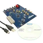
AD9122 Evaluation Board
Quick Start Guide
One Technology Way • P.O. Box 9106 • Norwood, MA 02062-9106, U.S.A. • Tel: 781.329.4700 • Fax: 781.461.3113 • www.analog.com
Getting Started with the AD9122 Evaluation Board
WHAT’S IN THE BOX
EXAMPLE EQUIPMENT LIST
AD9122-M5375-EBZ or AD9122-M5372-EBZ Evaluation Board
Mini-USB Cable
AD9122 Evaluation Board CD
+5Vdc Power Supply: Agilent E3630A
Digital Pattern Generator (DPG2): ADI HSC-DAC-DPG-BZ
DAC Clock Source: R&S SML 02
AQM LO Clock Source: R&S SMA100A
Spectrum Analyzer: Agilent PSAA or R&S FSU
PC: Windows PC with 2 or more USB ports (See Appendix for
system requirements)
INTRODUCTION
The AD9122 Evaluation Board connects to the Analog Devices Digital Pattern Generator (DPG2) to allow for quick evaluation of the
AD9122. The DPG2 allows the user to create many types of digital vectors and transmit these at speed to the AD9122 in any of the
AD9122 operating modes. The AD9122 evaluation board is configured over USB with accompanying PC software.
SOFTWARE INSTALLATION
The AD9122 application software, DPGDownloader, should be installed on the PC prior connecting the hardware to the PC. The DAC
Software Suite is included on the Evaluation Board CD, or can be downloaded from the DPG web site at http://www.analog.com/dpg.
This will install DPGDownloader (for loading vectors into the DPG2) and the AD9122 SPI Controller application.
HARDWARE SETUP (DAC OUTPUT)
Once the DPGDownloader software is installed, the hardware can be connected as shown in Figure 1. A single 5V power supply powers
the evaluation board. The power supply should be able to source up to 2A to cover all of the board’s operating conditions. A low jitter
clock source (< 0.5psec RMS) should be used for the DACCLK. A sinusoidal clock output level of 0 to 4dBm is optimal. By default, the
DAC outputs are connected to SMA connectors for evaluation. Both DAC outputs are available. Later in document, the modifications
for observing the modulator output, and different clocking options will be shown. The evaluation board plugs directly into the DPG2.
The PC connects to both the DPG2 and the evaluation board through USB cables.
Figure 1- Bench Set-Up
Information furnished by Analog Devices is believed to be accurate and reliable. However, no
responsibility is assumed by Analog Devices for its use, nor for any infringements of patents or other
rights of third parties that may result from its use. Specifications subject to change without notice. No
license is granted by implication or otherwise under any patent or patent rights of Analog Devices.
Trademarks and registered trademarks are the property of their respective owners.
Figure 2- DPG2 and AD9122 Evaluation Board
One Technology Way, P.O. Box 9106, Norwood, MA 02062-9106, U.S.A.
Tel: 781.329.4700
www.analog.com
Fax: 781.461.3113
©2009 Analog Devices, Inc. All rights reserved.
�Quick Start Guide
AD9122-EBZ
GETTING STARTED – SINGLE TONE TEST
It is suggested that the basic set-up is verified before making any modifications to the evaluation board.
Basic Hardware Set-Up
Connect the equipment to the AD9122 evaluation board per the following table:
Equipment
Connects to AD9122 Eval Board
Power Supply
P5 (+5V), P6 (GND)
Signal Source
J1 (CLKIN), Set source to 500MHz, 2dBm output
PC USB Cable
XP2
Spectrum Analyzer
J3 (DAC1_P) or J8 (DAC2_P)
DPG2
P1 and P2
DPGDownloader Software
Power up the DPG and connect the USB cable to the PC. Next, run the DPGDownloader Software. A shortcut will be installed to your
Start menu during the installation of the DAC Software Suite. To begin, click on the DPGDownloader shortcut in your Programs menu,
typically at Start > Programs > Analog Devices > DPG > DPGDownloader.
The basic parts of the DPGDownloader window are; Hardware Config Panel, SPI GUI Launch Button, Vector Generation Pull-Down
Menu, Vector Palette, Vector Selection Panel and the Download and Play buttons.
Figure 3 – DPGDownloader Window
©2009 Analog Devices, Inc. All rights reserved. Trademarks and
registered trademarks are the property of their respective owners.
D00000-0-1/07
�Quick Start Guide
AD9122-EBZ
-
If the AD9122 evaluation board has been recognized by the PC, AD9122 should be populated in the Evaluation Board field in
the Hardware Config panel.
-
Generate a sinewave by pulling down the “Add Generated Waveform” menu and choosing “Single Tone”. Fill in the form as
shown in Figure 3 (Sample Rate = 250MHz, Desired Frequency = 29 MHz, etc.). Note that the Sample Rate should match the
input sample rate and not the DAC update rate.
-
Select the I and Q data vectors in the data selection panel.
-
Launch the AD9122 SPI GUI by clicking the AD9122 SPI button. Got to the “Data Clock” tab and change the Interpolation field
to “2x”.
-
When the Run button is clicked, the SPI controller will run once. It will both write and read from the AD9122/AD9125 and
setup the clock chip (AD9516) on the evaluation board. The Run Forever control will setup both the AD9122/AD9125 and
AD9516. This mode of operation will continue to read from the chip and will update the SPI when any of the controls change.
The Force Write and Read Only controls force the controller to write all the controls to the evaluation board or only read from
the SPI port.
-
The DCO frequency field in the DPGDownloader window should now be reading something close to 250MHz.
-
Next hit the download
-
When the vector has finished downloading, hit the play
-
The output from J7 and J8 should be a clean 29MHz tone as shown below:
button. This transfers the data from the PC to the DPG memory.
©2009 Analog Devices, Inc. All rights reserved. Trademarks and
registered trademarks are the property of their respective owners.
D00000-0-1/07
button. This starts the DPG2 transmitting data to the eval board.
�Quick Start Guide
AD9122-EBZ
* RBW 30 kHz
* VBW 100 kHz
Ref
* Att
5 dBm
20 dB
* SWT 160 ms
Marker 1 [T1 ]
0.27 dBm
29.044871795 MHz
1
0
A
1 AP *
AVG
-10
-20
-30
-40
-50 SWP
20 of
20
3DB
-60
-70
-80
-90
Start
1 MHz
Date: 29.SEP.2009
10 MHz/
Stop
101 MHz
13:02:25
Selecting the DAC Outputs
By default, solder jumpers JP4, JP5, JP6, and JP17 configure the AQM output to be observed at SMA output J6. This jumper setting
is shown in Figure 4 b). This connects the DAC outputs to the LPF and the ADL537x analog quadrature modulator. The modulator
LO input can be sourced through SMA connector J15 (LO_IN). The clock level into the modulator should be set to about 3 dBm. In order
to observe the DAC outputs at Jumpers J3 and J8, the solder jumpers need to be repositioned as shown in Figure 4 a).
Figure 4 – a) DAC Output Configuration
©2009 Analog Devices, Inc. All rights reserved. Trademarks and
registered trademarks are the property of their respective owners.
D00000-0-1/07
b) Modulator Output Configuration
�Quick Start Guide
AD9122-EBZ
AD9122 SPI CONTROLLER
The SPI Controller application is split into several tabs. These tabs group related functions. Several of the functions provided by the SPI
Controller are described here, as they relate to the evaluation board. For complete descriptions of each register, refer to the AD9122
datasheet. In the interest of continuous quality improvements, the images below may not exactly match your version of the software.
Data Clock Control
This section, shown in Figure 2, provides control over the Interpolation Rate and Course Modulation. Once the controller is executed, the
Modulation Description field will return a summary of control. If an improper selection is made, the field will return ‘Invalid.’ The
DATAFMT field selects the number format of the incoming data, between unsigned (Binary) and signed (2’s compliment). The QFirst
control selects which DAC receives data first from the interleaved bus. For use with the DPG2, this should always be set to IQ Pairs. The
Interface Mode selects how wide the data bus will be. This setting will need to match the setting in the DPG AD9122 panel for proper
operation with the DPG2.
NCO Control
This tab controls the Fine Modulation within the AD9122. The top portion of this tab helps the user easily control the frequency shift. It
will calculate the NCO Frequency using Data Frequency entered by the user. The NCO can shift the signal by at most +/- fnco/2. An
indicator also displays the frequency shift from the course modulation on the previous tab. The total shift will be the sum of the course
and fine modulations. To manually enter the Frequency Tuning Word (FTW), the Enable Advanced Control will bypass the calculations
on the top of the page.
PLL Control
The AD9122 has an on-chip PLL. When PLL_ENABLE is turned on, the chip will automatically select the appropriate band using the
Divder1 and Divider0 values. This tab provides the calculation for the DAC Freq and VCO Freq based on the Reference Clock and the
value of the dividers. The VCO Frequency must be between 1 and 2 GHz for proper operation. The auto-band select can be bypassed by
enabling PLL MANUAL and entering a band in PLL Band Select. Divider1 and Divider0 must still be chosen appropriately in this mode of
operation.
Interrupts
This tab provides a visual indication of the state of each interrupt. Enabling the button to the left of each interrupt with enable the
interrupt. A green indicator to the right of the button will light when the interrupt is asserted. Once asserted, the interrupt can be
acknowledged by pressing the Clear button.
Main DAC Control
This tab controls the two main DACs in the AD9122. The Full-Scale Current of each DAC can be set with the I DAC Gain and Q DAC
Gain controls. The I Sleep and Q Sleep controls put their respective DAC into a low-power sleep state. When the AD9122 is used with a
modulator, the Phase Compensation/DC Offset controls can be used to correct any mismatches between the two DACs.
©2009 Analog Devices, Inc. All rights reserved. Trademarks and
registered trademarks are the property of their respective owners.
D00000-0-1/07
�Quick Start Guide
AD9122-EBZ
Eval Board Jumper Options
There are 7 pin jumpers on the evaluation board. The pin jumpers are corresponding to the 6 supplies on the board. They serve as
‘switches’ that determine if the LDOs on board or external supplies are used for each individual supply. They are shunted by default,
which means on board LDOs are used. When an external supply is necessary, pull off the shunt from the corresponding supply and
connect the external supply to the SMA jack close to the jumper. The seventh pin jumper configures the voltage of the IOVDD supply.
Table 1 – Pin Jumper configuration Options
Supply Rail
For LDO, Install Pin Jumper
For external Supply, use SMA
CVDD18
JP2
J4
DVDD18
JP3
J11
IOVDD
JP12
J12
AVDD33
JP8
J13
XCVDD33
JP9
J10
AVDD5
JP11
TP11(+5V), TP12 (GND)
©2009 Analog Devices, Inc. All rights reserved. Trademarks and
registered trademarks are the property of their respective owners.
D00000-0-1/07
�Quick Start Guide
AD9122-EBZ
Appendix A – DPGDownloader Notes
Detailed documentation for the DPGDownloader Software and the Full DPG Suite can be accessed thru the Help Pull-down menu. Also
available from the Help pull-down menu is a shortcut for checking to see if there is a more recent DPGDownloader version available with
an option to automatically update the software.
A filter tool that helps users determine the AD9122 interpolation filter is best suited for their application can be launched by clicking the
“Filter Tool” Button on the DPGDownloader main window. The figure below shows the user interface.
©2009 Analog Devices, Inc. All rights reserved. Trademarks and
registered trademarks are the property of their respective owners.
D00000-0-1/07
�