One Technology Way · P.O. Box 9106 · Norwood, MA 02062-9106 · Tel: 781.329.4700 · Fax: 781.461.3113 · www.analog.com
AD9142A-M5372-EBZ Evaluation Board Quick
Start Guide
Getting Started with the AD9142A-M5372-EBZ Evaluation
Board and Software
What's in the Box
●
●
●
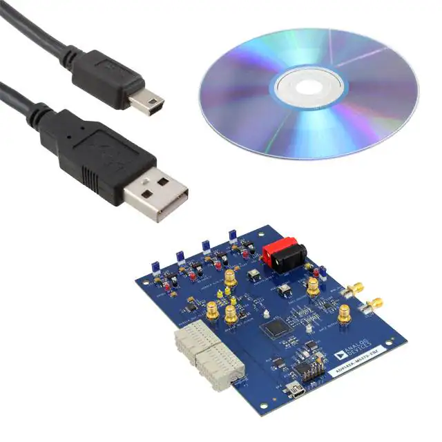
AD9142A-M5372-EBZ Evaluation Board
Evaluation Board CD
Mini-USB Cable
Recommended Equipment List
●
●
●
●
+5Vdc, Power Supply
2 Sinusoidal Clock Sources
Spectrum Analyzer
Data Pattern Generator Series 2 (DPG2)
Introduction
The AD9142A-M5372-EBZ connects to a DPG2 for quick evaluation of the AD9142A, a high-speed,
signal processing Digital to Analog Converter. The DPG2 automatically formats the data and sends it
to the AD9142A-M5372-EBZ, simplifying evaluation of the device. The Evaluation Board (EVB) runs
from a +5V supply. A clock distribution chip AD9516 is included on this EVB as a clock fan-out and
frequency divider for the DACCLK, REFCLK and DPG2 input clock. Also included is a quadrature
modulator ADL5375 for quick DAC+IQMOD evaluation. Figure 2 is an image of the top side of the
AD9142A-M5372-EBZ.
AD9142A Evaluation Software
The AD9142A Evaluation Board software has an easy-to-use graphical user interface (GUI). It is
Rev 07 Aug 2013 10:33 | Page 1
�included on the Evaluation Board CD, or can be downloaded from the DPG website at
http://www.analog.com/dpg. This will install DPGDownloader (for generating and loading vectors into
the DPG2) and AD9142A SPI software.
Hardware Setup
Connect +5.0V to P5, GND to P6. One low phase noise high frequency clock source should be
connected to the SMA connector, J1 (AD9516_CLKIN). The other low phase noise high frequency clock
source should be connected to the SMA connector, J15 (LO_IN), and the spectrum analyzer should be
connected to the SMA connector, J6. The evaluation board connects to the DPG2 through the
connectors P1 and P2. The PC should be connected to the EVB using the mini-USB connector XP2 after
installation of the Evaluation Board software. Figure 1 shows the block diagram of the set-up.
Figure 1. Block diagram of the AD9142A lab bench set-up
Figure 2. Top view of
AD9142A-M5372-EBZ
Getting Started
The PC software comes on the included Evaluation Board CD, but may also be downloaded from the
DPG Web site at http://www.analog.com/dpg. The installation will include the DPG Downloader
software as well as all the necessary AD9142A files including schematic, board layout, datasheet,
AD9142A SPI, and other files.
Initial Set-Up
1. Install the DPG Downloader and AD9142A SPI software and support files on your PC. Follow the
instructions in the installation wizard and use the default (recommended) installation settings.
Rev 07 Aug 2013 10:33 | Page 2
�2. Use a USB cable to connect the EVB to your PC and connect the lab equipment to the EVB.
3. Connect the DGP2 unit to your PC and turn on the unit.
Single-Tone Test
These settings configure the AD9142A to output a sine wave using the DPG2 and allow the user to
view the single-tone performance at the IQMOD output, under the condition: Fdata = 350MHz, 4X
interpolation, IF = 50MHz, LO = 2000MHz, RF = 2050MHz.
1. 1. To begin, open the AD9142A SPI application (Start > All Programs > Analog Devices > SPIPro).
The screen should look similar to Figure 3.
Figure 3 Entry Screen of the AD9142A SPI software
2. Configure the hardware according to the hardware set-up instructions given in the Hardware Setup
section above. Set the frequency of the DAC clock signal generator to 1400MHz, and the output level
to 6dBm. The spectrum analyzer can be configured with Center Frequency = 2050 MHz, Span = 200
MHz, and Resolution Bandwidth of 30 kHz. Choose Input Attenuation to be 24dB. This can be adjusted
later if indications are that the analyzer is causing degradations.
3. Follow the sequence below to configure the AD9142A SPI registers.
Rev 07 Aug 2013 10:33 | Page 3
�a. Click “Reset DAC” button on the “Quick Start” tab.
b. Click “Restore Registers from File” and select the configuration file “Config_8X.csv”. This will
configure the registers with correct values under the condition we are testing.
c. Click “AD9516 Update” button. This step updates the clock distribution chip AD9516 with the
settings that were loaded from the configuration file.
d. There may be a few registers highlighted in red. The red highlights mean mismatches between the
SPI read and write values in the software. Clicking “Read All Registers” reads back all the current
values in the registers, which should resolve the highlights.
e. Toggle register “FIFO SPI RESET REQUEST”. The FIFO level readback registers (INTEGRAL and
FRACTIOANAL) should now match the FIFO level request registers.
f. Open DPG Downloader if you have not done so. (Start > All Programs > Analog Devices > DPG >
DPGDownloader). Ensure that the program detects the AD9142A, as indicated in the “Evaluation
Board” drop-down list, and select it. For this evaluation board, LVDS is the only valid Port
Configuration, and it will be selected automatically. The “DCO Frequency” window should show the
correct data rate (350 MHz). The actual detected frequency may not be exactly 350 MHz but it should
be stable and very close to it as shown in Figure 4.
Figure 4 DPG Downloader Panel
g. Click on “Add Generated Waveform”, and then “Single Tone”. As shown in Figure 5, A Single Tone
panel will be added to the vector list. Enter the sample rate, in this case 350 MHz and the desired
frequency, 50MHz. Enter the digital amplitude. In this case we use -14dBFS. Check the “Generate
Complex Data (I & Q)” box and uncheck the “Unsigned Data” box. Select the In-Phase data vector in
the “I Data Vector” drop down menu and the Quadrature data vector in the “Q Data Vector”.
Rev 07 Aug 2013 10:33 | Page 4
�Figure 5 DPG Downloader sinewave vector
h. Click Download (
) and Play (
).
i. Go back to the AD9142A SPI software and toggle the “FIFO SPI RESET REQUEST” button (from 0 to 1
and back to 0) to reset the FIFO. The FIFO level readback registers (INTEGRAL and FRACTIOANAL)
should now match the FIFO level request registers. The AD9142A SPI software and the spectrum
analyzer should look like Figure 6 and Figure 7 respectively.
Rev 07 Aug 2013 10:33 | Page 5
�Figure 6 Configured Quick Start Tab of the AD9142A SPI software
4. The current on the 5V supply should read about 1310mA.
Rev 07 Aug 2013 10:33 | Page 6
�Figure 7 AD9142A-M5372 Eval Board output Spectrum
SPI SOFTWARE
The AD9142A SPI software is conveniently organized in a series of tabs that groups registers
according to their functions. In this way, all registers associated with the digital functions, for example,
are on the “Digital Functions” tab. All registers associated with the PLL are on the “PLL” tab, and so
on. Normally the “Quick Start” tab is sufficient for a quick evaluation. The most frequently used
register controls are included on this tab. A full description of each register and its settings is given in
the AD9142A data sheet. Some of the registers and their functions are described here as they pertain
to the AD9142A evaluation board. Please note that some of the screen images in this document may
not match exactly with the latest revision of the software, due to ongoing improvements and
enhancements to the software.
The full screen layout is shown in Figure 5. The tabs can be seen across the top of the work area, and
four function buttons in the menu area. “Save Registers to File” and “Restore Registers from File”
allow the user to save the current register settings into a file for later uses. A register is immediately
updated when the value in the control is changed. Switching between tabs does not update register
values. “Read All Registers” can be used to monitor a resister with changing readback values. “
Record Sequence” allows the user to record a series of SPI writes in a particular order and to play
back the sequence later. A short description of the register is shown in the status bar on the bottom
of the work area when the mouse curser hovers over the control. Some of the tabs are discussed
below.
Rev 07 Aug 2013 10:33 | Page 7
�Quick Start
The “Quick Start” tab has selections that apply to the general configuration of the DAC. Reset DAC is
recommended every time when the DAC is powered on or reset. Interpolation Rate allows the user to
select among the 3 interpolation modes (2X, 4X, and 8X). When the NCO is used, set NCO Enable to 1,
fill in the NCO frequency tuning word with the desired value and toggle SPI Update Request. To use
the Fs/4 modulation, turn on the Fs/4 Modulation control. FIFO SPI Reset Request sets the FIFO with
the requested value through a SPI command. The FIFO Level Read Back should reflect the actual FIFO
level after the FIFO SPI Reset Request. Note loading/reloading a vector in the DPG Downloader may
generate glitches on the DCI so it is also recommended to toggle the FIFO SPI RESET REQUEST to
ensure the FIFO level stays optimal. DCI Clk Div Ratio changes the divide ratio of the AD9516 input
clock frequency over DCI frequency. In word mode, this ratio should be the same as the interpolation
rate. In byte mode, it should be half of the interpolation rate. For example, if the interpolation ratio is
4x, the DCI divide ratio should be 2x. Unlike the AD9142A, the AD9516 registers in this SPI software
are not immediately updated after a user changes the value in a control. AD9516 Update loads the
changes in the AD9516 settings.
Figure 8 AD9142A SPI Quick Start tab
PLL
The “PLL” tab includes all the PLL control registers. The recommended settings for the best
performance is PLL Charge Pump Current = 7 and PLL LOOP BW = 7. The user needs to follow the
sequence below to enable the PLL. 1. Choose the desired divide ratios in the Loop Divider and the
Rev 07 Aug 2013 10:33 | Page 8
�VCO Divider.
2. Set PLL Charge Pump Current and PLL Loop BW settings to 7.
3. Set the PLL Mode to Manual.
4. Turn on PLL Enable.
5. Set the PLL Mode to Auto.
Figure 9 AD9142A SPI PLL Tab
EVB Jumper Configurations
This evaluation board allows evaluation of both the DAC IF outputs as well as the modulator RF
outputs. By default, the solder jumpers are configured to look at the modulator RF outputs. Below is a
table listing the jumper configurations and SMA connector connections needed to view either output
on a spectrum analyzer.
Output Viewed
I DAC Output
Q DAC Output
ADL5372 RF Output
SMA Connector
J3(“DAC1 Output”)
J4(“DAC2 Output”)
J6(“MOD_OUT”)
Jumper Configurations
JP4 & JP5 Pins 1-2 (outer pads)
JP6 & JP7 Pins 1-2 (outer pads)
JP4, JP5, JP6, JP7 Pins 2-3 (inner pads)
Note: When viewing the modulator output, a local oscillator (LO) must be connected to J15 (”LO_IN”)
to properly modulate the signals
© Analog Devices, Inc. All rights reserved. Trademarks and
registered trademarks are the property of their respective owners.
www.analog.com
Rev 07 Aug 2013 10:33 | Page 9
�Rev 07 Aug 2013 10:33 | Page 10
�