Quick Start Guide for testing the
AD9250 Analog-to-Digital Converter (ADC) Customer
Evaluation Board Using the FPGA based Capture
Board HSC-ADC-EVALDZ
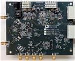
Figure 1: AD9250 Evaluation Board with HSC-ADC-EVALDZ Data Capture Board
Equipment Needed
► Analog signal source and anti-aliasing filter
► Analog Clock Source
► PC
► USB 2.0 port recommended (USB 1.1-compatible)
► AD9250 customer evaluation board
► HSC-ADC-EVALDZ FPGA Based Data Capture Board
Documents Needed
► AD9250 Datasheet
► VisualAnalog Converter Evaluation Tool User Manual, AN-905
► High Speed ADC SPI Control Software User Manual, AN-878
► Interfacing to High Speed ADCs via SPI, AN-877
Software Needed
► VisualAnalog
► SPIController
All documents and software are available at http://www.analog.com/fifo.
1
�For any questions please send an email to highspeed.converters@analog.com.
Install software from the ADI website
1. Download and install VisualAnalog, Rev 1.9.20.21 or later.
2. Download and install SPI Control Software, Rev 1.0.91.3 or later..
Setup hardware and software
1. Connect the AD9250 Customer evaluation board and the HSC-ADC-EVALDZ board
together as shown in Figure 1.
2. Connect one 6V, 2A switching power supply (such as the CUI EPS060250UH-PHP-SZ
supplied) to the AD9250 board. Note: Make sure the 6V power supply is used..
3. Connect one 12V, 3.3A switching power supply (such as the V-Infinity ETSA120330UDCP5P-SZ supplied) to the HSC-ADC-EVALDZ board. Note: Make sure the 12V power
supply is used.
4. Connect the HSC-ADC-EVALDZ board to the PC with a USB cable. (Connect to P702.)
5. On the ADC evaluation board, make sure that jumpers are installed on headers P205, P206,
and P204 for the default setup.
6. On the ADC evaluation board, provide a clean, low jitter clock source to connector J505 at
the desired ADC conversion rate. If the AD9250 input clock divider is used provide a clock
into connector J505 at the appropriate rate which will be divided to your desired clock rate.
The input clock level should be between 10dBm and 14dBm.
7. On the ADC evaluation board, use a clean signal generator with low phase noise to provide
an input signal to the analog input at connector J301 (Channel A) and/or J303 (Channel B).
Use a 1 m, shielded, RG-58, 50 Ω coaxial cable to connect the signal generator. For best
results use a narrow-band, band-pass filter with 50 Ω terminations and an appropriate center
frequency. (ADI uses TTE, Allen Avionics, and K&L band-pass filters.) In order for the
input level to be near the ADC’s full scale, the generator level should be set to 8dBm to
12dBm – this level depends on the input frequency and any losses in bandpass filters.
8. Open VisualAnalog on the PC. “AD9250” should be listed in the status bar of the “New
Canvas” window. Select the template that corresponds to the type of testing that you are
performing. Select the ADC Data Capture Settings window and click on the ‘Capture Board’
tab (see the red box in the figure below). In the FPGA box select the program
“AD9250_12_04_11_1225.mcs” to configure the FPGA. After selecting the file, click the
“Program” button to download the file to the FPGA. The ‘CONFIG_DONE’ LED should
illuminate on the HSC-ADC-EVALDZ board indicating that the FPGA has been correctly
programmed.
2
�9. Next open the SPI Controller software. If prompted for a configuration file, select the
configuration file titled AD9250_14Bit_250MSspiR03.cfg. If not, check the title bar of the
window to see which configuration is loaded. If necessary, choose “Cfg Open” from the
“File” menu and select the configuration files named above. Note that the CHIP ID(1) field
may be filled whether the correct SPI Controller configuration file is loaded or not.
10. In the SPI Controller software, click on File -> MacroGroup Open as shown below.
11. Next, select the file “AD9250_M2L2_SPI.mgp” and click “Open”.
3
�12. To open the macro editor in order to run the macro, select Config -> Launch Macro Group
Editor as shown below:
13. A window should open as shown below:
14. Before running the macro, unplug the power connector to the AD9250 evaluation board and
reconnect it.
15. Click the “Run Macro” button to run the macro as shown below (highlighted in red). This
will configure the AD9250.
4
�16. Click the Run button (
) in VisualAnalog.
17. Adjust the amplitude of the input signal so that the fundamental is at the desired level.
(Examine the “Fund Power” reading in the left panel of the VisualAnalog FFT window.)
18. If desired, click on File>Save Form as in the FFT window to save the FFT plot.
5
�6
�Troubleshooting
► The FFT plot appears abnormal...
If you see a normal noise floor when you disconnect the signal generator from the
analog input, be sure you are not overdriving the ADC. Reduce input level if
necessary.
In VisualAnalog, Click on the Settings button in the “Input Formatter” block. Check
that “Number Format” is set to the correct encoding (2’s compliment by default).
► The FFT plot appears normal, but performance is poor.
Make sure you are using an appropriate filter on the analog input.
Make sure the signal generators for the clock and the analog input are clean (low
phase noise).
If you are using non-coherent sampling, change the analog input frequency slightly.
Make sure the SPI config file matches the product being evaluated.
► The FFT window remains blank after the Run button is clicked.
Make sure the evaluation board is securely connected to the HSC-ADC-EVALDZ
board
Disconnect power from both the ADC evaluation board and the HSC-ADC-EVALDZ
board, disconnect the USB cable from the HSC-ADC-EVALDZ board and begin
again at Step 1.
Make sure the FPGA has been programmed by verifying that the ‘CONFIG_DONE’
LED is illuminated on the HSC-ADC-EVALDZ board.
Make sure the correct FPGA program was installed.
► VisualAnalog indicates that the “FIFO capture timed out.”
Make sure all power and USB connections are secure.
Double check that the encode clock source is present at connector J505.
Revision: 4
7
August 31, 2012
�
很抱歉,暂时无法提供与“AD9250-170EBZ”相匹配的价格&库存,您可以联系我们找货
免费人工找货