16-Bit, 2.5 MHz/5 MHz/10 MHz, 30 MSPS to
160 MSPS Dual Continuous Time Sigma-Delta ADC
AD9262
FEATURES
APPLICATIONS
Baseband quadrature receivers: CDMA2000, W-CDMA,
multicarrier GSM/EDGE, 802.16x, and LTE
Quadrature sampling instrumentation
Medical equipment
Radio detection and ranging (RADAR)
GENERAL DESCRIPTION
The AD9262 is a dual channel, 16-bit analog-to-digital converter (ADC) based on a continuous time (CT) sigma-delta (Σ-Δ)
architecture that achieves −87 dBc of dynamic range over a
10 MHz input bandwidth. The integrated features and characteristics unique to the continuous time Σ-Δ architecture significantly
simplify its use and minimize the need for external components.
FUNCTIONAL BLOCK DIAGRAM
AVDD
DRVDD
ORA
VIN+A
VIN–A
CT Σ-Δ
MODULATOR
VREF
CFILT
VIN–B
VIN+B
CLK+
CLK–
SAMPLE
RATE
CONVERTER
LOW-PASS
DECIMATION
FILTER
AD9262
DC
CORRECT
CMOS
BUFFER
D15A
D0A
QUADRATURE
ERROR
ESTIMATE
GAIN
ADJ
PHASE
ADJ
DCO
CT Σ-Δ
MODULATOR
LOW-PASS
DECIMATION
FILTER
SAMPLE
RATE
CONVERTER
PHASELOCKED
LOOP
DC
CORRECT
CMOS
BUFFER
SERIAL
INTERFACE
AGND
SDIO SCLK CSB
D15B
D0B
ORB
DGND
07772-001
SNR: 83 dB (85 dBFS) to 10 MHz input
SFDR: −87 dBc to 10 MHz input
Noise figure: 15 dB
Input impedance: 1 kΩ
Power: 600 mW
1.8 V analog supply operation
1.8 V to 3.3 V output supply
Selectable bandwidth
2.5 MHz/5 MHz/10 MHz real
5 MHz/10 MHz/20 MHz complex
Output data rate: 30 MSPS to 160 MSPS
Integrated dc and quadrature correction
Integrated decimation filters
Integrated sample rate converter
On-chip PLL clock multiplier
On-chip voltage reference
Offset binary, Gray code, or twos complement data format
Serial control interface (SPI)
Figure 1
The AD9262 incorporates an integrated dc correction and
quadrature estimation block that corrects for gain and phase
mismatch between the two channels. This functional block
proves invaluable in complex signal processing applications
such as direct conversion receivers.
The digital output data is presented in offset binary, Gray code,
or twos complement format. A data clock output (DCO) is
provided to ensure proper timing with the receiving logic. The
AD9262 has the added feature of interleaving Channel A and
Channel B data onto one 16-bit bus, simplifying on-board routing.
The ADC is available in three different bandwidth options of
2.5 MHz, 5 MHz, and 10 MHz, and operates on a 1.8 V analog
supply and a 1.8 V to 3.3 V digital supply, consuming 600 mW.
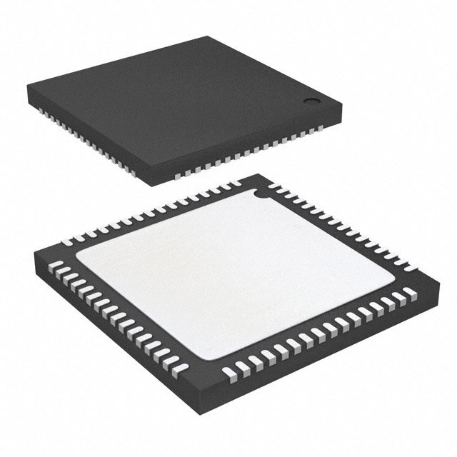
The AD9262 is available in a 64-lead LFCSP and is specified
over the industrial temperature range (−40°C to +85°C).
PRODUCT HIGHLIGHTS
1.
The AD9262 has a resistive input impedance that relaxes the
requirements of the driver amplifier. In addition, a 32× oversampled fifth-order continuous time loop filter significantly attenuates
out-of-band signals and aliases, reducing the need for external
filters at the input.
2.
An external clock input or the integrated integer-N PLL provides
the 640 MHz internal clock needed for the oversampled continuous time Σ-Δ modulator. On-chip decimation filters and sample
rate converters reduce the modulator data rate from 640 MSPS to a
user-defined output data rate between 30 MSPS and 160 MSPS,
enabling a more efficient and direct interface.
4.
3.
5.
6.
Continuous time Σ-Δ architecture efficiently achieves high
dynamic range and wide bandwidth.
Passive input structure reduces or eliminates the requirements for a driver amplifier.
An oversampling ratio of 32× and high order loop filter
provide excellent alias rejection reducing or eliminating the
need for antialiasing filters.
An integrated decimation filter, sample rate converter, PLL
clock multiplier, and voltage reference provide ease of use.
Integrated dc correction and quadrature error correction.
Operates from a single 1.8 V analog power supply and
1.8 V to 3.3 V output supply.
Rev. A
Information furnished by Analog Devices is believed to be accurate and reliable. However, no
responsibility is assumed by Analog Devices for its use, nor for any infringements of patents or other
rights of third parties that may result from its use. Specifications subject to change without notice. No
license is granted by implication or otherwise under any patent or patent rights of Analog Devices.
Trademarks and registered trademarks are the property of their respective owners.
One Technology Way, P.O. Box 9106, Norwood, MA 02062-9106, U.S.A.
Tel: 781.329.4700
www.analog.com
Fax: 781.461.3113
©2010 Analog Devices, Inc. All rights reserved.
�AD9262
TABLE OF CONTENTS
Features .............................................................................................. 1
AD9262BCPZ-10 ....................................................................... 12
Applications ....................................................................................... 1
Equivalent Circuits ......................................................................... 15
General Description ......................................................................... 1
Theory of Operation ...................................................................... 16
Functional Block Diagram .............................................................. 1
Analog Input Considerations ................................................... 16
Product Highlights ........................................................................... 1
Clock Input Considerations ...................................................... 18
Revision History ............................................................................... 2
Power Dissipation and Standby Mode .................................... 20
Specifications..................................................................................... 3
Digital Engine ............................................................................. 21
DC Specifications ......................................................................... 3
DC and Quadrature Error Correction (QEC) ........................ 23
AC Specifications.......................................................................... 4
Digital Outputs ........................................................................... 24
Digital Decimation Filtering Characteristics ............................ 5
Timing ......................................................................................... 25
Digital Specifications ................................................................... 6
Serial Port Interface (SPI) .............................................................. 26
Switching Specifications .............................................................. 7
Configuration Using the SPI ..................................................... 26
Absolute Maximum Ratings............................................................ 8
Hardware Interface..................................................................... 27
Thermal Resistance ...................................................................... 8
Applications Information .............................................................. 28
ESD Caution .................................................................................. 8
Filtering Requirement ................................................................ 28
Pin Configuration and Function Descriptions ............................. 9
Memory Map .................................................................................. 30
Typical Performance Characteristics ........................................... 10
Memory Map Definitions ......................................................... 30
AD9262BCPZ ............................................................................. 10
Outline Dimensions ....................................................................... 32
AD9262BCPZ-5.......................................................................... 11
Ordering Guide .......................................................................... 32
REVISION HISTORY
2/10—Rev. 0 to Rev. A
Changes to Figure 61 ...................................................................... 28
1/10—Revision 0: Initial Version
Rev. A | Page 2 of 32
�AD9262
SPECIFICATIONS
DC SPECIFICATIONS
All power supplies set to 1.8 V, 640 MHz sample rate, 0.5 V internal reference, PLL disabled, 40 MSPS output data rate, AIN1 = −2.0 dBFS,
unless otherwise noted.
Table 1.
Parameter
RESOLUTION
ANALOG INPUT BANDWIDTH
ACCURACY
No Missing Codes
Offset Error
Gain Error
Integral Nonlinearity (INL)2
MATCHING CHARACERISTICS
Offset Error
Gain Error
TEMPERATURE DRIFT
Offset Error
Gain Error
INTERNAL VOLTAGE REFERENCE
ANALOG INPUT
Input Span, VREF = 0.5 V
Common-Mode Voltage
Input Resistance
POWER SUPPLIES
Supply Voltage
AVDD
CVDD
DVDD
DRVDD
Supply Current
IAVDD2
ICVDD2 PLL Enabled
ICVDD2 PLL Disabled
IDVDD2
IDRVDD2 (1.8 V)
IDRVDD2 (3.3 V)
POWER CONSUMPTION
Sine Wave Input2 PLL Disabled
Sine Wave Input2 PLL Enabled
Power-Down Power
Standby Power2
Sleep Power
1
2
Temp
Full
Min
Full
Full
Full
25°C
AD9262BCPZ
Typ
Max
16
2.5
AD9262BCPZ-5
Min
Typ
Max
16
5
AD9262BCPZ-10
Min
Typ
Max
16
10
Guaranteed
±0.025 ±0.2
±0.7
±3.0
±1.5
Guaranteed
±0.025 ±0.2
±0.7
±3.0
±1.5
Guaranteed
±0.025 ±0.2
±0.7
±3.0
±1.5
Full
Full
±0.035
±0.3
Full
Full
±1.5
±50
500
490
±0.2
±1.3
±0.035
±0.3
510
490
±1.5
±50
500
±0.2
±1.3
±0.035
±0.3
510
490
±1.5
±50
500
Unit
Bits
MHz
% FSR
% FSR
LSB
±0.2
±1.3
% FSR
% FSR
510
ppm/°C
ppm/°C
mV
Full
Full
Full
1.7
2
1.8
1
1.9
1.7
2
1.8
1
1.9
1.7
2
1.8
1
1.9
V p-p diff
V
kΩ
Full
Full
Full
Full
1.7
1.7
1.7
1.7
1.8
1.8
1.8
1.8
1.9
1.9
1.9
3.6
1.7
1.7
1.7
1.7
1.8
1.8
1.8
1.8
1.9
1.9
1.9
3.6
1.7
1.7
1.7
1.7
1.8
1.8
1.8
1.8
1.9
1.9
1.9
3.6
V
V
V
V
Full
Full
Full
Full
Full
Full
146
57
8.1
108
8.3
17
165
65
8.8
117
8.6
146
57
8.1
141
8.7
18
165
65
8.8
152
9.1
146
57
8.1
169
10
22
165
65
8.8
182
12.7
mA
mA
mA
mA
mA
mA
Full
Full
Full
Full
Full
487
576
23
10
3
538.5
640
547
636
23
10
3
601.5
703
600
688
23
10
3
660
762
mW
mW
mW
mW
mW
4
4
Input power is referenced to full scale. Therefore, all measurements were taken with a 2 dB signal below full scale, unless otherwise noted.
Measured with a low input frequency, full-scale sine wave.
Rev. A | Page 3 of 32
4
�AD9262
AC SPECIFICATIONS
All power supplies set to 1.8 V, 640 MHz sample rate, 0.5 V internal reference, PLL disabled, 40 MSPS output data rate, AIN = −2.0 dBFS,
unless otherwise noted.
Table 2.
AD9262BCPZ
Parameter1
SIGNAL-TO-NOISE RATIO (SNR)
fIN = 600 kHz2
fIN = 1.2 MHz3
fIN = 2.4 MHz4
fIN = 4.2 MHz
fIN = 8.4 MHz
EFFECTIVE NUMBER OF BITS (ENOB)
fIN = 600 kHz
fIN = 1.2 MHz
fIN = 2.4 MHz
fIN = 4.2 MHz
fIN = 8.4 MHz
SPURIOUS-FREE DYNAMIC RANGE (SFDR)
fIN = 600 kHz2
fIN = 1.2 MHz3
fIN = 2.4 MHz4
fIN = 4.2 MHz
fIN = 8.4 MHz
NOISE SPECTRAL DENSITY (NSD)
AIN = −2 dBFS
AIN = −40 dBFS
NOISE FIGURE5
TWO-TONE SFDR
fIN1 = 1.8 MHz @ −8 dBFS, fIN2 = 2.1 MHz @ −8 dBFS
fIN1 = 2.1 MHz @ −8 dBFS, fIN2 = 2.4 MHz @ −8 dBFS
fIN1 = 3.7 MHz @ −8 dBFS, fIN2 = 4.2 MHz @ −8 dBFS
fIN1 = 7.2 MHz @ −8 dBFS, fIN2 = 8.4 MHz @ −8 dBFS
CROSSTALK6
ANALOG INPUT BANDWIDTH
APERTURE JITTER
Temp
Min
Typ
Full
Full
Full
25°C
25°C
86
89
89
89
25°C
25°C
25°C
25°C
25°C
Max
14.5
14.5
AD9262BCPZ-5
Min
Typ
83
86
86
86
Max
AD9262BCPZ-10
Min
81
14
14
Full
Full
Full
25°C
25°C
−87
−87
0
>0
Rev. A | Page 25 of 32
Description
Digital trip: if 16-bit output > 32,767, ORx = 1, else ORx = 0
Digital threshold: if 16-bit output > ORTHRESH, ORx = 1,
else ORx = 0
If analog trip or digital trip, ORx = 1, else ORx = 0
�AD9262
SERIAL PORT INTERFACE (SPI)
During an instruction phase, a 16-bit instruction is transmitted.
Data follows the instruction phase, and the length is determined
by the W0 bit and the W1 bit. All data is composed of 8-bit words.
The first bit of each individual byte of serial data indicates whether
a read or write command is issued. This allows the serial data
input/output (SDIO) pin to change direction from an input to
an output.
The AD9262 serial port interface (SPI) allows the user to configure
the converter for specific functions or operations through a
structured register space provided inside the ADC. This provides
the user added flexibility and customization depending on the
application. Addresses are accessed via the serial port and can
be written to or read from via the port. Memory is organized
into bytes that are further divided into fields, as documented in
the Memory Map section. For detailed operational information,
see the AN-877 Application Note, Interfacing to High Speed
ADCs via SPI.
In addition to word length, the instruction phase determines if
the serial frame is a read or write operation, allowing the serial
port to be used to both program the chip and to read the contents
of the on-chip memory. If the instruction is a readback operation, performing a readback causes the serial data input/output
(SDIO) pin to change direction from an input to an output at the
appropriate point in the serial frame.
CONFIGURATION USING THE SPI
As summarized in Table 22, three pins define the SPI of this ADC.
The SCLK pin synchronizes the read and write data presented
to the ADC. The SDIO pin allows data to be sent and read from
the internal ADC memory map registers. The CSB pin is an active
low control that enables or disables the read and write cycles.
Table 22. Serial Port Interface Pins
Data can be sent in MSB-first or in LSB-first mode. MSB first is
the default setting on power-up and can be changed via the
configuration register. For more information, see the AN-877
Application Note, Interfacing to High Speed ADCs via SPI.
Pin Name
SCLK
Table 23. SPI Timing Diagram Specifications
SDIO
CSB
Description
SCLK (serial clock) is the serial shift clock. SCLK
synchronizes serial interface reads and writes.
SDIO (serial data input/output) is an input and
output depending on the instruction being sent
and the relative position in the timing frame.
CSB (chip select bar) is an active low control that
gates the read and write cycles.
Parameter
tSDS
tSDH
tSCLK
tSS
tSH
tSHIGH
The falling edge of CSB in conjunction with the rising edge of
SCLK determines the start of the framing. Figure 60 and Table 23
provide an example of the serial timing and its definitions.
Description
Setup time between data and rising edge of SCLK
Hold time between data and rising edge of SCLK
Period of the clock
Setup time between CSB and SCLK
Hold time between CSB and SCLK
Minimum period that SCLK should be in a logic
high state
Minimum period that SCLK should be in a logic
low state
tSLOW
Other modes involving CSB are available. CSB can be held low
indefinitely to permanently enable the device (this is called
streaming). CSB can stall high between bytes to allow for additional external timing. When CSB is tied high, SPI functions are
placed in a high impedance mode.
tSDS
tSS
tSHIGH
tSDH
tSCLK
tSH
tSLOW
CSB
SCLK DON’T CARE
R/W
W1
W0
A12
A11
A10
A9
A8
A7
D5
D4
D3
D2
D1
D0
DON’T CARE
07772-054
SDIO DON’T CARE
DON’T CARE
Figure 60. Serial Port Interface Timing Diagram
Rev. A | Page 26 of 32
�AD9262
HARDWARE INTERFACE
The pins described in Table 22 comprise the physical interface
between the programming device of the user and the serial port
of the AD9262. The SCLK and CSB pins function as inputs
when using the SPI interface. The SDIO pin is bidirectional,
functioning as an input during write phases and as an output
during readback.
The SPI interface is flexible enough to be controlled by either
PROM or PIC microcontrollers. This provides the user with the
ability to use an alternate method to program the ADC. One
such method is described in detail in the AN-812 Application
Note, MicroController-Based Serial Port Interface (SPI) Boot
Circuit.
Rev. A | Page 27 of 32
�AD9262
APPLICATIONS INFORMATION
Depending on the application and the system architecture, this
low order filter may or may not be necessary. The signal transfer function (STF) of a continuous time feedforward ADC
usually contains out-of-band peaks. Because these STF peaks
are typically one or two octaves above the pass-band edge, they
are not problematic in applications where the bulk of the signal
energy is in or near the pass band. However, in applications
with large far-out interferers, it is necessary to either add a filter
to attenuate these problematic signals or to allocate some of the
ADC dynamic range to accommodate them.
Figure 61 shows the normalized STF of the AD9262 CT Σ-Δ
converter. The figure shows out-of-band peaking beyond the
band edge of the ADC. Within the 10 MHz band of interest, the
STF is maximally flat with less than 0.1 dB of gain. Maximum
peaking occurs at 60 MHz with 10 dB of gain. To put this into
perspective, for a fixed input power, a 5 MHz in-band signal
appears at −5 dBFS, a 25 MHz tone appears at −2 dBFS and
60 MHz tone at +5 dBFS. Because the maximum input to the
ADC is −2 dBFS, large out-of-band signals can quickly saturate
the system. This implies that, under these conditions, the digital
outputs of the ADC no longer accurately represent the input.
See the Overrange (OR) Condition section for details on overrange detection and recovery.
15
13
The noise performance is normalized to a −2 dBFS in-band
signal. The AD9262 STF and NTF are flat within the band of
interest and should result in almost no change in input level
and IBN. Beyond the bandwidth of the AD9262, out-of-band
peaking adds gain to the system, therefore requiring the input
power to be scaled back to prevent in-band noise degradation.
The input power is scaled back to a point where only 3 dB of
noise degradation is allowed, therefore resulting in the response
shown in Figure 62.
5
0
–5
–40°C
–10
–15
+85°C
+25°C
CHEBYSHEVII
FILTER RESPONSE
–20
–25
0
10
20
30
40
50
80
90
100
An example third-order, low-pass Chebyshev II type filter is
shown in Figure 63. Table 24 summarizes the components
and manufacturers used to build the circuit.
L1
180nH
9
C1
18pF
5
C2
390pF
L1
180nH
3
1
VIN+
C3
150pF
1kΩ
AD9262
CT-Σ-Δ
VIN–
C2
390pF
–1
Figure 63. Third-Order, Low-Pass Chebyshev II Filter
–3
0
10
20
30
40
50
60
FREQUENCY (MHz)
70
80
90
100
Figure 61. STF
Rev. A | Page 28 of 32
07772-095
7
07772-073
GAIN (dB)
70
Figure 62. Maximum Input Level for 3 dB Noise Degradation
11
–5
60
FREQUENCY (MHz)
07772-074
The need for antialias protection often requires one or two
octaves for a transition band, which reduces the usable bandwidth of a Nyquist converter to between 25% and 50% of the
available bandwidth. A CT Σ-Δ converter maximizes the available signal bandwidth by forgoing the need for an anti-aliasing
filter because the architecture possesses inherent anti-aliasing.
Although a high order, sharp cutoff antialiasing filter may not
be necessary because of the unique characteristics of the
architecture, a low order filter may still be required to precede
the ADC for out-of-band signal handling.
Figure 61 shows the gain profile of the AD9262, and this can be
interpreted as the level at which the signal power should be
scaled back to prevent an overload condition. This is the ultimate trip point and before this point is reached, the in-band
noise (IBN) slowly degrades. As a result, it is recommended that
the low-pass filter be designed to match the profile of Figure 62,
which shows the maximum input signal for a 3 dB degradation
of in-band noise. The input signal is attenuated to allow only
3 dB of noise degradation over frequency.
AMPLITUDE (dB)
FILTERING REQUIREMENT
�AD9262
Table 24. Chebyshev II Filter Components
Parameter
C1
L1
C2
C3
Value
18
180
390
150
Unit
pF
nH
pF
pF
Manufacturer
Murata GRM188 series, 0603
Coil Craft 0603 LS, 2%
Murata GRM188 series, 0603
Murata GRM188 series, 0603
In addition to matching the profile of Figure 62, group delay
and channel matching are important filter design criteria. Low
tolerance components are highly recommended for improved
channel matching, which translates to minimal degradation in
image rejection for quadrature systems.
Rev. A | Page 29 of 32
�AD9262
MEMORY MAP
Table 25. Memory Map
Register Name
SPI Port Config
Chip ID
Chip Grade
Channel Index
Power Modes
PLLENABLE
PLL
Analog Input
Output Modes
Output Adjust
Output Clock
Reference
Output Data
Overrange
QEC1
QEC2
Address
0x00
0x01
0x02
0x05
0x08
0x09
0x0A
0x0F
0x14
0x15
0x16
0x18
0x101
0x111
0x112
0x113
Bit 7
0
Bit 6
LSBFIRST
Bit 5
SOFTRESET
Bit 4
Bit 3
1
1
CHIPID[7:0]
CHILDID[2:0]
1
Bit 2
SOFTRESET
Bit 1
LSBFIRST
Channel[1:0]
PWRDWN[1:0]
PLLLOCKED
DRVSTD
PLLENABLE
PLLMULT[5:0]
PLLAUTO
BW[1:0]
Interleave
OUTENB
OUTINV
DRVSTR33[1:0]
Format[1:0]
DRVSTR18[1:0]
DCOINV
AUTORST
EXTREF
QEC
OR_IND
DCFRZ
PHASEFRZ
KOUT[5:0]
ORTHRESH[5:0]
GAINFRZ
DCENB
DCFRC
PHASEENB
PHASEFRC
MEMORY MAP DEFINITIONS
Table 26. Memory Map Definitions
Register
SPI Port Config
Address
0x00
Bit(s)
6, 1
Mnemonic
LSBFIRST
Default
0
Chip ID
Chip Grade
0x01
0x02
5, 2
[7:0]
[5:4]
SOFTRESET
CHIPID
CHILDID
0
0x22
0
Channel Index
0x05
[1:0]
Channel
0
Power Modes
0x08
[1:0]
PWRDWN
0
PLLENABLE
PLL
0x09
0x0A
2
7
PLLENABLE
PLLLOCKED
0
0
0x0F
6
[5:0]
[6:5]
PLLAUTO
PLLMULT
BW
0
0
0
Analog Input
Bit 0
0
Description
0: serial interface uses MSB first format
1: serial interface uses LSB first format
1: default all serial registers except 0x00, 0x09, and 0x0A
0x22: AD9262
0x00: 10 MHz bandwidth
0x10: 5 MHz bandwidth
0x20: 2.5 MHz bandwidth
0: both channels addressed simultaneously
1: Channel A only addressed
2: Channel B only addressed
3: both channels addressed simultaneously
0x0: normal operation
0x1: power-down (local)
0x2: standby (everything except reference circuits)
0x3: sleep
1: enable PLL
0: PLL is not locked
1: PLL is locked
1: PLL autoband enabled
See Table 10
See Table 13
Rev. A | Page 30 of 32
GAINENB
GAINFRC
�AD9262
Register
Output Modes
Output Adjust
Address
0x14
0x15
Output Clock
Reference
Output Data
0x16
0x18
0x101
Overrange
0x111
QEC1
0x112
QEC2
0x113
Bit(s)
7
Mnemonic
DRVSTD
Default
0
5
4
2
[1:0]
Interleave
OUTENB
OUTINV
Format
0
0
0
0
[3:2]
DRVSTR33
0
[1:0]
DRVSTR18
2
7
6
6
[5:0]
7
6
[5:0]
5
4
3
2
1
0
2
1
0
DCOINV
EXTREF
QEC
KOUT
AUTORST
OR_IND
ORTHRESH
DCFRZ
PHASEFRZ
GAINFRZ
DCENB
PHASEENB
GAINENB
DCFRC
PHASEFRC
GAINFRC
0
0
0
0
0
0
0
0
0
0
0
0
0
0
0
0
Description
0: 3.3 V
1: 1.8 V
1: interleave both channels onto D[15:0]A
1: data outputs tristated
1: data outputs bitwise inverted
0: offset binary
1: twos complement
2: Gray code
3: offset binary
Typical output sink current to DGND
0: 33 mA
1: 63 mA
2: 93 mA
3: 120 mA
Typical output sink current to DGND
0: 10 mA
1: 20 mA
2: 30 mA
3: 39 mA
1: invert DCO
1: use external reference
1: enable quadrature error correction
Output data rate, see Table 18
1: enable loop filter reset indicator on ORx pin
Refer to Table 21
Refer to Table 20
1: freeze dc correction coefficients
1: freeze phase correction coefficients
1: freeze gain correction coefficients
1: disable dc correction
1: disable phase correction
1: disable gain correction
1: force dc correction coefficients to initial static values
1: force phase correction coefficients to initial static values
1: force gain correction coefficients to initial static values
Rev. A | Page 31 of 32
�AD9262
OUTLINE DIMENSIONS
0.60 MAX
9.00
BSC SQ
0.60
MAX
48
64
49
PIN 1
INDICATOR
1
PIN 1
INDICATOR
0.50
BSC
0.50
0.40
0.30
1.00
0.85
0.80
SEATING
PLANE
33
32
16
17
0.05 MAX
0.02 NOM
0.30
0.23
0.18
0.25 MIN
7.50
REF
0.80 MAX
0.65 TYP
12° MAX
6.35
6.20 SQ
6.05
EXPOSED PAD
(BOTTOM VIEW)
0.20 REF
FOR PROPER CONNECTION OF
THE EXPOSED PAD, REFER TO
THE PIN CONFIGURATION AND
FUNCTION DESCRIPTIONS
SECTION OF THIS DATA SHEET.
COMPLIANT TO JEDEC STANDARDS MO-220-VMMD-4
091707-C
8.75
BSC SQ
TOP VIEW
Figure 64. 64-Lead Lead Frame Chip Scale Package [LFCSP_VQ]
9 mm × 9 mm Body, Very Thin Quad
(CP-64-4)
Dimensions shown in millimeters
ORDERING GUIDE
Model1
AD9262BCPZ-10
AD9262BCPZ-5
AD9262BCPZ
AD9262EBZ
AD9262-5EBZ
AD9262-10EBZ
1
Temperature Range
−40°C to +85°C
−40°C to +85°C
−40°C to +85°C
Package Description
64-Lead Lead Frame Chip Scale Package [LFCSP_VQ]
64-Lead Lead Frame Chip Scale Package [LFCSP_VQ]
64-Lead Lead Frame Chip Scale Package [LFCSP_VQ]
Evaluation Board
Evaluation Board
Evaluation Board
Z = RoHS Compliant Part.
©2010 Analog Devices, Inc. All rights reserved. Trademarks and
registered trademarks are the property of their respective owners.
D07772-0-2/10(A)
Rev. A | Page 32 of 32
Package Option
CP-64-4
CP-64-4
CP-64-4
�


 工商网监
湘ICP备2023018690号
工商网监
湘ICP备2023018690号
