AD9288BST-40

AD9288BST-40

  • 厂商:

    AD(亚德诺)

  • 封装:

  • 描述:

    AD9288BST-40 - 8-Bit, 40/80/100 MSPS Dual A/D Converter - Analog Devices

  • 详情介绍
  • 数据手册
  • 价格&库存
AD9288BST-40 数据手册
a FEATURES Dual 8-Bit, 40 MSPS, 80 MSPS, and 100 MSPS ADC Low Power: 90 mW at 100 MSPS per Channel On-Chip Reference and Track/Holds 475 MHz Analog Bandwidth Each Channel SNR = 47 dB @ 41 MHz 1 V p-p Analog Input Range Each Channel Single +3.0 V Supply Operation (2.7 V–3.6 V) Standby Mode for Single Channel Operation Twos Complement or Offset Binary Output Mode Output Data Alignment Mode APPLICATIONS Battery Powered Instruments Hand-Held Scopemeters Low Cost Digital Oscilloscopes I and Q Communications ENCA AINA AINA REFINA REFOUT REFINB AINB AINB ENCB 8-Bit, 40/80/100 MSPS Dual A/D Converter AD9288 FUNCTIONAL BLOCK DIAGRAM VDD TIMING OUTPUT REGISTER AD9288 T/H ADC 8 8 D7A–D0A SELECT #1 SELECT #2 REF OUTPUT REGISTER DATA FORMAT SELECT 8 D7B–D0B T/H ADC 8 TIMING VD GND VDD GENERAL DESCRIPTION The AD9288 is a dual 8-bit monolithic sampling analog-todigital converter with on-chip track-and-hold circuits and is optimized for low cost, low power, small size and ease of use. The product operates at a 100 MSPS conversion rate with outstanding dynamic performance over its full operating range. Each channel can be operated independently. The ADC requires only a single 3.0 V (2.7 V to 3.6 V) power supply and an encode clock for full-performance operation. No external reference or driver components are required for many applications. The digital outputs are TTL/CMOS compatible and a separate output power supply pin supports interfacing with 3.3 V or 2.5 V logic. The encode input is TTL/CMOS compatible and the 8-bit digital outputs can be operated from +3.0 V (2.5 V to 3.6 V) supplies. User-selectable options are available to offer a combination of standby modes, digital data formats and digital data timing schemes. In standby mode, the digital outputs are driven to a high impedance state. Fabricated on an advanced CMOS process, the AD9288 is available in a 48-lead surface mount plastic package (7 × 7 mm, 1.4 mm LQFP) specified over the industrial temperature range (–40°C to +85°C). R EV. 0 Information furnished by Analog Devices is believed to be accurate and reliable. However, no responsibility is assumed by Analog Devices for its use, nor for any infringements of patents or other rights of third parties which may result from its use. No license is granted by implication or otherwise under any patent or patent rights of Analog Devices. One Technology Way, P.O. Box 9106, Norwood, MA 02062-9106, U.S.A. Tel: 781/329-4700 World Wide Web Site: http://www.analog.com Fax: 781/326-8703 © Analog Devices, Inc., 1999 AD9288–SPECIFICATIONS (V Parameter RESOLUTION DC ACCURACY Differential Nonlinearity Integral Nonlinearity No Missing Codes Gain Error1 Gain Tempco1 Gain Matching Voltage Matching ANALOG INPUT Input Voltage Range (With Respect to AIN) Common-Mode Voltage Input Offset Voltage Reference Voltage Reference Tempco Input Resistance Input Capacitance Analog Bandwidth, Full Power SWITCHING PERFORMANCE Maximum Conversion Rate Minimum Conversion Rate Encode Pulsewidth High (tEH) Encode Pulsewidth Low (tEL) Aperture Delay (tA) Aperture Uncertainty (Jitter) Output Valid Time (tV)2 Output Propagation Delay (tPD)2 DIGITAL INPUTS Logic “1” Voltage Logic “0” Voltage Logic “1” Current Logic “0” Current Input Capacitance DIGITAL OUTPUTS Logic “1” Voltage Logic “0” Voltage 3 DD = 3.0 V; VD = 3.0 V, Differential Input; External reference unless otherwise noted.) AD9288BST-80 Min Typ Max 8 +1.25 +1.50 +1.25 +1.50 –6 –8 ± 0.5 ± 0.50 +1.25 +1.50 +1.25 +1.50 –6 –8 AD9288BST-40 Min Typ Max 8 ± 0.5 ± 0.50 +1.25 +1.50 +1.25 +1.50 Units Bits LSB LSB LSB LSB % FS % FS ppm/°C % FS mV Temp Test Level AD9288BST-100 Min Typ Max 8 +25°C Full +25°C Full Full +25°C Full Full +25°C +25°C I VI I VI VI I VI VI V V ± 0.5 ± 0.50 –6 –8 Guaranteed ± 2.5 +6 +8 80 ± 1.5 ± 15 Guaranteed ± 2.5 +6 +8 80 ± 1.5 ± 15 Guaranteed ± 2.5 +6 +8 80 ± 1.5 ± 15 Full Full +25°C Full Full Full +25°C Full +25°C +25°C Full +25°C +25°C +25°C +25°C +25°C Full Full Full Full Full Full +25°C Full Full Full Full +25°C +25°C +25°C +25°C +25°C +25°C V V I VI VI VI I VI V V VI IV IV IV V V VI VI VI VI VI VI V VI VI VI VI I V V –35 1.2 7 5 ± 512 ± 200 ± 10 ± 40 1.25 ± 130 10 2 475 +35 1.3 13 16 –35 1.2 7 5 ± 512 ± 200 ± 10 ± 40 1.25 ± 130 10 2 475 +35 1.3 13 16 –35 1.2 7 5 ± 512 ± 200 ± 10 ± 40 1.25 ± 130 10 2 475 +35 1.3 13 16 mV p-p mV mV mV V ppm/°C kΩ kΩ pF MHz MSPS MSPS ns ns ns ps rms ns ns V V µA µA pF V V mW mW mV/V ns ns 100 4.3 4.3 0 5 3.0 4.5 2.0 0.8 ±1 ±1 2.0 2.45 0.05 180 6 8 2 2 218 11 20 1 1000 1000 80 5.0 5.0 0 5 3.0 4.5 2.0 0.8 ±1 ±1 2.0 2.45 0.05 171 6 8 2 2 207 11 20 1 1000 1000 40 8.0 8.0 0 5 3.0 4.5 2.0 0.8 ±1 ±1 2.0 2.45 0.05 156 6 8 2 2 189 11 20 1 1000 1000 POWER SUPPLY Power Dissipation4 Standby Dissipation4, 5 Power Supply Rejection Ratio (PSRR) DYNAMIC PERFORMANCE Transient Response Overvoltage Recovery Time Signal-to-Noise Ratio (SNR) (Without Harmonics) fIN = 10.3 MHz fIN = 26 MHz fIN = 41 MHz 6 I I I 44 47.5 47.5 47.0 44 47.5 47 44 47.5 dB dB dB –2– REV. 0 AD9288 Parameter 6 Temp Test Level AD9288BST-100 Min Typ Max AD9288BST-80 Min Typ Max AD9288BST-40 Min Typ Max Units DYNAMIC PERFORMANCE (Continued) Signal-to-Noise Ratio (SINAD) (With Harmonics) fIN = 10.3 MHz +25°C I fIN = 26 MHz +25°C I fIN = 41 MHz +25°C I Effective Number of Bits fIN = 10.3 MHz +25°C I fIN = 26 MHz +25°C I +25°C I fIN = 41 MHz 2nd Harmonic Distortion +25°C I fIN = 10.3 MHz fIN = 26 MHz +25°C I +25°C I fIN = 41 MHz 3rd Harmonic Distortion +25°C I fIN = 10.3 MHz fIN = 26 MHz +25°C I +25°C I fIN = 41 MHz Two-Tone Intermod Distortion (IMD) fIN = 10.3 MHz +25°C V 44 47 47 47 7.5 7.5 7.5 70 70 70 60 60 60 60 44 47 47 47 7.5 7.5 7.5 70 70 70 60 60 60 60 44 47 dB dB dB Bits Bits Bits dBc dBc dBc dBc dBc dBc dBc 7.0 7.5 7.0 7.0 55 70 55 55 55 60 55 52 60 NOTES 1 Gain error and gain temperature coefficient are based on the ADC only (with a fixed 1.25 V external reference). 2 tV and t PD are measured from the 1.5 V level of the ENCODE input to the 10%/90% levels of the digital outputs swing. The digital output load during test is not to exceed an ac load of 10 pF or a dc current of ± 40 µA. 3 Digital supply current based on V DD = +3.0 V output drive with
AD9288BST-40
物料型号: - 型号:AD9288 - 
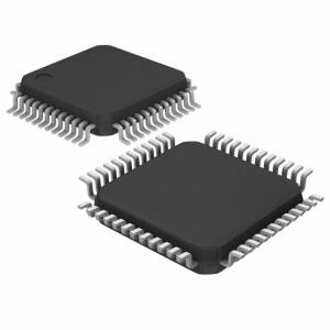
封装:48-lead LQFP (ST-48)

器件简介: - AD9288是一款双8位单片采样模拟至数字转换器(ADC),内置跟踪保持电路,专为低成本、低功耗、小尺寸和易用性而优化。产品以100 MSPS的转换率运行,在全操作范围内具有出色的动态性能。每个通道可以独立操作。

引脚分配: - GND:接地引脚(Pin No. 1, 12, 16, 27, 29, 32, 34, 45) - AINA/ANA:通道A的模拟输入及其互补端(Pin No. 2, 3) - DFS:数据格式选择(Pin No. 4) - REFINA/REFINB:通道A和B的参考电压输入(Pin No. 5, 7) - S1/S2:用户选择选项1和2(Pin No. 8, 9) - ANB/AINB:通道B的模拟输入及其互补端(Pin No. 10, 11) - VD/VDD:模拟/数字电源(Pin No. 13, 30, 31, 48 / Pin No. 15, 28, 33, 46) - D7B-D0B/DOA-D7A:通道B和A的数字输出(Pin No. 17-24 / Pin No. 37-44) - ENCA/ENCB:通道A和B的时钟输入(Pin No. 47 / Pin No. 14)

参数特性: - 8-Bit, 40/80/100 MSPS双ADC - 低功耗:每通道100 MSPS时90 mW - 每个通道475 MHz模拟带宽 - 信噪比(SNR)= 47 dB @ 41 MHz - 1 V p-p模拟输入范围 - 单+3.0 V供电操作(2.7 V–3.6 V) - 待机模式下单通道操作

功能详解: - AD9288 ADC架构是每位流水线型转换器,使用开关电容技术。这些阶段决定了5位MSB,并驱动一个3位的闪存。每个阶段提供了足够的重叠和误差校正,允许比较器精度优化。 - 输入缓冲器是差分的,两组输入都在内部偏置,允许最灵活的交流或直流以及差分或单端输入模式使用。 - 输出缓冲器从单独的电源供电,允许调整输出电压摆动。

应用信息: - 电池供电仪器、手持示波器、低成本数字示波器、I和Q通信等应用。

封装信息: - 48引脚表面贴装塑料封装(7 × 7 mm,1.4 mm LQFP),工业温度范围(–40°C至+85°C)。
AD9288BST-40 价格&库存

很抱歉,暂时无法提供与“AD9288BST-40”相匹配的价格&库存,您可以联系我们找货

免费人工找货
AD9288BSTZ-100
  •  国内价格
  • 1+56.4435
  • 10+54.353
  • 100+49.3358
  • 500+46.8272

库存:0