FUNCTIONAL BLOCK DIAGRAM
APPLICATIONS
Low jitter, low phase noise clock distribution
Clock generation and translation for SONET, 10Ge, 10G FC,
and other 10 Gbps protocols
Forward error correction (G.710)
Clocking high speed ADCs, DACs, DDSs, DDCs, DUCs, MxFEs
High performance wireless transceivers
ATE and high performance instrumentation
Broadband infrastructures
GENERAL DESCRIPTION
The AD9522-01 provides a multioutput clock distribution
function with subpicosecond jitter performance, along with an
on-chip PLL and VCO. The on-chip VCO tunes from 2.53 GHz
to 2.95 GHz. An external 3.3 V/5 V VCO/VCXO of up to 2.4 GHz
can also be used.
1
CP
OPTIONAL
REF1
REFIN
REFIN
CLK
REF2
LF
STATUS
MONITOR
PLL
Low phase noise, phase-locked loop (PLL)
On-chip voltage controlled oscillator (VCO) tunes from
2.53 GHz to 2.95 GHz
Supports external 3.3 V/5 V VCO/VCXO to 2.4 GHz
1 differential or 2 single-ended reference inputs
Accepts CMOS, LVPECL, or LVDS references to 250 MHz
Accepts 16.62 MHz to 33.3 MHz crystal for reference input
Optional reference clock doubler
Reference monitoring capability
Revertive automatic and manual reference switchover/
holdover modes
Glitch-free switchover between references
Automatic recovery from holdover
Digital or analog lock detect, selectable
Optional zero delay operation
Twelve 800 MHz LVDS outputs divided into 4 groups
Each group of 3 has a 1-to-32 divider with phase delay
Additive output jitter as low as 242 fs rms
Channel-to-channel skew grouped outputs < 60 ps
Each LVDS output can be configured as 2 CMOS outputs
(for fOUT ≤ 250 MHz)
Automatic synchronization of all outputs on power-up
Manual synchronization of outputs as needed
SPI- and I²C-compatible serial control port
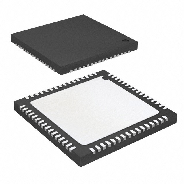
64-lead LFCSP
Nonvolatile EEPROM stores configuration settings
VCO
ZERO
DELAY
DIVIDER
AND MUXES
LVDS/
CMOS
DIV/Φ
OUT0
OUT1
OUT2
DIV/Φ
OUT3
OUT4
OUT5
DIV/Φ
OUT6
OUT7
OUT8
DIV/Φ
OUT9
OUT10
OUT11
SPI/I2C CONTROL
PORT AND
DIGITAL LOGIC
EEPROM
AD9522
07219-001
FEATURES
SWITCHOVER
AND MONITOR
Data Sheet
12 LVDS/24 CMOS Output Clock Generator
with Integrated 2.8 GHz VCO
AD9522-0
Figure 1.
The AD9522 serial interface supports both SPI and I²C® ports.
An in-package EEPROM can be programmed through the
serial interface and store user-defined register settings for
power-up and chip reset.
The AD9522 features 12 LVDS outputs in four groups. Any of
the 800 MHz LVDS outputs can be reconfigured as two
250 MHz CMOS outputs.
Each group of outputs has a divider that allows both the divide
ratio (from 1 to 32) and the phase (coarse delay) to be set.
The AD9522 is available in a 64-lead LFCSP and can be operated
from a single 3.3 V supply. The external VCO can have an
operating voltage up to 5.5 V.
The AD9522 is specified for operation over the standard industrial
range of −40°C to +85°C.
The AD9520-0 is an equivalent part to the AD9522-0 featuring
LVPECL/CMOS drivers instead of LVDS/CMOS drivers.
The AD9522 is used throughout this data sheet to refer to all the members of the AD9522 family. However, when AD9522-0 is used, it is referring to that specific
member of the AD9522 family.
Rev. A
Document Feedback
Information furnished by Analog Devices is believed to be accurate and reliable. However, no
responsibility is assumed by Analog Devices for its use, nor for any infringements of patents or other
rights of third parties that may result from its use. Specifications subject to change without notice. No
license is granted by implication or otherwise under any patent or patent rights of Analog Devices.
Trademarks and registered trademarks are the property of their respective owners.
One Technology Way, P.O. Box 9106, Norwood, MA 02062-9106, U.S.A.
Tel: 781.329.4700 ©2008–2015 Analog Devices, Inc. All rights reserved.
Technical Support
www.analog.com
�AD9522-0
Data Sheet
TABLE OF CONTENTS
Features .............................................................................................. 1
Mode 1: Clock Distribution or External VCO < 1600 MHz
.................................................................................................. 31
Applications ....................................................................................... 1
Mode 2: High Frequency Clock Distribution—CLK or
External VCO > 1600 MHz .................................................. 33
General Description ......................................................................... 1
Functional Block Diagram .............................................................. 1
Phase-Locked Loop (PLL) .................................................... 35
Revision History ............................................................................... 4
Configuration of the PLL ...................................................... 35
Specifications..................................................................................... 5
Phase Frequency Detector (PFD) ........................................ 35
Power Supply Requirements ....................................................... 5
Charge Pump (CP) ................................................................. 35
PLL Characteristics ...................................................................... 5
On-Chip VCO ........................................................................ 36
Clock Inputs .................................................................................. 8
PLL External Loop Filter ....................................................... 36
Clock Outputs ............................................................................... 8
PLL Reference Inputs ............................................................. 36
Timing Characteristics ................................................................ 9
Reference Switchover ............................................................. 37
Timing Diagrams ..................................................................... 9
Reference Divider R ............................................................... 37
Clock Output Additive Phase Noise (Distribution Only; VCO
Divider Not Used) ...................................................................... 10
VCO/VCXO Feedback Divider N: P, A, B .......................... 37
Clock Output Absolute Phase Noise (Internal VCO Used) .. 11
Digital Lock Detect (DLD) ................................................... 39
Clock Output Absolute Time Jitter (Clock Generation Using
Internal VCO) ............................................................................. 11
Analog Lock Detect (ALD)................................................... 39
Clock Output Absolute Time Jitter (Clock Cleanup Using
Internal VCO) ............................................................................. 11
External VCXO/VCO Clock Input (CLK/CLK) ................ 40
Current Source Digital Lock Detect (CSDLD) .................. 39
Holdover .................................................................................. 40
Clock Output Absolute Time Jitter (Clock Generation Using
External VCXO) ......................................................................... 12
External/Manual Holdover Mode ........................................ 40
Automatic/Internal Holdover Mode.................................... 40
Clock Output Additive Time Jitter (VCO Divider Not Used)
....................................................................................................... 12
Frequency Status Monitors ................................................... 42
Clock Output Additive Time Jitter (VCO Divider Used) ..... 13
VCO Calibration .................................................................... 42
Serial Control Port—SPI Mode ................................................ 13
Zero Delay Operation ................................................................ 45
Serial Control Port—I²C Mode ................................................ 14
Internal Zero Delay Mode..................................................... 45
PD, SYNC, and RESET Pins ..................................................... 15
External Zero Delay Mode .................................................... 45
Serial Port Setup Pins: SP1, SP0 ............................................... 15
Clock Distribution ..................................................................... 46
Operation Modes ................................................................... 46
LD, STATUS, and REFMON Pins ............................................ 15
Clock Frequency Division..................................................... 47
Power Dissipation ....................................................................... 16
VCO Divider ........................................................................... 47
Absolute Maximum Ratings .......................................................... 17
Thermal Resistance .................................................................... 17
Channel Dividers ................................................................... 47
ESD Caution ................................................................................ 17
Synchronizing the Outputs—SYNC Function ................... 49
Pin Configuration and Function Descriptions ........................... 18
LVDS Output Drivers ............................................................ 50
Typical Performance Characteristics ........................................... 21
CMOS Output Drivers .......................................................... 51
Test Circuits ..................................................................................... 26
Reset Modes ................................................................................ 51
Terminology .................................................................................... 27
Power-On Reset ...................................................................... 51
Detailed Block Diagram ................................................................ 28
Hardware Reset via the RESET Pin ..................................... 51
Theory of Operation ...................................................................... 29
Soft Reset via the Serial Port ................................................. 51
Operational Configurations ...................................................... 29
Soft Reset to Settings in EEPROM when EEPROM Pin = 0 via
the Serial Port ......................................................................... 51
Mode 0: Internal VCO and Clock Distribution ................. 29
Rev. A | Page 2 of 84
�Data Sheet
AD9522-0
Power-Down Modes ...................................................................51
SPI MSB/LSB First Transfers ..................................................... 57
Chip Power-Down via PD .....................................................51
EEPROM Operations ..................................................................... 60
PLL Power-Down ....................................................................52
Writing to the EEPROM ............................................................ 60
Distribution Power-Down .....................................................52
Reading from the EEPROM ...................................................... 60
Individual Clock Output Power-Down................................52
Programming the EEPROM Buffer Segment.......................... 61
Individual Clock Channel Power-Down .............................52
Register Section Definition Group ....................................... 61
Serial Control Port ..........................................................................53
IO_UPDATE (Operational Code 0x80) .............................. 61
SPI/I²C Port Selection ................................................................53
End-of-Data (Operational Code 0xFF) ............................... 61
I²C Serial Port Operation ...........................................................53
Pseudo-End-of-Data (Operational Code 0xFE) ................. 61
I C Bus Characteristics ...........................................................53
Thermal Performance..................................................................... 63
Data Transfer Process .............................................................54
Register Map .................................................................................... 64
Data Transfer Format .............................................................55
Register Map Descriptions ............................................................. 68
I²C Serial Port Timing ............................................................55
Applications Information ............................................................... 82
SPI Serial Port Operation ...........................................................56
Frequency Planning Using the AD9522 .................................. 82
Pin Descriptions ......................................................................56
Using the AD9522 Outputs for ADC Clock Applications..... 82
SPI Mode Operation ...............................................................56
LVDS Clock Distribution ........................................................... 82
Communication Cycle—Instruction Plus Data ..................56
CMOS Clock Distribution ......................................................... 83
Write .........................................................................................56
Outline Dimensions ........................................................................ 84
Read ..........................................................................................56
Ordering Guide ........................................................................... 84
2
SPI Instruction Word (16 Bits) ..................................................57
Rev. A | Page 3 of 84
�AD9522-0
Data Sheet
REVISION HISTORY
3/15—Rev. 0 to Rev. A
Changes to Features Section............................................................ 1
Changes to Table 1 and Table 2 ....................................................... 5
Change to Input Frequency Parameter, Table 3 ........................... 8
Changes to Table 4 ............................................................................ 8
Changes to SDIO, SDO (Outputs) Parameter, Test
Conditions/Comments Column, Table 13 .................................. 13
Changes to Table 17 ........................................................................ 15
Change to VCP Supply Parameter, Table 18 ............................... 16
Change to Junction Temperature Parameter, Table 19 .............. 17
Changes to Pin 4 Description Column, Table 21 and Pin 22
Description Column, Table 21 ...................................................... 18
Deleted Figure 13; Renumbered Sequentially............................. 21
Added Test Circuits Section .......................................................... 26
Moved Figure 33 and Figure 34 .................................................... 26
Changes to Figure 33 and Figure 34............................................. 26
Changes to Mode 0: Internal VCO and Clock Distribution
Section .............................................................................................. 29
Deleted Configuration and Register Settings Section ............... 29
Changes to Figure 36 ...................................................................... 30
Changes to Figure 37 ...................................................................... 32
Changes to Figure 38 ...................................................................... 34
Changes to Configuration of the PLL Section and Charge Pump
(CP) Section .................................................................................... 35
Changes to On-Chip VCO Section, Figure 40, and PLL
Reference Inputs Section ............................................................... 36
Added Figure 42 and Figure 43; Renumbered Sequentially ..... 36
Changes to Reference Switchover Section ................................... 37
Changes to Prescaler Section, A and B Counters Section, R and
N Divider Delays, and Table 29 .................................................... 38
Changes to Current Source Digital Lock Detect (CSDLD)
Section .............................................................................................. 39
Changes to External VCXO/VCO Clock Input (CLK/CLK) and
Holdover Section ............................................................................ 40
Changes to Frequency Status Monitors Section and VCO
Calibration Section ......................................................................... 42
Changes to Figure 49 Caption ...................................................... 43
Added Table 31; Renumbered Sequentially ................................ 44
Changes to Zero Delay Operation Section and Internal Zero
Delay Mode Section ....................................................................... 45
Changes to Clock Distribution Section ....................................... 46
Added Channel Divider Maximum Frequency Section............ 47
Changes to Duty Cycle and Duty-Cycle Correction Section and
Table 37 ............................................................................................ 48
Changes to Synchronizing the Outputs—SYNC Function
Section .............................................................................................. 49
Changes to CMOS Output Drivers Section, Power-On Reset
Section, Hardware Reset via the RESET Pin Section, and Soft
Reset via the Serial Port Section ................................................... 51
Changes to Pin Descriptions Section and SPI Mode Operation
Section .............................................................................................. 56
Changes to SPI Instruction Word (16 Bits) Section .................. 57
Changes to Figure 66, Figure 67 Caption, and Figure 68 .......... 58
Changes to EEPROM Operation Section .................................... 60
Changes to Table 49 ....................................................................... 64
Changes to Table 50 and Table 51 ................................................ 68
Changes to Table 53 ....................................................................... 69
Changes to Table 55 ....................................................................... 77
Changes to Table 58 ....................................................................... 81
Change to Frequency Planning Using the AD9522 Section ..... 82
Updated Outline Dimensions ....................................................... 84
10/08—Revision 0: Initial Version
Rev. A | Page 4 of 84
�Data Sheet
AD9522-0
SPECIFICATIONS
Typical (typ) is given for VS = 3.3 V ± 5%; VS ≤ VCP ≤ 5.25 V; TA = 25°C; RSET = 4.12 kΩ; CPRSET = 5.1 kΩ, unless otherwise noted. Minimum
(min) and maximum (max) values are given over full VS and TA (−40°C to +85°C) variation.
POWER SUPPLY REQUIREMENTS
Table 1.
Parameter
VS
VCP
Min
3.135
VS
Typ
3.3
Max
3.465
5.25
Unit
V
V
RSET Pin Resistor
CPRSET Pin Resistor
4.12
5.1
kΩ
kΩ
BYPASS Pin Capacitor
220
nF
Test Conditions/Comments
3.3 V ± 5%
This supply is usually at the same voltage as VS; set VCP = 5.0 V ± 5% only if
connecting a 5 V external VCO/VCXO
Sets internal biasing currents; connect to ground
Sets internal CP current range, nominally 4.8 mA (CP_lsb = 600 µA);
actual current can be calculated by CP_lsb = 3.06/CPRSET; connect to ground
Bypass for internal LDO regulator; necessary for LDO stability; connect to ground
PLL CHARACTERISTICS
Table 2.
Parameter
VCO (ON-CHIP)
Frequency Range
VCO Gain (KVCO)
Tuning Voltage (VT)
Min
2530
0.5
Unit
Test Conditions/Comments
2950
MHz
MHz/V
V
See Figure 8
VCP ≤ VS when using internal VCO
MHz/V
dBc/Hz
dBc/Hz
dBc/Hz
LVDS output; fVCO = 2750 MHz; fOUT = 685MHz
LVDS output; fVCO = 2750 MHz; fOUT = 685MHz
LVDS output; fVCO = 2750 MHz; fOUT = 685MHz
VCP −
0.5
1
−60
−118
−135
0
Input Sensitivity
Self-Bias Voltage, REFIN
Self-Bias Voltage, REFIN
Input Resistance, REFIN
Input Resistance, REFIN
Dual Single-Ended Mode (REF1, REF2)
Input Frequency (AC-Coupled)
with DC Offset Off )
Input Frequency (AC-Coupled
with DC Offset On)
Input Frequency (DC-Coupled)
Input Sensitivity (AC-Coupled
with DC Offset Off )
Input Sensitivity (AC-Coupled
with DC Offset On)
Input Logic High, DC Offset Off
Input Logic Low, DC Offset Off
Input Current
Input Capacitance
Pulse Width High/Low
Max
52
Frequency Pushing (Open-Loop)
Phase Noise at 1 kHz Offset
Phase Noise at 100 kHz Offset
Phase Noise at 1 MHz Offset
REFERENCE INPUTS
Differential Mode (REFIN, REFIN)
Input Frequency
Typ
250
280
1.35
1.30
4.0
4.4
1.60
1.50
4.8
5.3
MHz
mV p-p
Differential mode (can accommodate single-ended
input by ac grounding the unused complementary input)
Frequencies below about 1 MHz must be dc-coupled;
be careful to match VCM (self-bias voltage)
PLL figure of merit (FOM) increases with increasing
slew rate (see Figure 12); the input sensitivity is
sufficient for ac-coupled LVDS and LVPECL signals
Self-bias voltage of REFIN 1
Self-bias voltage of REFIN1
Self-biased1
Self-biased1
Two single-ended CMOS-compatible inputs
Slew rate must be > 50 V/µs
1.75
1.60
5.9
6.4
V
V
kΩ
kΩ
250
MHz
250
MHz
0
0.55
250
3.28
MHz
V p-p
Slew rate must be > 50 V/µs, and input amplitude
sensitivity specification must be met; see input sensitivity
Slew rate > 50 V/µs; CMOS levels
VIH must not exceed VS
1.5
2.78
V p-p
VIH must not exceed VS
10
2.0
0.8
+100
−100
2
1.8
V
V
µA
pF
ns
Rev. A | Page 5 of 84
Each pin, REFIN (REF1)/REFIN (REF2)
Amount of time a square wave is high/low determines the
allowable input duty cycle
�AD9522-0
Parameter
Crystal Oscillator
Crystal Resonator Frequency Range
Maximum Crystal Motional Resistance
PHASE/FREQUENCY DETECTOR (PFD)
PFD Input Frequency
Data Sheet
Max
Unit
33.33
30
MHz
Ω
100
45
50
1.3
2.9
6.0
MHz
MHz
MHz
ns
ns
ns
CHARGE PUMP (CP)
ICP Sink/Source
High Value
4.8
mA
Low Value
0.60
mA
Reference Input Clock Doubler Frequency
Antibacklash Pulse Width
Absolute Accuracy
CPRSET Range
ICP High Impedance Mode Leakage
Sink-and-Source Current Matching
ICP vs. VCP
ICP vs. Temperature
PRESCALER (PART OF N DIVIDER)
Prescaler Input Frequency
P = 1 FD
P = 2 FD
P = 3 FD
P = 2 DM (2/3)
P = 4 DM (4/5)
P = 8 DM (8/9)
P = 16 DM (16/17)
P = 32 DM (32/33)
Prescaler Output Frequency
PLL N DIVIDER DELAY
000
001
010
011
100
101
110
111
PLL R DIVIDER DELAY
000
001
010
011
100
101
110
111
Min
Typ
16.62
0.004
2.5
1
1
%
kΩ
nA
%
1.5
2
%
%
2.7
10
300
600
900
200
1000
2400
3000
3000
300
Off
385
504
623
743
866
989
1112
MHz
MHz
MHz
MHz
MHz
MHz
MHz
MHz
MHz
Test Conditions/Comments
Antibacklash pulse width = 1.3 ns, 2.9 ns
Antibacklash pulse width = 6.0 ns
Antibacklash pulse width = 1.3 ns, 2.9 ns
Register 0x017[1:0] = 01b
Register 0x017[1:0] = 00b; Register 0x017[1:0] = 11b
Register 0x017[1:0] = 10b
Programmable
With CPRSET = 5.1 kΩ; higher ICP is possible by
changing CPRSET
With CPRSET = 5.1 kΩ; lower ICP is possible by
changing CPRSET
Charge pump voltage set to VCP/2
0.5 V < VCP < VCP − 0.5 V; VCP is the voltage on the CP (charge
pump) pin; VCP is the voltage on the VCP power supply pin
0.5 V < VCP < VCP − 0.5 V
VCP = VCP/2 V
A, B counter input frequency (prescaler input frequency
divided by P)
Register 0x019[2:0]; see Table 53
ps
ps
ps
ps
ps
ps
ps
Register 0x019[5:3]; see Table 53
Off
365
486
608
730
852
976
1101
ps
ps
ps
ps
ps
ps
ps
Rev. A | Page 6 of 84
�Data Sheet
Parameter
PHASE OFFSET IN ZERO DELAY
Phase Offset (REF-to-LVDS Clock Output
Pins) in Internal Zero Delay Mode
Phase Offset (REF-to-LVDS Clock Output
Pins) in Internal Zero Delay Mode
Phase Offset (REF-to-CLK Input Pins) in
External Zero Delay Mode
Phase Offset (REF-to-CLK Input Pins) in
External Zero Delay Mode
NOISE CHARACTERISTICS
In-Band Phase Noise of the Charge Pump/
Phase Frequency Detector (In-Band
Means Within the LBW of the PLL)
At 500 kHz PFD Frequency
At 1 MHz PFD Frequency
At 10 MHz PFD Frequency
At 50 MHz PFD Frequency
PLL Figure of Merit (FOM)
AD9522-0
Min
Typ
Max
Unit
1890
2348
3026
ps
Test Conditions/Comments
REF refers to REFIN (REF1)/REFIN (REF2)
When N delay and R delay are bypassed
900
1217
1695
ps
When N delay = Setting 111 and R delay is bypassed
318
677
1085
ps
When N delay and R delay are bypassed
−329
+33
+360
ps
When N delay = Setting 011 and R delay is bypassed
The PLL in-band phase noise floor is estimated by
measuring the in-band phase noise at the output of
the VCO and subtracting 20 log(N) (where N is the value
of the N divider)
−165
−162
−152
−144
−222
dBc/Hz
dBc/Hz
dBc/Hz
dBc/Hz
dBc/Hz
Low Range (ABP 1.3 ns, 2.9 ns)
High Range (ABP 1.3 ns, 2.9 ns)
High Range (ABP 6.0 ns)
Unlock Threshold (Hysteresis)2
3.5
7.5
3.5
ns
ns
ns
Low Range (ABP 1.3 ns, 2.9 ns)
High Range (ABP 1.3 ns, 2.9 ns)
High Range (ABP 6.0 ns)
7
15
11
ns
ns
ns
PLL DIGITAL LOCK DETECT WINDOW 2
Lock Threshold (Coincidence of Edges)
1
2
Reference slew rate > 0.5 V/ns; FOM + 10 log(fPFD) is an
approximation of the PFD/CP in-band phase noise (in
the flat region) inside the PLL loop bandwidth; when
running closed-loop, the phase noise, as observed at
the VCO output, is increased by 20 log(N); PLL figure of
merit decreases with decreasing slew rate; see Figure 12
Signal available at the LD, STATUS, and REFMON pins
when selected by appropriate register settings; lock
detect window settings can be varied by changing the
CPRSET resistor
Selected by Register 0x017[1:0] and Register 0x018[4]
(this is the threshold to go from unlock to lock)
Register 0x017[1:0] = 00b, 01b, 11b; Register 0x018[4] = 1b
Register 0x017[1:0] = 00b, 01b, 11b; Register 0x018[4] = 0b
Register 0x017[1:0] = 10b; Register 0x018[4] = 0b
Selected by Register 0x017[1:0] and Register 0x018[4]
(this is the threshold to go from lock to unlock)
Register 0x017[1:0] = 00b, 01b, 11b; Register 0x018[4] = 1b
Register 0x017[1:0] = 00b, 01b, 11b; Register 0x018[4] = 0b
Register 0x017[1:0] = 10b; Register 0x018[4] = 0b
The REFIN and REFIN self-bias points are offset slightly to avoid chatter on an open input condition.
For reliable operation of the digital lock detect, the period of the PFD frequency must be greater than the unlock-after-lock time.
Rev. A | Page 7 of 84
�AD9522-0
Data Sheet
CLOCK INPUTS
Table 3.
Parameter
CLOCK INPUTS (CLK, CLK)
Input Frequency
Min
Typ
01
01
Input Sensitivity, Differential
1
Unit
2.4
2
GHz
GHz
150
Input Level, Differential
Input Common-Mode Voltage, VCM
Input Common-Mode Range, VCMR
Input Sensitivity, Single-Ended
Input Resistance
Input Capacitance
Max
1.3
1.3
3.9
1.57
150
4.7
2
mV p-p
2
V p-p
1.8
1.8
V
V
mV p-p
kΩ
pF
5.7
Test Conditions/Comments
Differential input
High frequency distribution (VCO divider)
Distribution only (VCO divider bypassed); this is the frequency
range supported by the channel divider, see the Channel
Divider Maximum Frequency section
Measured at 2.4 GHz; jitter performance is improved with
slew rates > 1 V/ns
Larger voltage swings can turn on the protection diodes
and can degrade jitter performance
Self-biased; enables ac coupling
With 200 mV p-p signal applied; dc-coupled
CLK ac-coupled; CLK ac-bypassed to RF ground
Self-biased
Below about 1 MHz, the input must be dc-coupled. Take care to match VCM.
CLOCK OUTPUTS
Table 4.
Parameter
LVDS CLOCK OUTPUTS
OUT0, OUT1, OUT2, OUT3, OUT4, OUT5,
OUT6, OUT7, OUT8, OUT9, OUT10, OUT11
Output Frequency
Output Differential Voltage, VOD
Min
247
Typ
Max
Unit
Test Conditions/Comments
Termination = 100 Ω across differential pair
Differential (OUT, OUT)
800
MHz
454
mV
25
mV
1.25
1.375
25
V
mV
14
10 MHz Offset
CLK-TO-CMOS ADDITIVE PHASE NOISE
CLK = 1 GHz, Output = 500 MHz
Divider = 2
At 10 Hz Offset
At 100 Hz Offset
At 1 kHz Offset
At 10 kHz Offset
At 100 kHz Offset
At 1 MHz Offset
>10 MHz Offset
CLK = 1 GHz, Output = 50 MHz
Divider = 20
At 10 Hz Offset
At 100 Hz Offset
At 1 kHz Offset
At 10 kHz Offset
At 100 kHz Offset
At 1 MHz Offset
>10 MHz Offset
Min
Typ
−100
−110
−117
−126
−134
−137
−147
−148
Max
Unit
Test Conditions/Comments
Distribution section only; does not include PLL and VCO
Input slew rate > 1 V/ns
dBc/Hz
dBc/Hz
dBc/Hz
dBc/Hz
dBc/Hz
dBc/Hz
dBc/Hz
dBc/Hz
Input slew rate > 1 V/ns
−111
−123
−132
−141
−146
−150
−156
dBc/Hz
dBc/Hz
dBc/Hz
dBc/Hz
dBc/Hz
dBc/Hz
dBc/Hz
Distribution section only; does not include PLL and VCO
Input slew rate > 1 V/ns
−102
−114
−122
−129
−135
−140
−150
dBc/Hz
dBc/Hz
dBc/Hz
dBc/Hz
dBc/Hz
dBc/Hz
dBc/Hz
Input slew rate > 1 V/ns
−125
−136
−144
−152
−157
−160
−164
dBc/Hz
dBc/Hz
dBc/Hz
dBc/Hz
dBc/Hz
dBc/Hz
dBc/Hz
Rev. A | Page 10 of 84
�Data Sheet
AD9522-0
CLOCK OUTPUT ABSOLUTE PHASE NOISE (INTERNAL VCO USED)
Table 7.
Parameter
LVDS ABSOLUTE PHASE NOISE
VCO = 2950 MHz; Output = 737.5 MHz
At 1 kHz Offset
At 10 kHz Offset
At 100 kHz Offset
At 1 MHz Offset
At 10 MHz Offset
At 40 MHz Offset
VCO = 2750 MHz; Output = 685 MHz
At 1 kHz Offset
At 10 kHz Offset
At 100 kHz Offset
At 1 MHz Offset
At 10 MHz Offset
At 40 MHz Offset
VCO = 2550 MHz; Output = 632.5 MHz
At 1 kHz Offset
At 10 kHz Offset
At 100 kHz Offset
At 1 MHz Offset
At 10 MHz Offset
At 40 MHz Offset
Min
Typ
Max
Unit
−59
−90
−115
−133
−146
−149
dBc/Hz
dBc/Hz
dBc/Hz
dBc/Hz
dBc/Hz
dBc/Hz
−60
−92
−118
−135
−148
−151
dBc/Hz
dBc/Hz
dBc/Hz
dBc/Hz
dBc/Hz
dBc/Hz
−64
−95
−120
−137
−148
−151
dBc/Hz
dBc/Hz
dBc/Hz
dBc/Hz
dBc/Hz
dBc/Hz
Test Conditions/Comments
Internal VCO; VCO divider = 4; LVDS output and for loop
bandwidths < 1 kHz
CLOCK OUTPUT ABSOLUTE TIME JITTER (CLOCK GENERATION USING INTERNAL VCO)
Table 8.
Parameter
LVDS OUTPUT ABSOLUTE TIME JITTER
Min
VCO = 2949 MHz; LVDS = 245.76 MHz; PLL LBW = 55 kHz
Typ
Max
187
352
166
321
218
378
VCO = 2580 MHz; LVDS = 122.88 MHz; PLL LBW = 55 kHz
VCO = 2580 MHz; LVDS = 61.44 MHz; PLL LBW = 55 kHz
Unit
fs rms
fs rms
fs rms
fs rms
fs rms
fs rms
Test Conditions/Comments
Application example based on a typical
setup where the reference source is
clean, so a wider PLL loop bandwidth is
used; reference = 15.36 MHz; R DIV = 1
Integration bandwidth = 200 kHz to 10 MHz
Integration bandwidth = 12 kHz to 20 MHz
Integration bandwidth = 200 kHz to 10 MHz
Integration bandwidth = 12 kHz to 20 MHz
Integration bandwidth = 200 kHz to 10 MHz
Integration bandwidth = 12 kHz to 20 MHz
CLOCK OUTPUT ABSOLUTE TIME JITTER (CLOCK CLEANUP USING INTERNAL VCO)
Table 9.
Parameter
LVDS OUTPUT ABSOLUTE TIME JITTER
VCO = 2799 MHz; LVDS = 155.52 MHz; PLL LBW = 1.8 kHz
VCO = 2580 MHz; LVDS = 122.88 MHz; PLL LBW = 1.8 kHz
Min
Typ
Max
617
514
Rev. A | Page 11 of 84
Unit
fs rms
fs rms
Test Conditions/Comments
Application example based on a typical
setup where the reference source is jittery,
so a narrower PLL loop bandwidth is used;
reference = 19.44 MHz; R DIV = 162
Integration bandwidth = 12 kHz to 20 MHz
Integration bandwidth = 12 kHz to 20 MHz
�AD9522-0
Data Sheet
CLOCK OUTPUT ABSOLUTE TIME JITTER (CLOCK GENERATION USING EXTERNAL VCXO)
Table 10.
Parameter
LVDS OUTPUT ABSOLUTE TIME JITTER
Min
LVDS = 245.76 MHz; PLL LBW = 125 Hz
Typ
Max
87
108
146
120
151
207
157
210
295
LVDS = 122.88 MHz; PLL LBW = 125 Hz
LVDS = 61.44 MHz; PLL LBW = 125 Hz
Unit
fs rms
fs rms
fs rms
fs rms
fs rms
fs rms
fs rms
fs rms
fs rms
Test Conditions/Comments
Application example based on a typical setup using an
external 245.76 MHz VCXO (Toyocom TCO-2112);
reference = 15.36 MHz; R DIV = 1
Integration bandwidth = 200 kHz to 5 MHz
Integration bandwidth = 200 kHz to 10 MHz
Integration bandwidth = 12 kHz to 20 MHz
Integration bandwidth = 200 kHz to 5 MHz
Integration bandwidth = 200 kHz to 10 MHz
Integration bandwidth = 12 kHz to 20 MHz
Integration bandwidth = 200 kHz to 5 MHz
Integration bandwidth = 200 kHz to 10 MHz
Integration bandwidth = 12 kHz to 20 MHz
CLOCK OUTPUT ADDITIVE TIME JITTER (VCO DIVIDER NOT USED)
Table 11.
Parameter
LVDS OUTPUT ADDITIVE TIME JITTER
CLK = 622.08 MHz
Any LVDS Output = 622.08 MHz
Divide Ratio = 1
CLK = 622.08 MHz
Any LVDS Output = 155.52 MHz
Divide Ratio = 4
CLK = 100 MHz
Any LVDS Output = 100 MHz
Divide Ratio = 1
CLK = 500 MHz
Any LVDS Output = 100 MHz
Divide Ratio = 5
CMOS OUTPUT ADDITIVE TIME JITTER
CLK = 200 MHz
Any CMOS Output Pair = 100 MHz
Divide Ratio = 2
Min
Typ
69
fs rms
Test Conditions/Comments
Distribution section only; does not include
PLL and VCO; measured at rising edge of
clock signal
Integration bandwidth = 12 kHz to 20 MHz
116
fs rms
Integration bandwidth = 12 kHz to 20 MHz
263
fs rms
Calculated from SNR of ADC method
Broadband jitter
242
fs rms
Calculated from SNR of ADC method
Broadband jitter
289
Max
Unit
fs rms
Rev. A | Page 12 of 84
Distribution section only; does not include
PLL and VCO
Calculated from SNR of ADC method
Broadband jitter
�Data Sheet
AD9522-0
CLOCK OUTPUT ADDITIVE TIME JITTER (VCO DIVIDER USED)
Table 12.
Parameter
LVDS OUTPUT ADDITIVE TIME JITTER
Min
Typ
Max
Unit
CLK = 500 MHz; VCO DIV = 5; LVDS = 100 MHz;
Bypass Channel Divider; Duty-Cycle Correction = On
CMOS OUTPUT ADDITIVE TIME JITTER
248
fs rms
CLK = 200 MHz; VCO DIV = 2; CMOS = 100 MHz;
Bypass Channel Divider; Duty-Cycle Correction = Off
CLK = 200 MHz; VCO DIV = 1; CMOS = 100 MHz;
Bypass Channel Divider; Duty-Cycle Correction = Off
290
fs rms
288
fs rms
Test Conditions/Comments
Distribution section only; does not include
PLL and VCO; uses rising edge of clock signal
Calculated from SNR of ADC method
(broadband jitter)
Distribution section only; does not include
PLL and VCO; uses rising edge of clock signal
Calculated from SNR of ADC method
(broadband jitter)
Calculated from SNR of ADC method
(broadband jitter)
SERIAL CONTROL PORT—SPI MODE
Table 13.
Parameter
CS (INPUT)
Input Logic 1 Voltage
Input Logic 0 Voltage
Input Logic 1 Current
Input Logic 0 Current
Min
Max
Unit
0.8
3
−110
V
V
µA
µA
2
pF
2.0
Input Capacitance
SCLK (INPUT) IN SPI MODE
Input Logic 1 Voltage
Input Logic 0 Voltage
Input Logic 1 Current
Input Logic 0 Current
Input Capacitance
SDIO (WHEN AN INPUT IN BIDIRECTIONAL MODE)
Input Logic 1 Voltage
Input Logic 0 Voltage
Input Logic 1 Current
Input Logic 0 Current
Input Capacitance
SDIO, SDO (OUTPUTS)
Output Logic 1 Voltage
Output Logic 0 Voltage
TIMING
Clock Rate (SCLK, 1/tSCLK)
Pulse Width High, tHIGH
Pulse Width Low, tLOW
SDIO to SCLK Setup, tDS
SCLK to SDIO Hold, tDH
SCLK to Valid SDIO and SDO, tDV
CS to SCLK Setup and Hold, tS, tC
CS Minimum Pulse Width High, tPWH
Typ
Test Conditions/Comments
CS has an internal 30 kΩ pull-up resistor
The minus sign indicates that current is flowing out of
the AD9522, which is due to the internal pull-up resistor
SCLK has an internal 30 kΩ pull-down resistor in SPI
mode, but not in I2C mode
2.0
0.8
110
1
2
2.0
0.8
1
1
2
2.7
0.4
25
16
16
4
0
11
2
3
V
V
µA
µA
pF
V
V
µA
µA
pF
V
V
MHz
ns
ns
ns
ns
ns
ns
ns
Rev. A | Page 13 of 84
At 1 mA current; maximum recommended current: 5 mA
At 1 mA current
�AD9522-0
Data Sheet
SERIAL CONTROL PORT—I²C MODE
Table 14.
Parameter
SDA, SCL (WHEN INPUTTING DATA)
Input Logic 1 Voltage
Input Logic 0 Voltage
Input Current with an Input Voltage Between
0.1 × VS and 0.9 × VS
Hysteresis of Schmitt Trigger Inputs
Pulse Width of Spikes That Must Be Suppressed by
the Input Filter, tSPIKE
SDA (WHEN OUTPUTTING DATA)
Output Logic 0 Voltage at 3 mA Sink Current
Output Fall Time from VIHMIN to VILMAX with a Bus
Capacitance from 10 pF to 400 pF
TIMING
Min
Typ
Unit
0.3 × VS
+10
V
V
µA
50
V
ns
0.4
250
V
ns
0.7 × VS
−10
0.015 × VS
20 + 0.1 Cb
Test Conditions/Comments
Cb = capacitance of one bus line in pF
Note that all I2C timing values
refer to VIHMIN (0.3 × VS) and
VILMAX levels (0.7 × VS)
Clock Rate (SCL, fI2C)
Bus Free Time Between a Stop and Start Condition, tIDLE
Setup Time for a Repeated Start Condition, tSET; STR
Hold Time (Repeated) Start Condition (After This Period,
the First Clock Pulse Is Generated), tHLD; STR
Setup Time for Stop Condition, tSET; STP
Low Period of the SCL Clock, tLOW
High Period of the SCL Clock, tHIGH
SCL, SDA Rise Time, tRISE
SCL, SDA Fall Time, tFALL
Data Setup Time, tSET; DAT
1.3
0.6
0.6
400
kHz
µs
µs
µs
0.6
1.3
0.6
20 + 0.1 Cb
20 + 0.1 Cb
120
µs
µs
µs
ns
ns
ns
Data Hold Time, tHLD; DAT
140
Capacitive Load for Each Bus Line, Cb
1
Max
300
300
880
ns
400
pF
Cb = capacitance of one bus line in pF
Cb = capacitance of one bus line in pF
This is a minor deviation from the
original I²C specification of 100 ns
minimum
This is a minor deviation from the
original I²C specification of 0 ns
minimum 1
According to the original I2C specification, an I2C master must also provide a minimum hold time of 300 ns for the SDA signal to bridge the undefined region of the SCL
falling edge.
Rev. A | Page 14 of 84
�Data Sheet
AD9522-0
PD, SYNC, AND RESET PINS
Table 15.
Parameter
INPUT CHARACTERISTICS
Logic 1 Voltage
Logic 0 Voltage
Logic 1 Current
Logic 0 Current
Min
Typ
Max
Unit
0.8
1
−110
V
V
µA
µA
2
pF
2.0
Capacitance
RESET TIMING
Pulse Width Low
RESET Inactive to Start of Register Programming
50
100
ns
ns
SYNC TIMING
Pulse Width Low
1.3
ns
Test Conditions/Comments
Each of these pins has an 30 kΩ internal pull-up resistor
The minus sign indicates that current is flowing out of
the AD9522, which is due to the internal pull-up resistor
High speed clock is CLK input signal
SERIAL PORT SETUP PINS: SP1, SP0
Table 16.
Parameter
SP1, SP0
Logic Level 0
Logic Level ½
Logic Level 1
Min
0.4 × VS
Typ
Max
Unit
0.25 × VS
0.65 × VS
V
V
0.8 × VS
Test Conditions/Comments
These pins do not have internal pull-up/pull-down resistors
VS is the voltage on the VS pin
User can float these pins to obtain Logic Level ½; if floating this pin,
connect a capacitor to ground
V
LD, STATUS, AND REFMON PINS
Table 17.
Parameter
OUTPUT CHARACTERISTICS
Min
Output Voltage High, VOH
Output Voltage Low, VOL
MAXIMUM TOGGLE RATE
2.7
Max
Unit
0.4
100
V
V
MHz
3
pF
On-chip capacitance; used to calculate RC time constant
for analog lock detect read back; use a pull-up resistor
1.02
MHz
8
kHz
Frequency above which the monitor indicates the
presence of the reference
Frequency above which the monitor indicates the
presence of the reference
ANALOG LOCK DETECT
Capacitance
REF1, REF2, AND VCO FREQUENCY STATUS MONITOR
Normal Range
Extended Range
LD PIN COMPARATOR
Trip Point
Hysteresis
Typ
1.6
260
V
mV
Rev. A | Page 15 of 84
Test Conditions/Comments
When selected as a digital output (CMOS); there are other
modes in which these pins are not CMOS digital outputs;
see Table 53, Register 0x017, Register 0x01A, and
Register 0x01B
At 1 mA current; maximum recommended current: 5 mA
At 1 mA current
Applies when mux is set to any divider or counter output,
or PFD up/down pulse; also applies in analog lock detect
mode; usually debug mode only; note that spurs can
couple to output when any of these pins are toggling
�AD9522-0
Data Sheet
POWER DISSIPATION
Table 18.
Parameter
POWER DISSIPATION, CHIP
Typ
Max
Unit
Power-On Default
PLL Locked; One LVDS Output Enabled
0.88
0.54
1.0
0.63
W
W
PLL Locked; One CMOS Output Enabled
0.55
0.66
W
Distribution Only Mode; VCO Divider On;
One LVDS Output Enabled
Distribution Only Mode; VCO Divider Off;
One LVDS Output Enabled
Maximum Power, Full Operation
0.36
0.43
W
0.33
0.4
W
1.1
1.3
W
PD Power-Down
35
50
mW
PD Power-Down, Maximum Sleep
27
43
mW
2.3
8
mW
33
25
43
31
mW
mW
REF1, REF2 (Single-Ended) On/Off
16
22
mW
VCO On/Off
PLL Dividers and Phase Detector On/Off
LVDS Channel
LVDS Driver
CMOS Channel
60
54
118
11
120
95
67
146
15
154
mW
mW
mW
mW
mW
CMOS Driver On/Off
Channel Divider Enabled
16
33
30
40
mW
mW
Zero Delay Block On/Off
30
35
mW
VCP Supply
POWER DELTAS, INDIVIDUAL FUNCTIONS
VCO Divider On/Off
REFIN (Differential) Off
Min
Test Conditions/Comments
Does not include power dissipated in external resistors; all LVDS
outputs terminated with 100 Ω across differential pair; all CMOS
outputs have 10 pF capacitive loading
No clock; no programming; default register values
fREF = 25 MHz; fOUT = 250 MHz; VCO = 2750 MHz; VCO divider = 2;
one LVDS output and output divider enabled; zero delay off;
ICP = 4.8 mA
fREF = 25 MHz; fOUT = 62.5 MHz; VCO = 2750 MHz; VCO divider = 2;
one CMOS output and output divider enabled; zero delay off;
ICP = 4.8 mA
fCLK = 2.4 GHz; fOUT = 200 MHz; VCO divider = 2; one LVDS output
and output divider enabled; zero delay off
fCLK = 2.4 GHz; fOUT = 200 MHz; VCO divider bypassed; one LVDS
output and output divider enabled; zero delay off
PLL on; internal VCO = 2750 MHz; VCO divider = 2; all channel
dividers on; 12 LVDS outputs at 125 MHz; zero delay on
PD pin pulled low; does not include power dissipated in
termination resistors
PD pin pulled low; PLL power-down, Register 0x010[1:0] = 01b;
power-down SYNC, Register 0x230[2] = 1b; power-down
distribution reference, Register 0x230[1] = 1b
PLL operating; typical closed-loop configuration
Power delta when a function is enabled/disabled
VCO divider not used
Delta between reference input off and differential reference
input mode
Delta between reference inputs off and one single-ended
reference enabled; double this number if both REF1 and REF2
are powered up
Internal VCO disabled; CLK input selected
PLL off to PLL on, normal operation; no reference enabled
No LVDS output on to one LVDS output on; channel divider set to 1
Second LVDS output turned on, same channel
No CMOS output on to one CMOS output on; channel divider
set to 1; fOUT = 62.5 MHz and 10 pF of capacitive loading
Additional CMOS outputs within the same channel turned on
Delta between divider bypassed (divide-by-1) and divide-by-2 to
divide-by-32
Rev. A | Page 16 of 84
�Data Sheet
AD9522-0
ABSOLUTE MAXIMUM RATINGS
Table 19.
Parameter or Pin
VS
VCP, CP
REFIN, REFIN
RSET, LF, BYPASS
CPRSET
CLK, CLK
CLK
SCLK/SCL, SDIO/SDA, SDO, CS
OUT0, OUT0, OUT1, OUT1,
OUT2, OUT2, OUT3, OUT3,
OUT4, OUT4, OUT5, OUT5,
OUT6, OUT6, OUT7, OUT7,
OUT8, OUT8, OUT9, OUT9,
OUT10, OUT10, OUT11, OUT11
SYNC, RESET, PD
REFMON, STATUS, LD
SP0, SP1, EEPROM
Junction Temperature 1
Storage Temperature Range
Lead Temperature (10 sec)
1
With
Respect to
GND
GND
GND
GND
GND
GND
CLK
GND
GND
Rating
−0.3 V to +3.6 V
−0.3 V to +5.8 V
−0.3 V to VS + 0.3 V
−0.3 V to VS + 0.3 V
−0.3 V to VS + 0.3 V
−0.3 V to VS + 0.3 V
−1.2 V to +1.2 V
−0.3 V to VS + 0.3 V
−0.3 V to VS + 0.3 V
Stresses at or above those listed under Absolute Maximum
Ratings may cause permanent damage to the product. This is a
stress rating only; functional operation of the product at these
or any other conditions above those indicated in the operational
section of this specification is not implied. Operation beyond
the maximum operating conditions for extended periods may
affect product reliability.
THERMAL RESISTANCE
Thermal impedance measurements were taken on a JEDEC
JESD51-5 2S2P test board in still air in accordance with JEDEC
JESD51-2. See the Thermal Performance section for more details.
Table 20.
Package Type
64-Lead LFCSP (CP-64-4)
GND
GND
GND
−0.3 V to VS + 0.3 V
−0.3 V to VS + 0.3 V
−0.3 V to VS + 0.3 V
125°C
−65°C to +150°C
300°C
ESD CAUTION
See the Specifications section for operating temperature range (TA).
Rev. A | Page 17 of 84
θJA
22
Unit
°C/W
�AD9522-0
Data Sheet
64
63
62
61
60
59
58
57
56
55
54
53
52
51
50
49
REFIN (REF1)
REFIN (REF2)
CPRSET
VS
VS
GND
RSET
VS
OUT0 (OUT0A)
OUT0 (OUT0B)
VS
OUT1 (OUT1A)
OUT1 (OUT1B)
OUT2 (OUT2A)
OUT2 (OUT2B)
VS
PIN CONFIGURATION AND FUNCTION DESCRIPTIONS
1
2
3
4
5
6
7
8
9
10
11
12
13
14
15
16
PIN 1
INDICATOR
AD9522
TOP VIEW
(Not to Scale)
48
47
46
45
44
43
42
41
40
39
38
37
36
35
34
33
OUT3 (OUT3A)
OUT3 (OUT3B)
VS
OUT4 (OUT4A)
OUT4 (OUT4B)
OUT5 (OUT5A)
OUT5 (OUT5B)
VS
VS
OUT8 (OUT8B)
OUT8 (OUT8A)
OUT7 (OUT7B)
OUT7 (OUT7A)
VS
OUT6 (OUT6B)
OUT6 (OUT6A)
NOTES
1. EXPOSED DIE PAD MUST BE CONNECTED TO GND.
07219-003
SDIO/SDA
SDO
GND
SP1
SP0
EEPROM
RESET
PD
OUT9 (OUT9A)
OUT9 (OUT9B)
VS
OUT10 (OUT10A)
OUT10 (OUT10B)
OUT11 (OUT11A)
OUT11 (OUT11B)
VS
17
18
19
20
21
22
23
24
25
26
27
28
29
30
31
32
VS
REFMON
LD
VCP
CP
STATUS
REF_SEL
SYNC
LF
BYPASS
VS
VS
CLK
CLK
CS
SCLK/SCL
Figure 5. Pin Configuration
Table 21. Pin Function Descriptions
Input/
Output
I
Pin
Type
Power
Mnemonic
VS
Description
3.3 V Power Pins.
O
O
I
3.3 V CMOS
3.3 V CMOS
Power
REFMON
LD
VCP
5
O
Loop filter
CP
6
7
O
I
3.3 V CMOS
3.3 V CMOS
STATUS
REF_SEL
8
I
3.3 V CMOS
SYNC
9
10
I
O
Loop filter
Loop filter
LF
BYPASS
13
I
CLK
14
I
Differential
clock input
Differential
clock input
Reference Monitor (Output). This pin has multiple selectable outputs.
Lock Detect (Output). This pin has multiple selectable outputs.
Power Supply for Charge Pump (CP); VS ≤ VCP ≤ 5.25 V. VCP must still be connected
to 3.3 V if the PLL is not used.
Charge Pump (Output). This pin connects to an external loop filter. This pin can
be left unconnected if the PLL is not used.
Programmable Status Output.
Reference Select. It selects REF1 (low) or REF2 (high). This pin has an internal
30 kΩ pull-down resistor.
Manual Synchronizations and Manual Holdover. This pin initiates a manual
synchronization and is used for manual holdover. Active low. This pin has an
internal 30 kΩ pull-up resistor.
Loop Filter (Input). It connects internally to the VCO control voltage node.
This pin is for bypassing the LDO to ground with a 220 nF capacitor.
This pin can be left unconnected if the PLL is not used.
Along with CLK, this pin is the differential input for the clock distribution section.
Pin No.
1, 11, 12, 27,
32, 35, 40,
41, 46, 49,
54, 57, 60, 61
2
3
4
CLK
Along with CLK, this pin is the differential input for the clock distribution section. If a
single-ended input is connected to the CLK pin, connect a 0.1 µF bypass capacitor
from this pin to ground.
Rev. A | Page 18 of 84
�Data Sheet
AD9522-0
Pin No.
15
Input/
Output
I
Pin
Type
3.3 V CMOS
Mnemonic
CS
16
I
3.3 V CMOS
SCLK/SCL
17
18
19, 59
20
I/O
O
I
I
SDIO/SDA
SDO
GND
SP1
21
I
22
I
3.3 V CMOS
3.3 V CMOS
GND
Three-level
logic
Three-level
logic
3.3 V CMOS
23
24
25
I
I
O
RESET
PD
OUT9 (OUT9A)
26
O
28
O
29
O
30
O
31
O
33
O
34
O
36
O
37
O
38
O
39
O
42
O
43
O
44
O
45
O
3.3 V CMOS
3.3 V CMOS
LVDS or
CMOS
LVDS or
CMOS
LVDS or
CMOS
LVDS or
CMOS
LVDS or
CMOS
LVDS or
CMOS
LVDS or
CMOS
LVDS or
CMOS
LVDS or
CMOS
LVDS or
CMOS
LVDS or
CMOS
LVDS or
CMOS
LVDS or
CMOS
LVDS or
CMOS
LVDS or
CMOS
LVDS or
CMOS
SP0
EEPROM
OUT9 (OUT9B)
OUT10 (OUT10A)
OUT10 (OUT10B)
OUT11 (OUT11A)
OUT11 (OUT11B)
OUT6 (OUT6A)
OUT6 (OUT6B)
OUT7 (OUT7A)
OUT7 (OUT7B)
OUT8 (OUT8A)
OUT8 (OUT8B)
OUT5 (OUT5B)
OUT5 (OUT5A)
OUT4 (OUT4B)
OUT4 (OUT4A)
Description
Serial Control Port Chip Select; Active Low. This pin has an internal 30 kΩ
pull-up resistor.
Serial Control Port Clock Signal. This pin has an internal 30 kΩ pull-down resistor
in SPI mode but is high impedance in I²C mode.
Serial Control Port Bidirectional Serial Data In/Out.
Serial Control Port Unidirectional Serial Data Out.
Ground Pins.
Select SPI or I²C as the serial interface port and select the I²C slave address in I²C
mode. Three-level logic. This pin is internally biased for the open logic level.
Select SPI or I²C as the serial interface port and select the I²C slave address in I²C
mode. Three-level logic. This pin is internally biased for the open logic level.
Setting this pin high selects the register values stored in the internal EEPROM to
be loaded at reset and/or power-up. Setting this pin low causes the AD9522 to
load the hard-coded default register values at power-up/reset. This pin has an
internal 30 kΩ pull-down resistor. Note that to guarantee the proper loading of
EEPROM during startup, a high-low-high pulse on the RESET pin occurs after the
power supply stabilizes.
Chip Reset, Active Low. This pin has an internal 30 kΩ pull-up resistor.
Chip Power-Down, Active Low. This pin has an internal 30 kΩ pull-up resistor.
Clock Output. This pin can be configured as one side of a differential LVDS output
or as a single-ended CMOS output.
Clock Output. This pin can be configured as one side of a differential LVDS output
or as a single-ended CMOS output.
Clock Output. This pin can be configured as one side of a differential LVDS output
or as a single-ended CMOS output.
Clock Output. This pin can be configured as one side of a differential LVDS output
or as a single-ended CMOS output.
Clock Output. This pin can be configured as one side of a differential LVDS output
or as a single-ended CMOS output.
Clock Output. This pin can be configured as one side of a differential LVDS output
or as a single-ended CMOS output.
Clock Output. This pin can be configured as one side of a differential LVDS output
or as a single-ended CMOS output.
Clock Output. This pin can be configured as one side of a differential LVDS output
or as a single-ended CMOS output.
Clock Output. This pin can be configured as one side of a differential LVDS output
or as a single-ended CMOS output.
Clock Output. This pin can be configured as one side of a differential LVDS output
or as a single-ended CMOS output.
Clock Output. This pin can be configured as one side of a differential LVDS output
or as a single-ended CMOS output.
Clock Output. This pin can be configured as one side of a differential LVDS output
or as a single-ended CMOS output.
Clock Output. This pin can be configured as one side of a differential LVDS output
or as a single-ended CMOS output.
Clock Output. This pin can be configured as one side of a differential LVDS output
or as a single-ended CMOS output.
Clock Output. This pin can be configured as one side of a differential LVDS output
or as a single-ended CMOS output.
Clock Output. This pin can be configured as one side of a differential LVDS output
or as a single-ended CMOS output.
Rev. A | Page 19 of 84
�AD9522-0
Pin No.
47
Input/
Output
O
48
O
50
O
51
O
52
O
53
O
55
O
56
O
58
O
62
O
63
I
64
I
EPAD
Data Sheet
Pin
Type
LVDS or
CMOS
LVDS or
CMOS
LVDS or
CMOS
LVDS or
CMOS
LVDS or
CMOS
LVDS or
CMOS
LVDS or
CMOS
LVDS or
CMOS
Current set
resistor
Current set
resistor
Reference
input
Reference
input
GND
Mnemonic
OUT3 (OUT3B)
OUT3 (OUT3A)
OUT2 (OUT2B)
OUT2 (OUT2A)
OUT1 (OUT1B)
OUT1 (OUT1A)
OUT0 (OUT0B)
OUT0 (OUT0A)
RSET
CPRSET
REFIN (REF2)
REFIN (REF1)
GND
Description
Clock Output. This pin can be configured as one side of a differential LVDS output
or as a single-ended CMOS output.
Clock Output. This pin can be configured as one side of a differential LVDS output
or as a single-ended CMOS output.
Clock Output. This pin can be configured as one side of a differential LVDS output
or as a single-ended CMOS output.
Clock Output. This pin can be configured as one side of a differential LVDS output
or as a single-ended CMOS output.
Clock Output. This pin can be configured as one side of a differential LVDS output
or as a single-ended CMOS output.
Clock Output. This pin can be configured as one side of a differential LVDS output
or as a single-ended CMOS output.
Clock Output. This pin can be configured as one side of a differential LVDS output
or as a single-ended CMOS output.
Clock Output. This pin can be configured as one side of a differential LVDS output
or as a single-ended CMOS output.
Clock Distribution Current Set Resistor. Connect a 4.12 kΩ resistor from this pin
to GND.
Charge Pump Current Set Resistor. Connect a 5.1 kΩ resistor from this pin to GND.
This resistor can be omitted if the PLL is not used.
Along with REFIN, this is the differential input for the PLL reference. Alternatively,
this pin is a single-ended input for REF2.
Along with REFIN, this is the differential input for the PLL reference. Alternatively,
this pin is a single-ended input for REF1.
The exposed die pad must be connected to GND.
Rev. A | Page 20 of 84
�Data Sheet
AD9522-0
TYPICAL PERFORMANCE CHARACTERISTICS
275
5
3 CHANNELS—6 LVDS
CURRENT FROM CP PIN (mA)
250
3 CHANNELS—3 LVDS
200
175
2 CHANNELS—2 LVDS
150
125
4
PUMP DOWN
PUMP UP
3
2
1
1 CHANNEL—1 LVDS
75
0
200
400
800
600
1000
FREQUENCY (MHz)
0
07219-108
100
0
0.5
1.0
2.0
1.5
3.0
2.5
3.5
VOLTAGE ON CP PIN (V)
Figure 6. Total Current vs. Frequency, CLK-to-Output (PLL Off), Channel and
VCO Divider Bypassed, LVDS Outputs Terminated 100 Ω Across Differential Pair
07219-111
CURRENT (mA)
225
Figure 9. Charge Pump Characteristics at VCP = 3.3 V
5
240
2 CHANNELS—8 CMOS
CURRENT FROM CP PIN (mA)
220
CURRENT (mA)
200
180
2 CHANNELS—2 CMOS
160
140
1 CHANNEL—2 CMOS
120
4
PUMP DOWN
PUMP UP
3
2
1
100
50
150
100
200
250
FREQUENCY (MHz)
0
07219-109
0
1.5
2.0
2.5
3.0
3.5
4.0
4.5
5.0
Figure 10. Charge Pump Characteristics at VCP = 5.0 V
–140
PFD PHASE NOISE REFERRED TO PFD INPUT
(dBc/Hz)
65
60
55
50
45
2.65
2.75
2.85
VCO FREQUENCY (GHz)
Figure 8. KVCO vs. VCO Frequency
2.95
–145
–150
–155
–160
–165
–170
0.1
07219-010
KVCO (MHz/V)
1.0
VOLTAGE ON CP PIN (V)
Figure 7. Total Current vs. Frequency, CLK-to-Output (PLL Off), Channel and
VCO Divider Bypassed, CMOS Outputs with 10 pF Load
40
2.55
0.5
1
10
100
PFD FREQUENCY (MHz)
Figure 11. PFD Phase Noise Referred to PFD Input vs. PFD Frequency
Rev. A | Page 21 of 84
07219-013
0
07219-112
1 CHANNEL—1 CMOS
80
�AD9522-0
Data Sheet
–208
3.5
VS_DRV = 3.3V
3.0
VS_DRV = 3.135V
–212
VS_DRV = 2.5V
2.5
–214
VS_DRV = 2.35V
VOH (V)
PLL FIGURE OF MERIT (dBc/Hz)
–210
–216
2.0
1.5
–218
DIFFERENTIAL INPUT
1.0
–220
0.5
–222
0
0.2
0.6
0.4
1.0
0.8
1.4
1.2
INPUT SLEW RATE (V/ns)
0
10k
07219-114
–224
100
1k
RESISTIVE LOAD (Ω)
Figure 12. PLL Figure of Merit (FOM) vs. Slew Rate at REFIN/REFIN
07219-118
SINGLE-ENDED INPUT
Figure 15. CMOS Output VOH (Static) vs. RLOAD (to Ground)
0
0.4
–10
0.3
DIFFERENTIAL OUTPUT (V)
–20
POWER (dBm)
–30
–40
–50
–60
–70
–80
0.2
0.1
0
–0.1
–0.2
–90
105
110
115
120
125
130
135
140
145
FREQUENCY (MHz)
–0.4
07219-116
0
3
4
5
6
7
8
9
10 11 12 13 14 15
Figure 16. LVDS Output (Differential) at 100 MHz
Output Terminated 100 Ω Across Differential Pair
0
0.4
–10
0.3
DIFFERENTIAL SWING (V p-p)
–20
–30
–40
–50
–60
–70
–80
0.2
0.1
0
–0.1
–0.2
–0.3
–90
122.58
122.78
122.98
123.18
123.38
FREQUENCY (MHz)
07219-117
POWER (dBm)
2
TIME (ns)
Figure 13. PFD/CP Spurs; 122.88 MHz; PFD = 15.36 MHz;
LBW = 127 kHz; ICP = 3.0 mA; fVCO = 2580 MHz
–100
122.38
1
–0.4
0
0.5
1.0
1.5
2.0
2.5
TIME (ns)
Figure 17. LVDS Differential Voltage Swing at 800 MHz
Output Terminated 100 Ω Across Differential Pair
Figure 14. Output Spectrum, LVDS; 122.88 MHz; PFD = 15.36 MHz;
LBW = 127 kHz; ICP = 3.0 mA; fVCO = 2580 MHz
Rev. A | Page 22 of 84
3.0
07219-015
–110
100
07219-014
–0.3
–100
�Data Sheet
AD9522-0
4.0
3.2
3.5
2.8
3.0
1.6
1.2
2.5
2.0
0.8
1.0
0.4
0.5
0
0
10
20
30
40
50
60
70
80
90
100
TIME (ns)
10pF
1.5
20pF
0
0
100
200
300
400
500
600
700
FREQUENCY (MHz)
07219-124
AMPLITUDE (V)
2pF
2.0
07219-018
AMPLITUDE (V)
2.4
Figure 21. CMOS Output Swing vs. Frequency and Capacitive Load
Figure 18. CMOS Output with 10 pF Load at 25 MHz
–50
2pF LOAD
3.2
–60
2.8
–70
AMPLITUDE (V)
2.4
PHASE NOISE (dBc/Hz)
10pF
LOAD
2.0
1.6
1.2
0.8
–80
–90
–100
–110
–120
–130
–140
0.4
1
2
3
4
5
6
7
8
9
10
TIME (ns)
–160
1k
07219-019
0
100k
1M
10M
100M
FREQUENCY (Hz)
Figure 22. Internal VCO Phase Noise (Absolute), LVDS Output at 633 MHz
Figure 19. CMOS Output with 2 pF and 10 pF Load at 250 MHz
–50
1600
–60
1400
7mA SETTING
–70
PHASE NOISE (dBc/Hz)
1200
1000
800
DEFAULT 3.5mA SETTING
600
400
–80
–90
–100
–110
–120
–130
–140
200
0
200
400
600
800
1000
FREQUENCY (GHz)
Figure 20. LVDS Differential Voltage Swing vs. Frequency
Output Terminated 100 Ω Across Differential Pair
–160
1k
10k
100k
1M
FREQUENCY (Hz)
10M
100M
07219-024
–150
0
07219-123
DIFFERENTIAL SWING (mV p-p)
10k
07219-023
–150
0
Figure 23. Internal VCO Phase Noise (Absolute), LVDS Output at 685 MHz
Rev. A | Page 23 of 84
�AD9522-0
Data Sheet
–50
–100
–60
–110
–80
PHASE NOISE (dBc/Hz)
PHASE NOISE (dBc/Hz)
–70
–90
–100
–110
–120
–130
–120
–130
–140
–140
10k
100k
1M
10M
100M
FREQUENCY (Hz)
–150
10
07219-025
–160
1k
–110
–120
PHASE NOISE (dBc/Hz)
–150
100M
–130
–140
–150
1k
10k
100k
1M
10M
100M
–170
10
100
1k
10k
100k
1M
10M
100M
FREQUENCY (Hz)
Figure 25. Additive (Residual) Phase Noise,
CLK-to-LVDS at 245.76 MHz, Divide-by-1
Figure 28. Additive (Residual) Phase Noise,
CLK-to-CMOS at 50 MHz, Divide-by-20
–100
–110
–110
PHASE NOISE (dBc/Hz)
–100
–120
–130
–140
–120
–130
–140
–150
–150
100
1k
10k
100k
1M
10M
FREQUENCY (Hz)
100M
07219-129
PHASE NOISE (dBc/Hz)
10M
07219-131
100
FREQUENCY (Hz)
–160
10
1M
–160
07219-128
–160
10
100k
–160
10
100
1k
10k
100k
1M
10M
FREQUENCY (Hz)
Figure 29. Additive (Residual) Phase Noise,
CLK-to-CMOS at 250 MHz, Divide-by-4
Figure 26. Additive (Residual) Phase Noise,
CLK-to-LVDS at 200 MHz, Divide-by-5
Rev. A | Page 24 of 84
100M
07219-132
PHASE NOISE (dBc/Hz)
–110
–140
10k
Figure 27. Additive (Residual) Phase Noise,
CLK-to-LVDS at 800 MHz, Divide-by-1
–100
–130
1k
FREQUENCY (Hz)
Figure 24. Internal VCO Phase Noise (Absolute), LVDS Output at 737 MHz
–120
100
07219-130
–150
�Data Sheet
AD9522-0
–100
–80
INTEGRATED RMS JITTER (12kHz TO 20MHz): 146fs
–90
PHASE NOISE (dBc/Hz)
PHASE NOISE (dBc/Hz)
–110
–120
–130
–140
–100
–110
–120
–130
–140
–150
10k
100k
1M
10M
100M
FREQUENCY (Hz)
Figure 30. Phase Noise (Absolute) Clock Generation; Internal VCO at
2580 MHz; PFD = 15.36 MHz; LBW = 40 kHz; LVDS Output = 122.88 MHz
–80
–160
1k
07219-033
–160
1k
PHASE NOISE (dBc/Hz)
–100
–110
–120
–130
–140
100k
1M
10M
100M
07219-034
–150
FREQUENCY (Hz)
1M
10M
100M
Figure 32. Phase Noise (Absolute), External VCXO (Toyocom TCO-2112)
at 245.76 MHz; PFD = 15.36 MHz; LBW = 250 Hz; LVDS Output = 245.76 MHz
INTEGRATED RMS JITTER (12kHz TO 20MHz): 617fs
INTEGRATED RMS JITTER (20kHz TO 80MHz): 450fs (EXTRAPOLATED)
10k
100k
FREQUENCY (Hz)
–90
–160
1k
10k
07219-135
–150
Figure 31. Phase Noise (Absolute) Clock Cleanup; Internal VCO at 2799 MHz;
PFD = 120 kHz; LBW = 1.92 kHz; LVDS Output = 155.52 MHz
Rev. A | Page 25 of 84
�AD9522-0
Data Sheet
TEST CIRCUITS
C1
62pF
C2
240nF
R1
820Ω
LF
R2
3kΩ
CP
C3
33pF
C1
1.5nF
C2
4.7µF
R1
2.1kΩ
C3
2.2nF
BYPASS
C12
220nF
BYPASS
BYPASS
CAPACITOR
FOR LDO
07219-234
BYPASS
CAPACITOR
FOR LDO
LF
Figure 33. PLL Loop Filter Used for Clock Generation Plot (See Figure 30)
C12
220nF
07219-235
R2
390Ω
CP
Figure 34. PLL Loop Filter Used for Clock Cleanup Plot (See Figure 31)
Rev. A | Page 26 of 84
�Data Sheet
AD9522-0
TERMINOLOGY
Phase Jitter and Phase Noise
An ideal sine wave can be thought of as having a continuous
and even progression of phase with time from 0° to 360° for
each cycle. Actual signals, however, display a certain amount
of variation from ideal phase progression over time. This
phenomenon is called phase jitter. Although many causes can
contribute to phase jitter, one major cause is random noise,
which is characterized statistically as Gaussian (normal) in
distribution.
This phase jitter leads to a spreading out of the energy of the
sine wave in the frequency domain, producing a continuous
power spectrum. This power spectrum is usually reported as a
series of values whose units are dBc/Hz at a given offset in
frequency from the sine wave (carrier). The value is a ratio
(expressed in decibels) of the power contained within a 1 Hz
bandwidth with respect to the power at the carrier frequency.
For each measurement, the offset from the carrier frequency is
also given.
It is meaningful to integrate the total power contained within
some interval of offset frequencies (for example, 10 kHz to
10 MHz). This is called the integrated phase noise over that
frequency offset interval and can be readily related to the time
jitter due to the phase noise within that offset frequency interval.
Phase noise has a detrimental effect on the performance of ADCs,
DACs, and RF mixers. It lowers the achievable dynamic range of
the converters and mixers, although they are affected in somewhat
different ways.
Time Jitter
Phase noise is a frequency domain phenomenon. In the time
domain, the same effect is exhibited as time jitter. When observing
a sine wave, the time of successive zero crossings varies. In a square
wave, the time jitter is a displacement of the edges from their
ideal (regular) times of occurrence. In both cases, the variations in
timing from the ideal are the time jitter. Because these variations
are random in nature, the time jitter is specified in seconds root
mean square (rms) or 1 sigma of the Gaussian distribution.
Time jitter that occurs on a sampling clock for a DAC or an
ADC decreases the signal-to-noise ratio (SNR) and dynamic
range of the converter. A sampling clock with the lowest possible
jitter provides the highest performance from a given converter.
Additive Phase Noise
Additive phase noise is the amount of phase noise that is
attributable to the device or subsystem being measured.
The phase noise of any external oscillators or clock sources is
subtracted. This makes it possible to predict the degree to which
the device impacts the total system phase noise when used in
conjunction with the various oscillators and clock sources, each
of which contributes its own phase noise to the total. In many
cases, the phase noise of one element dominates the system
phase noise. When there are multiple contributors to phase
noise, the total is the square root of the sum of squares of the
individual contributors.
Additive Time Jitter
Additive time jitter is the amount of time jitter that is attributable to
the device or subsystem being measured. The time jitter of any
external oscillators or clock sources is subtracted. This makes it
possible to predict the degree to which the device impacts the
total system time jitter when used in conjunction with the various
oscillators and clock sources, each of which contributes its own
time jitter to the total. In many cases, the time jitter of the external
oscillators and clock sources dominates the system time jitter.
Rev. A | Page 27 of 84
�AD9522-0
Data Sheet
DETAILED BLOCK DIAGRAM
VS
GND
RSET
DISTRIBUTION
REFERENCE
REFERENCE
SWITCHOVER
LD
STATUS
BUF
LOCK
DETECT
PLL
REFERENCE
STATUS
REF2
R
DIVIDER
CLOCK
DOUBLER
REF1
OPTIONAL
REFIN
CPRSET VCP
REFMON
PROGRAMMABLE
R DELAY
REF_SEL
HOLD
REFIN
AMP
BYPASS
STATUS
LOW DROPOUT
REGULATOR (LDO)
P, P + 1
PRESCALER
A/B
COUNTERS
PROGRAMMABLE
N DELAY
PHASE
FREQUENCY
DETECTOR
CHARGE
PUMP
CP
N DIVIDER
LF
ZERO DELAY BLOCK
STATUS
DIVIDE BY 1,
2, 3, 4, 5, OR 6
CLK
OUT0
CLK
OUT0
1
DIVIDE BY
1 TO 32
PD
SYNC
0
DIGITAL
LOGIC
OUT1
OUT1
EEPROM
RESET
OUT2
OUT2
EEPROM
OUT3
DIVIDE BY
1 TO 32
SPI
INTERFACE
I2C
INTERFACE
OUT4
OUT4
OUT5
SCLK/SCL
SDIO/SDA
SDO
CS
OUT5
OUT6
OUT6
DIVIDE BY
1 TO 32
LVDS/LVCMOS OUTPUT
SP0
OUT3
SERIAL
PORT
DECODE
OUT7
OUT7
OUT8
OUT8
OUT9
OUT9
DIVIDE BY
1 TO 32
AD9522
OUT10
OUT10
OUT11
OUT11
Figure 35.
Rev. A | Page 28 of 84
07219-028
SP1
�Data Sheet
AD9522-0
THEORY OF OPERATION
OPERATIONAL CONFIGURATIONS
Table 22. Settings When Using Internal VCO
The AD9522 can be configured in several ways. These
configurations must be set up by loading the control registers
(see Table 49 to Table 60). Each section or function must be
individually programmed by setting the appropriate bits in the
corresponding control register or registers. After the desired
configuration is programmed, the user can store these values in
the on-board EEPROM to allow the part to power up in the
desired configuration without user intervention.
Register
0x010[1:0] = 00b
0x010 to 0x01E
Mode 0: Internal VCO and Clock Distribution
When using the internal VCO and PLL, the VCO divider must
be employed to ensure in most cases that the input frequency to the
channel dividers does not exceed its specified maximum frequency
(see Table 3). The exceptions to this are VCO direct mode and
cases where the VCO frequency is ≤2000 MHz. The channel
divider maximum input frequency is 2000 MHz provided that
the user does not choose a divide-by-17 or a divide-by-3. If
divide-by-3 or divide-by-17 is desired, the maximum channel
divider input frequency is 1600 MHz.
0x1E1[1] = 1b
0x01C[2:0]
0x1E0[2:0]
0x1E1[0] = 0b
0x018[0] = 0b
0x232[0] = 1b
0x018[0] = 1b
0x232[0] = 1b
The internal PLL uses an external loop filter to set the loop
bandwidth. The external loop filter is also crucial to the loop
stability. The internal PLL uses an external loop filter to set the
loop bandwidth. The external loop filter is also crucial to the
loop stability.
When using the internal VCO, it is necessary to calibrate the
VCO (Register 0x018[0] = 1b) to ensure optimal performance.
For internal VCO and clock distribution applications, use the
register settings shown in Table 22.
Rev. A | Page 29 of 84
Description
PLL normal operation (PLL on)
PLL settings; select and enable a reference
input; set R, N (P, A, B), PFD polarity, and ICP
according to the intended loop configuration
VCO selected as the source
Enable reference inputs
Set VCO divider
Use the VCO divider as the source for
the distribution section
Reset VCO calibration and issue IO_UPDATE
(not necessary for the first time after power-up,
but must be done subsequently)
Initiate VCO calibration, issue IO_UPDATE
�AD9522-0
Data Sheet
VS
GND
RSET
REFMON
DISTRIBUTION
REFERENCE
REFERENCE
SWITCHOVER
LD
STATUS
BUF
LOCK
DETECT
PLL
REFERENCE
STATUS
REF2
R
DIVIDER
CLOCK
DOUBLER
REF1
OPTIONAL
REFIN
CPRSET VCP
PROGRAMMABLE
R DELAY
REF_SEL
HOLD
REFIN
AMP
BYPASS
STATUS
LOW DROPOUT
REGULATOR (LDO)
P, P + 1
PRESCALER
A/B
COUNTERS
PROGRAMMABLE
N DELAY
PHASE
FREQUENCY
DETECTOR
CHARGE
PUMP
CP
N DIVIDER
LF
ZERO DELAY BLOCK
STATUS
DIVIDE BY 1,
2, 3, 4, 5, OR 6
CLK
OUT0
CLK
OUT0
1
DIVIDE BY
1 TO 32
PD
SYNC
0
DIGITAL
LOGIC
OUT1
OUT1
EEPROM
RESET
OUT2
OUT2
EEPROM
OUT3
OUT3
DIVIDE BY
1 TO 32
SPI
INTERFACE
I2C
INTERFACE
OUT4
OUT4
OUT5
SCLK/SCL
SDIO/SDA
SDO
CS
OUT5
OUT6
OUT6
DIVIDE BY
1 TO 32
LVDS/CMOS OUTPUT
SP0
SERIAL
PORT
DECODE
OUT7
OUT7
OUT8
OUT8
OUT9
OUT9
DIVIDE BY
1 TO 32
AD9522
OUT10
OUT10
OUT11
OUT11
Figure 36. Internal VCO and Clock Distribution (Mode 0)
Rev. A | Page 30 of 84
07219-030
SP1
�Data Sheet
AD9522-0
Mode 1: Clock Distribution or External VCO < 1600 MHz
When the external clock source to be distributed or the external
VCO/VCXO is threshold
set by Register 0x01A[6].
(read only)
[2] = 0; REF2 frequency is less than the threshold frequency.
[2] = 1; REF2 frequency is greater than the threshold frequency.
01F [1]
REF1 frequency Readback register. Indicates if the frequency of the signal at REF1 is greater than the threshold frequency
> threshold
set by Register 0x01A[6].
(read only)
[1] = 0; REF1 frequency is less than the threshold frequency.
[1] = 1; REF1 frequency is greater than the threshold frequency.
01F [0]
Digital lock
Readback register. Digital lock detect.
detect
[0] = 0; PLL is not locked.
(read only)
[0] = 1; PLL is locked.
Table 54. Output Driver Control
Reg.
Addr
(Hex) Bit(s) Name
0F0 [7]
OUT0 format
0F0
[6:5]
OUT0 CMOS
configuration
0F0
[4:3]
OUT0 polarity
0F0
[2:1]
OUT0 LVDS
differential
voltage
Description
Selects the output type for OUT0.
[7] = 0; LVDS (default).
[7] = 1; CMOS.
Sets the CMOS output configuration for OUT0 when Register 0x0F0[7] = 1.
[6:5]
OUT0A
OUT0B
00
Tristate
Tristate
01
On
Tristate
10
Tristate
On
11 (default)
On
On
Sets the output polarity for OUT0.
[7]
[4]
[3]
Output Type
OUT0A
OUT0B
0 (default)
X
0
LVDS
Noninverting
Inverting
0
X
1
LVDS
Inverting
Noninverting
1
0 (default)
0 (default)
CMOS
Noninverting
Noninverting
1
0
1
CMOS
Inverting
Inverting
1
1
0
CMOS
Noninverting
Inverting
1
1
1
CMOS
Inverting
Noninverting
Sets the LVDS output differential voltage (VOD).
[2]
[1]
IOD (mA)
0
0
1.75 (VOD = 175 mV for 100 Ω termination across differential pair)
0 (default)
1 (default)
3.5 (VOD = 350 mV for 100 Ω termination across differential pair)
1
0
5.25 (VOD = 525 mV for 100 Ω termination across differential pair)
1
1
7.0 (VOD = 700 mV for 100 Ω termination across differential pair)
Rev. A | Page 76 of 84
�Data Sheet
Reg.
Addr
(Hex) Bit(s) Name
0F0 [0]
OUT0 LVDS
power-down
AD9522-0
Description
LVDS power-down.
[0] = 0; normal operation (default).
[0] = 1; power-down. Output driver is in a high impedance state.
This register controls OUT1, and the bit assignments for this register are identical to Register 0x0F0.
This register controls OUT2, and the bit assignments for this register are identical to Register 0x0F0.
This register controls OUT3, and the bit assignments for this register are identical to Register 0x0F0.
This register controls OUT4, and the bit assignments for this register are identical to Register 0x0F0.
This register controls OUT5, and the bit assignments for this register are identical to Register 0x0F0.
This register controls OUT6, and the bit assignments for this register are identical to Register 0x0F0.
This register controls OUT7, and the bit assignments for this register are identical to Register 0x0F0.
This register controls OUT8, and the bit assignments for this register are identical to Register 0x0F0.
This register controls OUT9, and the bit assignments for this register are identical to Register 0x0F0.
This register controls OUT10, and the bit assignments for this register are identical to Register 0x0F0.
This register controls OUT11, and the bit assignments for this register are identical to Register 0x0F0.
OUT7 is enabled only if CSDLD is high.
[7]
CSDLD Signal OUT7 Enable Status
0
0
Not affected by CSDLD signal (default).
1
0
Asynchronous power-down.
1
1
Asynchronously enable OUT7 if not powered down by other settings.
To use this feature, the user must use current source digital lock detect,
and set the enable LD pin comparator bit (Register 0x01D[3]).
OUT6 is enabled only if CSDLD is high. Setting is identical to Register 0x0FC[7].
OUT5 is enabled only if CSDLD is high. Setting is identical to Register 0x0FC[7].
OUT4 is enabled only if CSDLD is high. Setting is identical to Register 0x0FC[7].
OUT3 is enabled only if CSDLD is high. Setting is identical to Register 0x0FC[7].
OUT2 is enabled only if CSDLD is high. Setting is identical to Register 0x0FC[7].
OUT1 is enabled only if CSDLD is high. Setting is identical to Register 0x0FC[7].
OUT0 is enabled only if CSDLD is high. Setting is identical to Register 0x0FC[7].
OUT11 is enabled only if CSDLD is high. Setting is identical to Register 0x0FC[7].
0F1
0F2
0F3
0F4
0F5
0F6
0F7
0F8
0F9
0FA
0FB
0FC
[7:0]
[7:0]
[7:0]
[7:0]
[7:0]
[7:0]
[7:0]
[7:0]
[7:0]
[7:0]
[7:0]
[7]
OUT1 control
OUT2 control
OUT3 control
OUT4 control
OUT5 control
OUT6 control
OUT7 control
OUT8 control
OUT9 control
OUT10 control
OUT11 control
CSDLD En OUT7
0FC
0FC
0FC
0FC
0FC
0FC
0FC
0FD
[6]
[5]
[4]
[3]
[2]
[1]
[0]
[3]
0FD
[2]
0FD
0FD
[1]
[0]
CSDLD En OUT6
CSDLD En OUT5
CSDLD En OUT4
CSDLD En OUT3
CSDLD En OUT2
CSDLD En OUT1
CSDLD En OUT0
CSDLD En
OUT11
CSDLD En
OUT10 is enabled only if CSDLD is high. Setting is identical to Register 0x0FC[7].
OUT10
CSDLD En OUT9 OUT9 is enabled only if CSDLD is high. Setting is identical to Register 0x0FC[7].
CSDLD En OUT8 OUT8 is enabled only if CSDLD is high. Setting is identical to Register 0x0FC[7].
Table 55. LVDS Channel Dividers
Reg.
Addr
(Hex) Bit(s) Name
190
[7:4] Divider 0 low cycles
190
[3:0]
Divider 0 high cycles
191
[7]
Divider 0 bypass
191
[6]
Divider 0 ignore SYNC
Description
Number of clock cycles (minus 1) of the divider input during which divider output stays low.
A value of 0x7 means the divider is low for eight input clock cycles (default: 0x7).
Number of clock cycles (minus 1) of the divider input during which divider output stays high.
A value of 0x7 means the divider is high for eight input clock cycles (default: 0x7).
Bypasses and powers down the divider; routes input to divider output.
[7] = 0; use the divider (default).
[7] = 1; bypass the divider.
Ignore SYNC.
[6] = 0; obey chip-level SYNC signal (default).
[6] = 1; ignore chip-level SYNC signal.
Rev. A | Page 77 of 84
�AD9522-0
Reg.
Addr
(Hex) Bit(s) Name
191
[5]
Divider 0 force high
191
[4]
Divider 0 start high
191
192
[3:0]
[2]
Divider 0 phase offset
Channel 0 power-down
192
[0]
Disable Divider 0 DCC
193
[7:4]
Divider 1 low cycles
193
[3:0]
Divider 1 high cycles
194
[7]
Divider 1 bypass
194
[6]
Divider 1 ignore SYNC
194
[5]
Divider 1 force high
194
[4]
Divider 1 start high
194
195
[3:0]
[2]
Divider 1 phase offset
Channel 1 power-down
195
[0]
Disable Divider 1 DCC
196
[7:4]
Divider 2 low cycles
196
[3:0]
Divider 2 high cycles
197
[7]
Divider 2 bypass
197
[6]
Divider 2 ignore SYNC
Data Sheet
Description
Forces divider output to a specific state. This requires that ignore SYNC also be set. Note that
this bit has no effect if the channel divider is bypassed.
[5] = 0; divider output forced to low (default).
[5] = 1; divider output forced to high.
Selects clock output to start high or start low.
[4] = 0; start low (default).
[4] = 1; start high.
Phase offset (default: 0x0).
Channel 0 powers down.
[2] = 0; normal operation (default).
[2] = 1; powered down. (OUT0/OUT0, OUT1/OUT1, and OUT2/OUT2 are put into the high
impedance power-down mode by setting this bit.)
Duty-cycle correction function.
[0] = 0; enable duty-cycle correction (default).
[0] = 1; disable duty-cycle correction.
Number of clock cycles (minus 1) of the divider input during which the divider output stays
low. A value of 0x3 means the divider is low for four input clock cycles (default: 0x3).
Number of clock cycles (minus 1) of the divider input during which the divider output stays
high. A value of 0x3 means the divider is high for four input clock cycles (default: 0x3).
Bypasses and powers down the divider; routes input to divider output.
[7] = 0; use divider (default).
[7] = 1; bypass divider.
Ignore SYNC.
[6] = 0; obey chip-level SYNC signal (default).
[6] = 1; ignore chip-level SYNC signal.
Forces divider output to a specific state. This requires that ignore SYNC also be set. Note that
this bit has no effect if the channel divider is bypassed.
[5] = 0; divider output forced to low (default).
[5] = 1; divider output forced to high.
Selects clock output to start high or start low.
[4] = 0; start low (default).
[4] = 1; start high.
Phase offset (default: 0x0).
Channel 1 powers down.
[2] = 0; normal operation (default).
[2] = 1; powered down. (OUT3/OUT3, OUT4/OUT4, and OUT5/OUT5 are put into the high
impedance power-down mode by setting this bit.)
Duty-cycle correction function.
[0] = 0; enable duty-cycle correction (default).
[0] = 1; disable duty-cycle correction.
Number of clock cycles (minus 1) of the divider input during which the divider output stays
low. A value of 0x1 means the divider is low for two input clock cycles (default: 0x1).
Number of clock cycles (minus 1) of the divider input during which the divider output stays
high. A value of 0x1 means the divider is high for two input clock cycles (default: 0x1).
Bypasses and powers down the divider; routes input to divider output.
[7] = 0; use divider (default).
[7] = 1; bypass divider.
Ignore SYNC.
[6] = 0; obey chip-level SYNC signal (default).
[6] = 1; ignore chip-level SYNC signal.
Rev. A | Page 78 of 84
�Data Sheet
Reg.
Addr
(Hex) Bit(s) Name
197
[5]
Divider 2 force high
197
[4]
Divider 2 start high
197
198
[3:0]
[2]
Divider 2 phase offset
Channel 2 power-down
198
[0]
Disable Divider 2 DCC
199
[7:4]
Divider 3 low cycles
199
[3:0]
Divider 3 high cycles
19A
[7]
Divider 3 bypass
19A
[6]
Divider 3 ignore SYNC
19A
[5]
Divider 3 force high
19A
[4]
Divider 3 start high
19A
19B
[3:0]
[2]
Divider 3 phase offset
Channel 3 power-down
19B
[0]
Disable Divider 3 DCC
AD9522-0
Description
Forces divider output to a specific state. This requires that ignore SYNC also be set. Note that
this bit has no effect if the channel divider is bypassed.
[5] = 0; divider output forced to low (default).
[5] = 1; divider output forced to high.
Selects clock output to start high or start low.
[4] = 0; start low (default).
[4] = 1; start high.
Phase offset(default: 0x0).
Channel 2 powers down.
[2] = 0; normal operation (default).
[2] = 1; powered down. (OUT6/OUT6, OUT7/OUT7, and OUT8/OUT8 are put into the high
impedance power-down mode by setting this bit.)
Duty-cycle correction function.
[0] = 0; enable duty-cycle correction (default).
[0] = 1; disable duty-cycle correction.
Number of clock cycles (minus 1) of the divider input during which the divider output stays
low. A value of 0x0 means the divider is low for one input clock cycle (default: 0x0).
Number of clock cycles (minus 1) of the divider input during which the divider output stays
high. A value of 0x0 means the divider is high for one input clock cycle (default: 0x0).
Bypasses and powers down the divider; routes input to divider output.
[7] = 0; use divider (default).
[7] = 1; bypass divider.
Ignore SYNC.
[6] = 0; obey chip-level SYNC signal (default).
[6] = 1; ignore chip-level SYNC signal.
Forces divider output to a specific state. This requires that ignore SYNC also be set. Note that
this bit has no effect if the channel divider is bypassed.
[5] = 0; divider output forced to low (default).
[5] = 1; divider output forced to high.
Selects clock output to start high or start low.
[4] = 0; start low (default).
[4] = 1; start high.
Phase offset (default: 0x0).
Channel 3 powers down.
[2] = 0; normal operation (default).
[2] = 1; powered down. (OUT9/OUT9, OUT10/OUT10, and OUT11/OUT11 are put into the high
impedance power-down mode by setting this bit.)
Duty-cycle correction function.
[0] = 0; enable duty-cycle correction (default).
[0] = 1; disable duty-cycle correction.
Rev. A | Page 79 of 84
�AD9522-0
Data Sheet
Table 56. VCO Divider and CLK Input
Reg.
Addr
(Hex) Bit(s) Name
1E0 [2:0] VCO divider
1E1
[4]
1E1
[3]
1E1
[2]
1E1
[1]
1E1
[0]
Description
[2]
[1]
[0]
Divide
0
0
0
2 (default)
0
0
1
3
0
1
0
4
0
1
1
5
1
0
0
6
1
0
1
Output static
1
1
0
1 (bypass)
1
1
1
Output static
Power-down clock input section Powers down the clock input section (including CLK buffer, VCO divider, and CLK tree).
[4] = 0; normal operation (default).
[4] = 1; power down.
Power-down VCO clock interface Powers down the interface block between VCO and clock distribution.
[3] = 0; normal operation (default).
[3] = 1; power down.
Power-down VCO and CLK
Powers down both the CLK input and VCO.
[2] = 0; normal operation (default).
[2] = 1; power down.
Select VCO or CLK
Selects either the VCO or the CLK as the input to VCO divider.
[1] = 0; select external CLK as input to VCO divider (default).
[1] = 1; select VCO as input to VCO divider; cannot bypass VCO divider when this is selected.
This bit must be set to use the PLL with the internal VCO.
Bypass VCO divider
Bypasses or uses the VCO divider.
[0] = 0; use VCO divider (default).
[0] = 1; bypass VCO divider; cannot select VCO as input when this is selected.
Table 57. System
Reg.
Addr
(Hex) Bit(s) Name
230 [3]
Disable power-on SYNC
230
[2]
Power-down SYNC
230
[1]
Power-down distribution reference
230
[0]
Soft SYNC
Description
Power-on SYNC mode. Used to disable the antiruntpulse circuitry.
[3] = 0; enable the antiruntpulse circuitry (default).
[3] = 1; disable the antiruntpulse circuitry.
Powers down the SYNC function.
[2] = 0; normal operation of the SYNC function (default).
[2] = 1; power-down SYNC circuitry.
Powers down the reference for the distribution section.
[1] = 0; normal operation of the reference for the distribution section (default).
[1] = 1; powers down the reference for the distribution section.
The soft SYNC bit works the same as the SYNC pin, except that the polarity of the bit
is reversed; that is, a high level forces selected channels into a predetermined static
state, and a 1-to-0 transition triggers a SYNC.
[0] = 0; same as SYNC high.
[0] = 1; same as SYNC low.
Rev. A | Page 80 of 84
�Data Sheet
AD9522-0
Table 58. Update All Registers
Reg.
Addr
(Hex) Bit(s) Name
232 [0]
IO_UPDATE
Description
This bit must be set to 1 to transfer the contents of the buffer registers into the active registers. This bit is selfclearing; that is, it does not have to be set back to 0.
[0] = 1 (self-clearing); update all active registers to the contents of the buffer registers.
Table 59. EEPROM Buffer Segment
Reg.
Addr
(Hex) Bit(s) Name
A00 to [7:0] EEPROM Buffer
Segment Register 1
A16
to EEPROM Buffer
Segment Register 23
Description
The EEPROM buffer segment section stores the starting address and number of bytes that are to be
stored and read back to and from the EEPROM. Because the AD9522 register space is noncontiguous,
the EEPROM controller needs to know the starting address and number of bytes in the AD9522 register
space to store and retrieve from the EEPROM. In addition, there are special instructions for the EEPROM
controller, operational codes (that is, IO_UPDATE and end-of-data) that are also stored in the EEPROM
buffer segment. The on-chip default setting of the EEPROM buffer segment registers is designed such
that all registers are transferred to/from the EEPROM, and an IO_UPDATE is issued after transfer. See the
Programming the EEPROM Buffer Segment section for more information.
Table 60. EEPROM Control
Reg.
Addr
Description
(Hex) Bit(s) Name
B00 [0]
STATUS_EEPROM This read only register indicates the status of the data transferred between the EEPROM and the buffer
register bank during the writing and reading of the EEPROM. This signal is also available at the STATUS pin
(read only)
when Register 0x01D[7] is set.
[0] = 0; data transfer is done.
[0] = 1; data transfer is not done.
B01 [0]
EEPROM
This read only register indicates an error during the data transferred between the EEPROM and the buffer.
data error
[0] = 0; no error. Data is correct.
(read only)
[0] = 1; incorrect data detected.
B02 [1]
SOFT_EEPROM When the EEPROM pin is tied low, setting SOFT_EEPROM resets the AD9522 using the settings saved in
EEPROM.
[1] = 1; soft reset with EEPROM settings (self-clearing). This bit self clears on the next serial port clock cycle
after the completion of writing to this register.
B02 [0]
Enable EEPROM Enables the user to write to the EEPROM.
write
[0] = 0; EEPROM write protection is enabled. User cannot write to EEPROM (default).
[0] = 1; EEPROM write protection is disabled. User can write to EEPROM.
B03 [0]
REG2EEPROM
Transfers data from the buffer register to the EEPROM (self-clearing).
[0] = 1; setting this bit initiates the data transfer from the buffer register to the EEPROM (writing process);
it is reset by the I²C master after the data transfer is done.
Rev. A | Page 81 of 84
�AD9522-0
Data Sheet
APPLICATIONS INFORMATION
Within the AD9522 family, lower VCO frequencies generally
result in slightly better jitter. The difference in integrated jitter
(from 12 kHz to 20 MHz offset) for the same output frequency is
usually less than 150 fs over the entire VCO frequency range
(1.4 GHz to 2.95 GHz) of the AD9522 family. If the desired
frequency plan can be achieved with a version of the AD9522
that has a lower VCO frequency, choosing the lower frequency
part results in the lowest phase noise and the lowest jitter.
However, choosing a higher VCO frequency can result in more
flexibility in frequency planning.
Choosing a nominal charge pump current in the middle of the
allowable range as a starting point allows the designer to increase or
decrease the charge pump current, and thus allows the designer
to fine-tune the PLL loop bandwidth in either direction.
ADIsimCLK is a powerful PLL modeling tool that is a very
accurate tool for determining the optimal loop filter for a given
application.
USING THE AD9522 OUTPUTS FOR ADC CLOCK
APPLICATIONS
Any high speed ADC is extremely sensitive to the quality of the
sampling clock of the AD9522. An ADC can be thought of as a
sampling mixer, and any noise, distortion, or time jitter on the
clock is combined with the desired signal at the analog-todigital output. Clock integrity requirements scale with the analog
input frequency and resolution, with higher analog input
frequency applications at ≥14-bit resolution being the most
stringent. The theoretical SNR of an ADC is limited by the ADC
resolution and the jitter on the sampling clock. Considering an
ideal ADC of infinite resolution where the step size and
quantization error can be ignored, the available SNR can be
expressed approximately by
1
SNR(dB) = 20log
2πf At J
18
1
SNR = 20log 2πf t
A J
100
16
90
tJ =
100
fs
tJ =
80
14
200
fs
tJ =
400
fs
tJ =
1ps
tJ =
2ps
70
60
12
ENOB
The AD9522 has four frequency dividers: the reference (or R)
divider, the feedback (or N) divider, the VCO divider, and the
channel divider. When trying to achieve a particularly difficult
frequency divide ratio requiring a large amount of frequency
division, some of the frequency division can be done by either
the VCO divider or the channel divider, thus allowing a higher
phase detector frequency and more flexibility in choosing the
loop bandwidth.
110
10
50
8
tJ =
10p
s
40
6
30
10
100
07219-044
The AD9522 is a highly flexible PLL. When choosing the PLL
settings and version of the AD9522, keep the following
guidelines in mind.
Figure 71 shows the required sampling clock jitter as a function
of the analog frequency and effective number of bits (ENOB).
SNR (dB)
FREQUENCY PLANNING USING THE AD9522
1k
fA (MHz)
Figure 71. SNR and ENOB vs. Analog Input Frequency
See the AN-756 Application Note, Sampled Systems and the Effects
of Clock Phase Noise and Jitter, and the AN-501 Application Note,
Aperture Uncertainty and ADC System Performance.
Many high performance ADCs feature differential clock inputs
to simplify the task of providing the required low jitter clock on
a noisy PCB. Distributing a single-ended clock on a noisy PCB
can result in coupled noise on the sampling clock. Differential
distribution has inherent common-mode rejection that can
provide superior clock performance in a noisy environment.
The differential LVDS outputs of the AD9522 enable clock
solutions that maximize converter SNR performance.
Consider the input requirements of the ADC (differential or
single-ended, logic level termination) when selecting the best
clocking/converter solution. In some cases, the LVPECL
outputs of the AD9520 may be desirable for clocking a
converter instead of the LVDS outputs of the AD9522.
LVDS CLOCK DISTRIBUTION
The AD9522 provides clock outputs that are selectable as either
CMOS or LVDS level outputs. LVDS is a differential output
option that uses a current mode output stage. The nominal
current is 3.5 mA, which yields 350 mV output swing across a
100 Ω resistor. An output current of 7 mA is also available in
cases where a larger output swing is required. The LVDS output
meets or exceeds all ANSI/TIA/EIA-644 specifications.
A recommended termination circuit for the LVDS outputs is
shown in Figure 72. If ac coupling is necessary, place decoupling
capacitors either before or after the 100 Ω termination resistor.
VS
VS
LVDS
LVDS
07219-047
where:
fA is the highest analog frequency being digitized.
tJ is the rms jitter on the sampling clock.
100Ω
DIFFERENTIAL (COUPLES) 100Ω
Figure 72. LVDS Output Termination
See the AN-586 Application Note for more information on LVDS.
Rev. A | Page 82 of 84
�Data Sheet
AD9522-0
CMOS CLOCK DISTRIBUTION
The output drivers of the AD9522 can be configured as CMOS
drivers. When selected as a CMOS driver, each output becomes
a pair of CMOS outputs, each of which can be individually
turned on or off and set as inverting or noninverting. These
outputs are 3.3 V CMOS compatible.
When single-ended CMOS clocking is used, some of the
following guidelines apply.
VS
The value of the resistor is dependent on the board design and
timing requirements (typically 10 Ω to 100 Ω is used). CMOS
outputs are also limited in terms of the capacitive load or trace
length that they can drive. Typically, trace lengths less than
3 inches are recommended to preserve signal rise/fall times and
signal integrity.
CMOS
50Ω
100Ω
CMOS
Figure 74. CMOS Output with Far-End Termination
Because of the limitations of single-ended CMOS clocking,
consider using differential outputs when driving high speed
signals over long traces. The AD9522 offers LVDS outputs that
are better suited for driving long traces where the inherent noise
immunity of differential signaling provides superior
performance for clocking converters.
60.4Ω
(1.0 INCH)
MICROSTRIP
10Ω
100Ω
07219-076
10Ω
CMOS
07219-077
Point-to-point connections must be designed such that each
driver has only one receiver, if possible. Connecting outputs in
this manner allows for simple termination schemes and minimizes
ringing due to possible mismatched impedances on the output
trace. Series termination at the source is generally required to
provide transmission line matching and/or to reduce current
transients at the driver.
CMOS
Termination at the far end of the PCB trace is a second option.
The CMOS outputs of the AD9522 do not supply enough current
to provide a full voltage swing with a low impedance resistive, farend termination, as shown in Figure 74. The far-end termination
network must match the PCB trace impedance and provide the
desired switching point. The reduced signal swing may still meet
receiver input requirements in some applications. This can be
useful when driving long trace lengths on less critical nets.
Figure 73. Series Termination of CMOS Output
Rev. A | Page 83 of 84
�AD9522-0
Data Sheet
OUTLINE DIMENSIONS
9.10
9.00 SQ
8.90
0.60
0.42
0.24
0.60
0.42
0.24
0.30
0.23
0.18
64 1
49
48
PIN 1
INDICATOR
PIN 1
INDICATOR
8.85
8.75 SQ
8.65
0.50
BSC
0.50
0.40
0.30
33
32
0.80 MAX
0.65 NOM
0.05 MAX
0.02 NOM
PKG-1184
SEATING
PLANE
0.25 MIN
7.50 REF
0.20 REF
FOR PROPER CONNECTION OF
THE EXPOSED PAD, REFER TO
THE PIN CONFIGURATION AND
FUNCTION DESCRIPTIONS
SECTION OF THIS DATA SHEET.
COMPLIANT TO JEDEC STANDARDS MO-220-VMMD-4
01-22-2015-D
12° MAX
16
17
BOTTOM VIEW
TOP VIEW
1.00
0.85
0.80
6.35
6.20 SQ
6.05
EXPOSED
PAD
Figure 75. 64-Lead Lead Frame Chip Scale Package [LFCSP_VQ]
9 mm × 9 mm Body, Very Thin Quad
(CP-64-4)
Dimensions shown in millimeters
ORDERING GUIDE
Model 1
AD9522-0BCPZ
AD9522-0BCPZ-REEL7
AD9522-0/PCBZ
1
Temperature Range
−40°C to +85°C
−40°C to +85°C
Package Description
64-Lead Lead Frame Chip Scale Package [LFCSP_VQ]
64-Lead Lead Frame Chip Scale Package [LFCSP_VQ]
Evaluation Board
Z = RoHS Compliant Part.
©2008–2015 Analog Devices, Inc. All rights reserved. Trademarks and
registered trademarks are the property of their respective owners.
D07219-0-3/15(A)
Rev. A | Page 84 of 84
Package Option
CP-64-4
CP-64-4
�