Quad PLL, Quad Input, Multiservice Line
Card Adaptive Clock Translator
AD9554-1
Data Sheet
FEATURES
APPLICATIONS
Supports GR-1244 Stratum 3 stability in holdover mode
Supports smooth reference switchover with virtually no
disturbance on output phase
Supports Telcordia GR-253 jitter generation, transfer, and
tolerance for SONET/SDH up to OC-192 systems
Supports ITU-T G.8262 synchronous Ethernet slave clocks
Supports ITU-T G.823, ITU-T G.824, ITU-T G.825, and
ITU-T G.8261
Auto/manual holdover and reference switchover
Adaptive clocking allows dynamic adjustment of feedback
dividers for use in OTN mapping/demapping applications
Quad digital phase-locked loop (DPLL) architecture with four
reference inputs (single-ended or differential)
4 × 4 crosspoint allows any reference input to drive any PLL
Input reference frequencies from 2 kHz to 1000 MHz
Reference validation and frequency monitoring: 2 ppm
Programmable input reference switchover priority
20-bit programmable input reference divider
4 differential clock outputs with each differential pair
configurable as HCSL, LVDS-compatible, or LVPECLcompatible
Output frequency range: 430 kHz to 941 MHz
Programmable 18-bit integer and 24-bit fractional feedback
divider in digital PLL
Programmable loop bandwidths from 0.1 Hz to 4 kHz
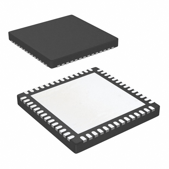
56-lead (8 mm × 8 mm) LFCSP package
Network synchronization, including synchronous Ethernet
and synchronous digital hierarchy (SDH) to optical
transport network (OTN) mapping/demapping
Cleanup of reference clock jitter
SONET/SDH clocks up to OC-192, including FEC
Stratum 3 holdover, jitter cleanup, and phase transient
control
Cable infrastructure
Data communications
Professional video
GENERAL DESCRIPTION
The AD9554-1 is a low loop bandwidth clock translator that
provides jitter cleanup and synchronization for many systems,
including synchronous optical networks (SONET/SDH). The
AD9554-1 generates an output clock synchronized to up to four
external input references. The digital PLLs (DPLLs) allow
reduction of input time jitter or phase noise associated with the
external references. The digitally controlled loop and holdover
circuitry of the AD9554-1 continuously generates a low jitter
output clock even when all reference inputs have failed.
The AD9554-1 operates over an industrial temperature range of
−40°C to +85°C. The AD9554 is a version of this device with
two outputs per PLL. If a single or dual DPLL version of this
device is needed, refer to the AD9557 or AD9559, respectively.
FUNCTIONAL BLOCK DIAGRAM
REFERENCE
INPUT
MONITOR
AND MUX
STABLE
SOURCE
SERIAL INTERFACE
(SPI OR I2C)
DIGITAL
PLL0
ANALOG
PLL0
÷3 TO ÷11
P0 DIVIDER
Q0_B DIVIDER
DIGITAL
PLL1
ANALOG
PLL1
÷3 TO ÷11
P1 DIVIDER
Q1_B DIVIDER
DIGITAL
PLL2
ANALOG
PLL2
÷3 TO ÷11
P2 DIVIDER
Q2_B DIVIDER
DIGITAL
PLL3
ANALOG
PLL3
÷3 TO ÷11
P3 DIVIDER
Q3_B DIVIDER
CLOCK
MULTIPLIER
AD9554-1
12214-001
STATUS AND
CONTROL PINS
Figure 1.
Rev. C
Document Feedback
Information furnished by Analog Devices is believed to be accurate and reliable. However, no
responsibility is assumed by Analog Devices for its use, nor for any infringements of patents or other
rights of third parties that may result from its use. Specifications subject to change without notice. No
license is granted by implication or otherwise under any patent or patent rights of Analog Devices.
Trademarks and registered trademarks are the property of their respective owners.
One Technology Way, P.O. Box 9106, Norwood, MA 02062-9106, U.S.A.
Tel: 781.329.4700 ©2014–2017 Analog Devices, Inc. All rights reserved.
Technical Support
www.analog.com
�AD9554-1
Data Sheet
TABLE OF CONTENTS
Features .............................................................................................. 1
Digital PLL (DPLL) Core .......................................................... 33
Applications ....................................................................................... 1
Loop Control State Machine ..................................................... 36
General Description ......................................................................... 1
System Clock (SYSCLK) ................................................................ 37
Functional Block Diagram .............................................................. 1
SYSCLK Inputs ........................................................................... 37
Revision History ............................................................................... 4
SYSCLK Multiplier ..................................................................... 37
Specifications..................................................................................... 5
Output Analog PLL (APLL) .......................................................... 39
Supply Voltage ............................................................................... 5
APLL Configuration .................................................................. 39
Supply Current .............................................................................. 5
APLL Calibration ....................................................................... 39
Power Dissipation ......................................................................... 6
Clock Distribution.......................................................................... 40
System Clock Inputs (XOA, XOB) ............................................. 6
Clock Dividers ............................................................................ 40
Reference Inputs ........................................................................... 7
Output Amplitude and Power-Down ...................................... 40
Reference Monitors ...................................................................... 8
Clock Distribution Synchronization........................................ 41
Reference Switchover Specifications .......................................... 8
Status and Control .......................................................................... 42
Distribution Clock Outputs ........................................................ 9
Multifunction Pins (M0 to M3 and M5 to M7) ......................... 42
Time Duration of Digital Functions ........................................ 11
IRQ Function .............................................................................. 42
Digital PLL (DPLL_0, DPLL_1, DPLL_2, and DPLL_3) ...... 11
Watchdog Timer ......................................................................... 43
Analog PLL (APLL_0, APLL_1, APLL_2, and APLL_3) ...... 11
Serial Control Port ......................................................................... 44
Digital PLL Lock Detection ...................................................... 12
SPI/I2C Port Selection................................................................ 44
Holdover Specifications ............................................................. 12
SPI Serial Port Operation .......................................................... 44
Serial Port Specifications—Serial Port Interface (SPI) Mode .... 12
I2C Serial Port Operation .......................................................... 47
Serial Port Specifications—I C Mode ...................................... 13
Programming the I/O Registers ................................................... 50
Logic Inputs (RESET, M0 to M3, M5 to M7) ......................... 14
Buffered/Active Registers .......................................................... 50
Logic Outputs (M0 to M3 and M5 to M7) .............................. 14
Write Detect Registers ............................................................... 50
Jitter Generation ......................................................................... 14
Autoclear Registers..................................................................... 50
Absolute Maximum Ratings.......................................................... 16
Register Access Restrictions...................................................... 50
ESD Caution ................................................................................ 16
Thermal Performance .................................................................... 51
Pin Configuration and Function Descriptions ........................... 17
Power Supply Partitions................................................................. 52
Typical Performance Characteristics ........................................... 20
VDD Supplies ............................................................................. 52
Input/Output Termination Recommendations .......................... 23
VDD_SP Supply ......................................................................... 52
Getting Started ................................................................................ 24
Register Map ................................................................................... 53
Chip Power Monitor and Startup ............................................. 24
Register Map Bit Descriptions ...................................................... 63
Multifunction Pins at Reset/Power-Up ................................... 24
Serial Control Port Configuration (Register 0x0000 to
Register 0x0001) ......................................................................... 63
2
Device Register Programming Using a Register Setup File ....... 24
Register Programming Overview ............................................. 28
Theory of Operation ...................................................................... 31
Overview...................................................................................... 31
Reference Input Physical Connections .................................... 32
Reference Monitors .................................................................... 32
Reference Input Block ................................................................ 32
Reference Switchover ................................................................. 33
Clock Part Family ID (Register 0x0003 to Register 0x0006) ..... 63
SPI Version (Register 0x000B).................................................. 64
Vendor ID (Register 0x000C to Register 0x000D) ................ 64
IO_Update (Register 0x000F) ................................................... 64
General Configuration (Register 0x0100 to Register 0x010E) .. 64
IRQ Mask (Register 0x010F to Register 0x011F) ................... 65
System Clock (Register 0x0200 to Register 0x0208) ............. 67
Rev. C | Page 2 of 99
�Data Sheet
AD9554-1
Reference Input A (Register 0x0300 to Register 0x031E) ......68
DPLL_3 Controls (Register 0x0700 to Register 0x071E) ........... 79
Reference Input B (Register 0x0320 to Register 0x033E) ......70
APLL_3 Configuration (Register 0x0730 to Register 0x0733) .. 79
Reference Input C (Register 0x0340 to Register 0x035E) ......70
PLL_3 Output Sync and Clock Distribution (Register 0x0734
to Register 0x073E) ..................................................................... 79
Reference Input D (Register 0x0360 to Register 0x037E) .....70
DPLL_0 Controls (Register 0x0400 to Register 0x041E).......70
APLL_0 Configuration (Register 0x0430 to Register 0x0434)...72
Output PLL_0 (APLL_0) Sync and Clock Distribution
(Register 0x0434 to Register 0x043E).......................................73
DPLL_0 Settings for Reference Input A (REFA)
(Register 0x0440 to Register 0x044C) ......................................74
DPLL_0 Settings for Reference Input B (REFB)
(Register 0x044D to Register 0x0459) ......................................75
DPLL_0 Settings for Reference Input C (REFC)
(Register 0x045A to Register 0x0466) ......................................76
DPLL_0 Settings for Reference Input D (REFD)
(Register 0x0467 to Register 0x0473) .......................................77
DPLL_1 Controls (Register 0x0500 to Register 0x051E).......78
DPLL_3 Settings for Reference Input A (REFA)
(Register 0x0740 to Register 0x074C) ...................................... 79
DPLL_3 Settings for Reference Input B (REFB)
(Register 0x074D to Register 0x0759) ...................................... 79
DPLL_3 Settings for Reference Input C (REFC)
(Register 0x075A to Register 0x0766) ...................................... 80
DPLL_3 Settings for Reference Input D (REFD)
(Register 0x0767 to Register 0x0773) ....................................... 80
Digital Loop Filter Coefficients (Register 0x0800 to
Register 0x0817) .......................................................................... 80
Common Operational Controls (Register 0x0A00 to
Register 0x0A0E) ........................................................................ 81
IRQ Clearing (Register 0x0A05 to Register 0x0A14) ............ 83
APLL_1 Configuration (Register 0x0530 to Register 0x0533)...78
PLL_0 Operational Controls (Register 0x0A20 to
Register 0x0A24) ......................................................................... 86
PLL_1 Output Sync and Clock Distribution (Register 0x0534
to Register 0x053E) .....................................................................78
PLL_1 Operational Controls (Register 0x0A40 to
Register 0x0A44) ......................................................................... 88
DPLL_1 Settings for Reference Input A (REFA)
(Register 0x0540 to Register 0x054C) ......................................78
PLL_2 Operational Controls (Register 0x0A60 to
Register 0x0A64) ......................................................................... 88
DPLL_1 Settings for Reference Input B (REFB)
(Register 0x054D to Register 0x0559) ......................................78
PLL_3 Operational Controls (Register 0x0A80 to
Register 0x0A84) ......................................................................... 88
DPLL_1 Settings for Reference Input C (REFC)
(Register 0x055A to Register 0x0566) ......................................79
Voltage Regulator (Register 0x0B00 to Register 0x0B01)...... 88
DPLL_1 Settings for Reference Input D (REFD)
(Register 0x0567 to Register 0x0573) .......................................79
IRQ Monitor (Register 0x0D08 to Register 0x0D16) ............ 90
DPLL_2 Controls (Register 0x0600 to Register 0x061E).......79
APLL_2 Configuration (Register 0x0630 to Register 0x0633)...79
PLL_2 Output Sync and Clock Distribution (Register 0x0634
to Register 0x063E) .....................................................................79
DPLL_2 Settings for Reference Input A (REFA)
(Register 0x0640 to Register 0x064C) ......................................79
DPLL_2 Settings for Reference Input B (REFB)
(Register 0x064D to Register 0x0659) ......................................79
DPLL_2 Settings for Reference Input C (REFC)
(Register 0x065A to Register 0x0666) ......................................79
Status Readback (Register 0x0D01 to Register 0x0D05) ....... 88
PLL_0 Read Only Status (Register 0x0D20 to
Register 0x0D2A) ........................................................................ 93
PLL_1 Read Only Status (Register 0x0D40 to
Register 0x0D4A) ........................................................................ 95
PLL_2 Read Only Status (Register 0x0D60 to
Register 0x0D6A) ........................................................................ 95
PLL_3 Read Only Status (Register 0x0D80 to
Register 0x0D8A) ........................................................................ 95
Outline Dimensions ........................................................................ 99
Ordering Guide ........................................................................... 99
DPLL_2 Settings for Reference Input D (REFD)
(Register 0x0667 to Register 0x0673) .......................................79
Rev. C | Page 3 of 99
�AD9554-1
Data Sheet
REVISION HISTORY
3/2017—Rev. B to Rev. C
Changes to Chip Power and Startup Section .............................. 24
Changes to Figure 25 ...................................................................... 25
Changes to Outline Dimensions................................................... 99
Changes to Ordering Guide .......................................................... 99
10/2016—Rev. A to Rev. B
Changes to Figure 2 ........................................................................ 17
Deleted Figure 3; Renumbered Sequentially............................... 20
Changes to Device Register Programming Using a Register
Setup File Section ........................................................................... 24
Added Figure 26; Renumbered Sequentially .............................. 25
Added Figure 27.............................................................................. 26
Added Figure 28.............................................................................. 27
Added Figure 29.............................................................................. 28
Changes to Register Programming Overview Section .............. 28
Changes to DPLL Feedback Dividers Section ............................ 30
Changes to DPLL Phase Lock Detector Section ........................ 35
Change to APLL Calibration Section........................................... 39
Changes to Table 62 ........................................................................ 73
Added Endnote 1, Table 67 ........................................................... 75
Changes to Table 73, Table 75, and Table 76 ............................... 77
Changes to Table 77, Table 78, Table 79, and Table 80 .............. 78
Changes to Table 82, Table 83, Table 84, Table 85,
and Table 86 ..................................................................................... 79
Changes to Table 87, Table 88, Table 89, and Table 90 .............. 80
Changes to Table 91 and Table 92 ................................................ 82
Changes to Table 94 ........................................................................ 83
Changes to Table 122...................................................................... 96
8/2014—Rev. 0 to Rev. A
Added Bandwidth (fREF = 19.44 MHz; fOUT = 156.25 MHz;
fLOOP = 50 Hz) Parameters; Table 18 ............................................. 15
Changes to Figure 3 ........................................................................ 20
Changes to Figure 27...................................................................... 31
Changes to APLL Calibration Section ......................................... 36
Changes to Output Amplitude and Power-Down Section ....... 37
Changes to Table 69 ....................................................................... 71
4/2014—Revision 0: Initial Version
Rev. C | Page 4 of 99
�Data Sheet
AD9554-1
SPECIFICATIONS
Minimum (min) and maximum (max) values apply for the full range of supply voltage and operating temperature variations. Typical (typ)
values apply for VDD = 1.8 V, TA = 25°C, unless otherwise noted.
SUPPLY VOLTAGE
Table 1.
Parameter
SUPPLY VOLTAGE FOR 1.8 V OPERATION
VDD_SP
VDD
SUPPLY VOLTAGE FOR 1.5 V OPERATION
VDD_SP
VDD
Min
Typ
Max
Unit
1.47
1.71
1.8
1.8
2.625
1.89
V
V
1.47
1.47
1.5
1.5
2.625
1.53
V
V
SUPPLY CURRENT
The test conditions for the maximum (max) supply current are at the maximum supply voltage found in Table 1. The test conditions for
the typical (typ) supply current are at the typical supply voltage found in Table 1. The test conditions for the minimum (min) supply
current are at the minimum supply voltage found in Table 1.
Table 2.
Parameter
SUPPLY CURRENT FOR TYPICAL CONFIGURATION
Min
Typ
Max
Unit
IVDD_SP
IVDD
SUPPLY CURRENT FOR ALL BLOCKS RUNNING CONFIGURATION
0.01
450
0.04
513
0.1
560
mA
mA
IVDD_SP
IVDD
Test Conditions/Comments
Typical values are for the Typical
Configuration parameter
listed in Table 3; valid for both 1.5 V and 1.8 V
operation
Maximum values are for the All Blocks
Running parameter
listed in Table 3; valid for both 1.5 V and 1.8 V
operation
0.01
450
0.04
566
Rev. C | Page 5 of 99
0.1
650
mA
mA
�AD9554-1
Data Sheet
POWER DISSIPATION
Typical (typ) values apply for VDD = 1.8 V and maximum (max) values for VDD = 1.89 V.
Table 3.
Parameter
POWER DISSIPATION
Typical Configuration
Min
Typ
Max
Unit
Test Conditions/Comments
0.92
1.1
W
All Blocks Running
1.02
1.2
W
Full Power-Down
164
mW
190
mW
System clock: 49.152 MHz crystal; four DPLLs active;
two 19.44 MHz input references in differential mode;
four ac-coupled output drivers in 21 mA mode at
644.53125 MHz
System clock: 49.152 MHz crystal; four DPLLs active,
four 19.44 MHz input references in differential mode;
eight ac-coupled output drivers in 28 mA mode at
750 MHz
Measured using the Typical Configuration parameter
(see Table 3) and then setting the full power down bit
Typical configuration; table values show the change in
power due to the indicated operation
Power delta computed relative to the typical
configuration; the blocks powered down include one
reference input, one DPLL, one APLL, one P divider, two
channel dividers, two output drivers in 28 mA mode
22.5
24.6
14.3
mW
mW
mW
70
48
23.6
mW
mW
mW
Incremental Power Dissipation
Complete DPLL/APLL On/Off
Input Reference On/Off
Differential (Normal Mode)
Differential (DC-Coupled LVDS)
Single-Ended
Output Distribution Driver On/Off
28 mA Mode (at 644.53 MHz)
21 mA Mode (at 644.53 MHz)
14 mA mode (at 644.53 MHz)
fREF = 19.44 MHz
fREF = 19.44 MHz
fREF = 19.44 MHz
SYSTEM CLOCK INPUTS (XOA, XOB)
Table 4.
Parameter
SYSTEM CLOCK MULTIPLIER
PLL Output Frequency Range
Min
Phase Frequency Detector (PFD) Rate
Frequency Multiplication Range
SYSTEM CLOCK REFERENCE INPUT PATH
Input Frequency Range
System Clock Input Doubler Disabled
System Clock Input Doubler Enabled
Minimum Input Slew Rate
Self-Biased Common-Mode Voltage
Input High Voltage
Input Low Voltage
Differential Input Voltage Sensitivity
Typ
Max
Unit
Test Conditions/Comments
2250
2415
MHz
Voltage controlled oscillator (VCO) range can place
limitations on nonstandard system clock input frequencies
10
8
300
241
MHz
10
16
250
268
150
MHz
MHz
V/μs
V
V
V
mV p-p
0.72
0.9
0.5
250
Assumes valid system clock and PFD rates
System clock input must be ac-coupled
Rev. C | Page 6 of 99
Minimum limit imposed for jitter performance
Internally generated
For ac-coupled single-ended operation
For ac-coupled single-ended operation
Minimum voltage across pins required to ensure switching
between logic states; the instantaneous voltage on either
pin must not exceed 1.14 V; single-ended input can be
accommodated by ac grounding complementary input;
800 mV p-p recommended for optimal jitter performance
�Data Sheet
AD9554-1
Parameter
System Clock Input Doubler Duty Cycle
Min
Typ
Max
Unit
System Clock Input = 20 MHz to 150 MHz
System Clock Input = 16 MHz to 20 MHz
Input Capacitance
Input Resistance
CRYSTAL RESONATOR PATH
Crystal Resonator Frequency Range
Input Capacitance
Maximum Crystal Motional Resistance
43
47
50
50
3
5
57
53
%
%
pF
kΩ
12
50
3
100
MHz
pF
Ω
Test Conditions/Comments
Amount of duty-cycle variation that can be tolerated on
the system clock input to use the doubler
Single-ended to ground, each pin
Fundamental mode, AT cut crystal
Single-ended to ground, each pin
REFERENCE INPUTS
Table 5.
Parameter
DIFFERENTIAL MODE
Frequency Range
Sinusoidal Input
LVPECL Input
LVDS Input
Minimum Input Slew Rate
DPLL Loop Bandwidth = 50 Hz
DPLL Loop Bandwidth = 4 kHz
Common-Mode Input Voltage
Differential Input Voltage Sensitivity
fIN < 400 MHz
fIN = 400 MHz to 750 MHz
fIN = 750 MHz to 1000 MHz
Differential Input Voltage Hysteresis
Input Resistance
Input Capacitance
Minimum Pulse Width High
LVPECL
LVDS
Minimum Pulse Width Low
LVPECL
LVDS
DC-COUPLED LVDS MODE
Frequency Range
Minimum Input Slew Rate
DPLL Loop Bandwidth = 50 Hz
DPLL Loop Bandwidth = 4 kHz
Common-Mode Input Voltage
Differential Input Voltage Sensitivity
Differential Input Voltage Hysteresis
Input Resistance
Input Capacitance
Minimum Pulse Width High
Minimum Pulse Width Low
Min
Typ
10
0.002
0.002
Max
Unit
475
1000
700
MHz
MHz
MHz
40
50
V/μs
V/μs
V
0.64
400
500
1000
55
16
9
2100
2100
2100
100
mV p-p
mV p-p
mV p-p
mV
kΩ
pF
460
560
ps
ps
460
560
ps
ps
Test Conditions/Comments
AC couple inputs in differential mode
Assumes an LVDS minimum of 494 mV p-p differential
amplitude
Minimum limit imposed for jitter performance
Maximum loop bandwidth is fPFD/50
Internally generated self-bias voltage
Peak-to-peak differential voltage swing across pins
required to ensure switching between logic levels as
measured with a differential probe; instantaneous voltage
on either pin must not exceed 1.3 V
Equivalent differential input resistance
Single-ended to ground, each pin
Intended for dc-coupled LVDS ≤ 10.24 MHz
0.002
10.24
MHz
1.375
1200
V/μs
V/μs
V
mV
Minimum limit imposed for jitter performance
40
150
1.125
400
55
21
7
25
25
100
mV
kΩ
pF
ns
ns
Rev. C | Page 7 of 99
Maximum loop bandwidth is fPFD/50
Differential voltage across pins required to ensure
switching between logic levels; instantaneous voltage on
either pin must not exceed the supply rails
�AD9554-1
Data Sheet
Parameter
SINGLE-ENDED MODE
Frequency Range (CMOS)
Minimum Input Slew Rate
DPLL Loop Bandwidth = 50 Hz
DPLL Loop Bandwidth = 4 kHz
Input Voltage High, VIH
Input Voltage Low, VIL
Input Resistance
Input Capacitance
Minimum Pulse Width High
Minimum Pulse Width Low
Min
Typ
0.002
Max
Unit
300
MHz
Test Conditions/Comments
DC-coupled
Minimum limit imposed for jitter performance
40
175
VDD − 0.5
V/μs
V/μs
V
V
kΩ
pF
ns
ns
0.5
30
5
1.5
1.5
Maximum loop bandwidth is fPFD/50
REFERENCE MONITORS
Table 6.
Parameter
REFERENCE MONITORS
Reference Monitor
Loss of Reference Detection Time
Frequency Out-of Range Limits
Validation Timer
Min
Typ
Max
Unit
Test Conditions/Comments
1.15
DPLL PFD period
2
105
Δf/fREF (ppm)
0.001
65.535
sec
Nominal phase detector period = R/fREF, where R is the
frequency division factor determined by the R divider,
and fREF is the frequency of the active reference
Programmable (lower bound subject to quality of the
system clock [SYSCLK]); SYSCLK accuracy must be less
than the lower bound
Programmable in 1 ms increments
REFERENCE SWITCHOVER SPECIFICATIONS
Table 7.
Parameter
MAXIMUM OUTPUT PHASE PERTURBATION
(PHASE BUILD-OUT SWITCHOVER)
Min
Typ
Max
Unit
±20
±20
±130
±130
ps
ps
10
DPLL
PFD
period
50 Hz DPLL Loop Bandwidth
Peak
Steady State
Time Required to Switch to a New Reference
Phase Build-Out Switchover
Rev. C | Page 8 of 99
Test Conditions/Comments
Assumes a jitter-free reference; satisfies
Telcordia GR-1244-CORE requirements; base
loop filter selection bit set to 1b or all active
references
High phase margin mode; 19.44 MHz to
174.70308 MHz; DPLL bandwidth = 50 Hz;
49.152 MHz signal generator used for system
clock source
Calculated using the nominal phase detector
period (NPDP = R/fREF); the total time required
is the time plus the reference validation time,
plus the time required to lock to the new
reference
�Data Sheet
AD9554-1
DISTRIBUTION CLOCK OUTPUTS
Table 8.
Parameter
14 mA (HCSL-, LVDS-COMPATIBLE) MODE
Min
Typ
Max
Unit
Output Frequency
0.430
941
MHz
Continuous Output Frequency Range
0.430
781
MHz
Maximum Output Frequency
PLL0 to PLL3 Using Unique VCO
Frequencies
PLL0, PLL1, and PLL2
PLL3
Rise/Fall Time (20% to 80%)1
Duty Cycle
Up to fOUT = 750 MHz
Up to fOUT = 941 MHz
Up to fOUT = 1250 MHz
Differential Output Voltage Swing
Without 100 Ω Termination Resistor
With 100 Ω Termination Resistor Across
Outputs
Common-Mode Output Voltage
Reference Input-to-Output Delay Variation
over Temperature
Static Phase Offset Variation from Active
Reference to Output over Voltage Extremes
21 mA MODE
941
MHz
1250
MHz
1187
125
45
44
50
50
50
190
55
56
MHz
ps
Differential voltage swing between output
pins; measured with output driver static; peakto-peak differential output amplitude 2× this
level with driver toggling; see Figure 10 for
output amplitude vs. output frequency
635
294
840
390
1000
463
mV
mV
310
420
600
525
mV
fs/°C
±75
Output driver static; no termination resistor
DPLL locked to same input reference at all
times; stable system clock source (noncrystal)
fs/mV
0.430
941
MHz
Continuous Output Frequency Range
0.430
781
MHz
PLL3
Maximum frequency all four PLLs can
generate using unique VCO frequencies
Limited by 1250 MHz maximum input
frequency to channel divider (Q divider)
Limited by 4748 MHz maximum VCO frequency
%
%
%
Output Frequency
Maximum Output Frequency
PLL0 to PLL3 Using Unique VCO
Frequencies
PLL0, PLL1, and PLL2
Test Conditions/Comments
Unless otherwise stated, specifications dccoupled with no output termination resistor;
when ac-coupled, LVDS-compatible amplitudes
are achieved with a 100 Ω resistor across the
output pair; HCSL-compatible amplitudes
achieved with no termination resistor across
the output pair; output current setting: 14 mA
Frequency range all four PLLs can generate using
unique VCO frequencies; frequencies outside
this range are possible on some of the PLLs, but
can result in increased VCO coupling due to
multiple PLLs using the same VCO frequency
All four PLLs can generate this range at the
same time while using unique VCO frequencies
941
MHz
1250
MHz
1187
MHz
Rev. C | Page 9 of 99
Unless otherwise stated, specifications
dc-coupled with 50 Ω output termination resistor
to ground; output current setting = 21 mA
Frequency range all four PLLs can generate using
unique VCO frequencies; frequencies outside
this range are possible on some of the PLLs, but
can result in increased VCO coupling due to
multiple PLLs using the same VCO frequency
All four PLLs can generate this range at the
same time while using unique VCO frequencies
Maximum frequency all four PLLs can
generate using unique VCO frequencies
Limited by 1250 MHz maximum input
frequency to channel divider (Q divider)
Limited by 4748 MHz maximum VCO frequency
�AD9554-1
Parameter
Rise/Fall Time (20% to 80%)1
Duty Cycle
Up to fOUT = 750 MHz
Up to fOUT = 941 MHz
Up to fOUT = 1250 MHz
Differential Output Voltage Swing
No External Termination Resistor
With 50 Ω Termination Resistor to
Ground on Each Leg
Common-Mode Output Voltage
Data Sheet
Min
Typ
125
Max
190
Unit
ps
45
44
50
50
50
55
56
%
%
%
Differential voltage swing between output
pins; measured with output driver static; peakto-peak differential output amplitude 2× this
level with driver toggling; see Figure 12 for
output amplitude vs. output frequency
779
413
1180
625
1510
800
mV
mV
206
312
400
mV
Reference Input-to-Output Delay Variation
over Temperature
Static Phase Offset Variation from Active
Reference to Output over Voltage Extremes
28 mA (LVPECL-COMPATIBLE) MODE
fs/°C
±75
fs/mV
0.430
941
MHz
Continuous Output Frequency Range
0.430
781
MHz
Maximum Output Frequency
PLL0 to PLL3 Using Unique VCO
Frequencies
PLL0, PLL1, and PLL2
Common-Mode Output Voltage
941
MHz
1250
MHz
1187
185
45
44
280
55
56
MHz
ps
540
50
50
50
830
1020
%
%
%
mV
275
415
510
mV
Reference Input-to-Output Delay Variation
over Temperature
Static Phase Offset Variation from Active
Reference to Output over Voltage Extremes
1
600
Output Frequency
PLL3
Rise/Fall Time (20% to 80%)1
Duty Cycle
Up to fOUT = 750 MHz
Up to fOUT = 941 MHz
Up to fOUT = 1250 MHz
Differential Output Voltage Swing
Test Conditions/Comments
600
fs/°C
±75
fs/mV
The listed values are for the slower edge (rising or falling).
Rev. C | Page 10 of 99
Output driver static with 50 Ω resistor to
ground on each leg
DPLL locked to same input reference at all
times; stable system clock source (noncrystal)
Specifications for dc-coupled, 50 Ω termination
resistor from each leg to ground; ac coupling
used in most applications; output current
setting = 28 mA; in this mode, user must have
either a 50 Ω resistor from each leg to ground,
or a 100 Ω resistor across the differential pair
Frequency range all four PLLs can generate using
unique VCO frequencies; frequencies outside
this range are possible on some of the PLLs, but
can result in increased VCO coupling due to
multiple PLLs using the same VCO frequency
Frequency range for each PLL such that all four
PLLs are using unique VCO frequencies with
no frequency gaps
Maximum frequency all four PLLs can
generate using unique VCO frequencies
Limited by 1250 MHz maximum input
frequency to channel divider (Q divider)
Limited by 4748 MHz maximum VCO frequency
Differential voltage swing between output
pins; measured with output driver static; peakto-peak differential output amplitude 2× this
level with driver toggling; see Figure 9 for
output amplitude vs. output frequency
Output driver static; 50 Ω external termination
resistor from each leg to ground
DPLL locked to same input reference at all
times; stable system clock source (noncrystal)
�Data Sheet
AD9554-1
TIME DURATION OF DIGITAL FUNCTIONS
Table 9.
Parameter
TIME DURATION OF DIGITAL FUNCTIONS
Power-Down Exit Time
Min
Typ
Max
51
1
1
10
Mx Pin to RESET Rising Edge Setup Time
Mx Pin to RESET Rising Edge Hold Time
RESET Falling Edge to Mx Pin High-Z Time
Unit
Test Conditions/Comments
ms
Time from power-down exit to system clock stable (including
the system clock stability timer default of 50 ms); does not
include time to validate input references or lock the DPLL
Mx refers to the M0, M1, M2, M3, M5, M6, M7 pins
ns
ns
ns
DIGITAL PLL (DPLL_0, DPLL_1, DPLL_2, AND DPLL_3)
Table 10.
Parameter
DIGITAL PLL
Phase Frequency Detector (PFD)
Input Frequency Range
Loop Bandwidth
Phase Margin
Closed Loop Peaking
Min
Typ
Max
Unit
2
200
kHz
0.1
45
SYSCLK_TO*
YES
YES
*SYSCLK_TO IS A CALCULATED TIMEOUT VALUE. IT IS 100ms AND SYSTEM CLOCK VALIDATION
TIME (REGISTER 0x206 TO REGISTER 0x208: DEFAULT = 50ms)
Figure 26. Subprocess—System Clock Initialization
Rev. C | Page 26 of 99
12214-101
END
�Data Sheet
AD9554-1
START
APLL RECALIBRATION LOOP1
CAL_COUNT = 0
VCO
CALIBRATION
OPERATION
WRITE:
CAL REG BIT 1 = 0
APLL
ALL
0
1
2
3
CAL REG
0xA00
0xA20
0xA40
0xA60
0xA80
LOCK REG
0xD00 2
0xD20
0xD40
0xD60
0xD80
SYNC REG
0xA00
0xA20
0xA40
0xA60
0xA80
NO
WRITE:
REGISTER 0x00F = 0x01
CAL_COUNT > 1
YES
END
(TO RST_COUNT CHECK)
WRITE:
CAL REG BIT 1 = 1
WRITE:
REGISTER 0x00F = 0x01
CAL_COUNT =
CAL_COUNT + 1
START TIMEOUT CLOCK:
TIME = 0
APLL LOCK
DETECT POLLING
LOOP
NO
LOCK REG BIT 3 = 1
NO
TIMEOUT CLOCK:
TIME > 200ms
YES
YES
ENSURE THAT CAL REG BIT 1 = 0
FOR ALL CALIBRATION REGISTERS
(0xA00, 0xA20, 0xA40, 0xA60, 0xA80)
WRITE:
SYNC REG BIT 2 = 1
DISTRIBUTION
SYNCHRONIZATION
OPERATION
WRITE:
REGISTER 0x00F = 0x01
WRITE:
SYNC REG BIT 2 = 0
WRITE:
REGISTER 0x00F = 0x01
END
THAT THE CALIBRATE ALL AND SOFT SYNC ALL BITS IN REGISTER 0x0A00 CAN BE USED IF THE USER
WANTS TO CALIBRATE OR SYNC ALL FOUR PLLs SIMULTANEOUSLY INSTEAD OF ONE AT A TIME.
HOWEVER, THE USER MUST STILL VERIFY THAT ALL FOUR APLLs ARE LOCKED BY READING THE
INDIVIDUAL APLL LOCK REGISTERS.
2REGISTER 0x0D00 CAN ONLY BE USED TO VERIFY THE LOCK STATE OF EACH APLL
IF THE CORRESPONDING DPLL IS ALSO LOCKED.
Figure 27. Subprocess—Analog PLL Initialization
Rev. C | Page 27 of 99
12214-102
1NOTE
�AD9554-1
Data Sheet
START
DISTRIBUTION
SYNCHRONIZATION:
DISABLE OUTxA/OUTxB
TOGGLING
WRITE:
SYNC REG BIT 2 = 1
CHANNEL
0
1
2
3
WRITE:
REGISTER 0x00F = 0x01
SYNC REG
0xA20
0xA40
0xA60
0xA80
SOFTWARE GENERATED
AD9554-1 RELATED
REGISTERS FOR DIFFERENT
DPLL CONFIGURATIONS
WRITE NEW
BUSINESS CASE
RELATED REGISTERS
WRITE:
REGISTER 0x00F = 0x01
OUTPUT CLOCK
DISTRIBUTION
SYNCHRONIZATION
FOR PLL_x
12214-103
SUBPROCESS:
ANALOG PLL_x
INITIALIZATION
END
Figure 28. Main Process—PLL Reconfiguration
REGISTER PROGRAMMING OVERVIEW
This section provides a programming overview of the register
blocks in the AD9554-1, describing each function and why they
are important. This is supplemental information only needed
when loading the registers without using the .STP file.
The AD9554-1 evaluation software contains a wizard that
determines the register settings based on the input and output
frequencies of the user. It is strongly recommended that the
evaluation software be used to determine these settings.
Multifunction Pins (Optional)
To use any of the multifunction pins for status or control, this
step is required. The multifunction pin parameters are located
at Register 0x0100 to Register 0x010A.
Table 123 has a list of the Mx pin output functions, and Table 124
has a list of Mx pin input functions.
IRQ Functions (Optional)
To use the IRQ feature, this step is required. The IRQ functions
are divided into five groups: common, PLL_0, PLL_1, PLL_2,
and PLL_3.
First, choose the events that trigger an IRQ and then set them in
Register 0x010F to Register 0x011D. Next, an Mx pin must be
assigned to the IRQ function. The user can choose to dedicate
one Mx pin to each of the five IRQ groups, or one Mx pin can
be assigned for all IRQs.
Individual IRQ events are cleared by using the IRQ clearing
registers at Register 0x0A05 to Register 0x0A14 or by setting the
clear all IRQs bit (Register 0x0A05[0]) to 1b.
The default values of the IRQ mask registers are such that
interrupts are not generated. The default IRQ pin (and Mx pins)
mode is active high CMOS. The user can also select active low
CMOS, open-drain PMOS, and open-drain NMOS independently
on any of these pins.
Watchdog Timer (Optional)
To use the watchdog timer, this step is required. The watchdog
timer control is located at Register 0x010D and Register 0x010E.
The watchdog timer is disabled by default.
The watchdog timer is useful for generating an IRQ at a fixed
interval. The timer is reset by setting the clear watchdog timer
bit in Register 0x0A05[7] to 1.
The user can also program an Mx pin for the watchdog timer
output. In this mode, the Mx pin generates a 40 ns pulse every
time the watchdog timer expires.
System Clock Configuration
The system clock multiplier (SYSCLK) parameters are at
Register 0x0200 to Register 0x0208. For optimal performance,
use the following steps:
1.
2.
The IRQ monitor registers are located at Register 0x0D08 to
Register 0x0D16. If the desired bits in the IRQ mask registers at
Register 0x010F to Register 0x011D are set high, the appropriate
IRQ monitor bit at Register 0x0D08 to Register 0x0D16 is set
high when the indicated event occurs.
Rev. C | Page 28 of 99
Set the system clock PLL input type and divider values.
Set the system clock period. It is essential to program the
system clock period because many of the AD9554-1
subsystems rely on this value.
�Data Sheet
3.
4.
5.
6.
AD9554-1
Set the system clock stability timer. The system clock stability
timer specifies the amount of time that the system clock
PLL must be locked before the device declares that the system
clock is stable. It is critical that the system clock stability
timer be set long enough to ensure that the external source is
completely stable when the timer expires. For instance, a
temperature compensated crystal oscillator (TCXO) can
take longer than 50 ms (the default value for the stability
timer) to stabilize after power is applied.
Update all registers (Register 0x000F = 0x01).
To calibrate the system clock on the next IO_UPDATE,
write Register 0x0A00 = 0x04.
Update all registers (Register 0x000F = 0x01).
Important Notes
If Bit 2 in Register 0x0A00 is set independently to initiate a
system clock PLL calibration, leave this bit set to 1 in all
subsequent writes to Register 0x0A00. If this bit is accidentally
cleared, recalibrate the system clock VCO or issue a calibrate all
command by setting Bit 1 in Register 0x0A00 and by issuing an
IO_UPDATE (Register 0x000F = 0x01).
In addition, the system clock PLL must be locked for the digital
PLL blocks to function correctly and to read back the registers
updated on the system clock domain. These registers include
the status registers, as well as the free running tuning word.
APLL calibration and input reference monitoring and validation
require that the system clock be stable. Therefore, first ensure that
the system clock is stable by checking Bit 1 in Register 0x0D01
when debugging the AD9554-1.
Reference switching mode settings are found in
Register 0x0A22 (DPLL_0), Register 0x0A42 (DPLL_1),
Register 0x0A62 (DPLL_2), and Register 0x0A82 (DPLL_3).
Digital PLL (DPLL) Controls and Settings
The DPLL control parameters are separate for DPLL_0 through
DPLL_3. They reside in the following registers:
Register 0x0400 to Register 0x041E (DPLL_0)
Register 0x0500 to Register 0x051E (DPLL_1)
Register 0x0600 to Register 0x061E (DPLL_2)
Register 0x0700 to Register 0x071E (DPLL_3)
These registers include the following settings:
30-bit free running frequency
DPLL pull-in range limits
DPLL closed-loop phase offset
Tuning word history control (for holdover operation)
Phase slew control (for controlling the phase slew rate
during a closed-loop phase adjustment)
Demapping control
With the exception of the free running tuning word, the default
values of these registers are fine for normal operation. The free
running frequency of the DPLL determines the frequency that
appears at the APLL input when user free run mode is selected.
The correct free running frequency is required for the APLL to
calibrate and lock correctly.
Output PLLs (APLLs) and Output Drivers
Reference Inputs
The registers that control the APLLs and output drivers reside
in the following registers:
The reference input parameters and reference dividers are common
to all PLLs; there is only one reference divider (R divider) for
each reference input. The register address for each reference
input follows:
Register 0x0300 to Register 0x031E for REFA
Register 0x0320 to Register 0x033E for REFB
Register 0x0340 to Register 0x035E for REFC
Register 0x0360 to Register 0x037E for REFD
The following functions are controlled in these registers:
These registers include the following settings:
Reference logic type (such as differential, single-ended)
Reference divider (20-bit R divider value)
Reference input period and tolerance
Reference validation timer
Phase and frequency lock detector settings
Phase step threshold
APLL settings (feedback divider, charge pump current)
Output synchronization mode
Output divider values
Output enable/disable (disabled by default)
Output logic type
The APLL calibration and synchronization bits reside in the
following registers:
Other reference input settings are in the following registers:
Register 0x0430 to Register 0x043E (APLL_0)
Register 0x0530 to Register 0x053E (APLL_1)
Register 0x0630 to Register 0x063E (APLL_2)
Register 0x0730 to Register 0x073E (APLL_3)
Reference input enable information is found in the DPLL
Feedback Dividers section.
Reference power-down information is found in
Register 0x0A01.
Rev. C | Page 29 of 99
Register 0x0A20 (APLL_0)
Register 0x0A40 (APLL_1)
Register 0x0A60 (APLL_2)
Register 0x0A80 (APLL_3)
�AD9554-1
Data Sheet
DPLL Feedback Dividers
APLL VCO Calibration
Each DPLL has separate feedback divider settings for each
reference input, which allows the user to have each digital PLL
perform a different frequency translation. However, there is
only one reference divider (R divider) for each reference input.
VCO calibration ensures that the VCO has sufficient operating
margin to function across the full temperature range. The user
can calibrate each of the four VCOs independently of one
another. When calibrating the APLL VCO, it is important to
remember the following conditions:
The feedback divider register settings for DPLL_0 reside in the
following registers. Feedback divider registers for the remaining
three DPLLs mimic the structure of the DPLL_0 registers, but
are offset by 0x0100 registers.
Register 0x0440 to Register 0x44C (DPLL_0 for REFA)
Register 0x044D to Register 0x459 (DPLL_0 for REFB)
Register 0x045A to Register 0x466 (DPLL_0 for REFC)
Register 0x0467 to Register 0x473 (DPLL_0 for REFD)
DPLL_1 for REFA to DPLL_1 for REFD: Same as DPLL_0
but register addresses offset by 0x0100
DPLL_2 for REFA to DPLL_2 for REFD: Same as DPLL_0
but register addresses offset by 0x0200
DPLL_3 for REFA to DPLL_3 for REFD: Same as DPLL_0
but register addresses offset by 0x0300
These registers include the following settings:
Reference priority
Reference input enable (separate for each DPLL)
DPLL loop bandwidth and loop filter selection
DPLL feedback divider (integer portion)
DPLL feedback divider (fractional portion)
DPLL feedback divider (modulus portion)
Common Operational Controls
The common operational controls reside at Register 0x0A00 to
Register 0x0A14 and include the following:
Simultaneous calibration and synchronization of all PLLs
Global power-down
Reference power-down
Reference validation override
IRQ clearing (for all IRQs)
PLL_0 Through PLL_3 Operational Controls
The PLL_0 through PLL_3 operational controls are located at
Register 0x0A20 to Register 0x0A84 and include the following:
APLL calibration and synchronization
Output driver enable and power-down
DPLL reference input switching modes
DPLL open-loop phase stepping control
Generate the Output Clock
If Register 0x0435 (for PLL_0), Register 0x0535 (for PLL_1),
Register 0x0635 (for PLL_2), or Register 0x0735 (for PLL_3) is
programmed for automatic clock distribution synchronization
via the DPLL phase or frequency lock, the synthesized output
signal appears at the clock distribution outputs. Otherwise, set and
then clear the soft sync bit (Bit 2 in Register 0x0A20 for APLL_0,
Bit 2 in Register 0x0A40 for APLL_1, Bit 2 in Register 0x0A60
for APLL_2, and Bit 2 in Register 0x0A80 for APLL_3) or use a
multifunction pin input (if programmed accordingly) to generate a
clock distribution sync pulse. This sync pulse causes the
synthesized output signal to appear at the clock distribution
outputs. Note that the sync pulse is delayed until the APLL
achieves lock following APLL calibration.
Generate the Reference Acquisition
The user free run bits that enable user free run mode reside in
the following registers:
The APLL VCO calibration does not occur until the system
clock is stable.
The APLL VCO must have the correct frequency from the
30-bit digitally controlled oscillator (DCO) during
calibration. The free running tuning word is found in
Register 0x0400 to Register 0x0403 (DPLL_0),
Register 0x0500 to Register 0x0503 (DPLL_1),
Register 0x0600 to Register 0x0603 (DPLL_2), and
Register 0x0700 to Register 0x0703 (DPLL_3).
The APLL VCO must be recalibrated any time the APLL
frequency changes.
APLL VCO calibration occurs on the low to high transition
of the APLL VCO calibration bit (Register 0x0A20[1] for
APLL_0, Register 0x0A40[1] for APLL_1, Register 0x0A60[1]
for APLL_2, and Register 0x0A80[1] for APLL_3).
The VCO calibration bit is not an autoclearing bit.
Therefore, this bit must be cleared (and an IO_UPDATE
issued) before the APLL is recalibrated.
The best way to monitor successful APLL calibration is by
monitoring the APLL locked bit in the following registers:
Register 0x0D20[3] for APLL_0, Register 0x0D40[3] for
APLL_1, Register 0x0D60[3] for APLL_2, and
Register 0x0D80[3] for APLL_3.
After the registers are programmed, the DPLLs lock to the
reference input that has been manually selected (if any), or the
first available reference that has the highest priority.
Register 0x0A22 = 0x01 (DPLL_0)
Register 0x0A42 = 0x01 (DPLL_1)
Register 0x0A62 = 0x01 (DPLL_2)
Register 0x0A82 = 0x01 (DPLL_3)
Rev. C | Page 30 of 99
�Data Sheet
AD9554-1
THEORY OF OPERATION
XOB
REF
OR
XTAL
SYSCLK
MULTIPLIER
×2
÷2, ÷4, ÷8
LOOP
FILTER
SYSTEM
CLOCK
INPUT REFERENCE
FREQUENCY RANGE:
2kHz TO 1000MHz
REFA
REFA
A
÷RA
REFB
REFB
B
÷RB
REFC
REFC
C
÷RC
REFD
REFD
D
÷RD
DPFD
REFERENCE
MONITORS
AND
CROSSPOINT
MUX
TW
CLAMP
÷N0
÷Q0_B
LF
÷M0
VCO_0
CONTROL
INTERFACE/LOGIC
SDIO/SDA
CS
OUT1B
OUT1B
SAME DETAIL AS PLL0
VCO_2 RANGE = 4842MHz TO 5650MHz
OUT2B
OUT2B
SAME DETAIL AS PLL0
VCO_3 RANGE = 4040MHz TO 4748MHz
OUT3B
OUT3B
12214-035
M0
M1
M2
M3
M5
M6
PLL3
M7
÷P0
(÷3 TO ÷11)
SAME DETAIL AS PLL0
VCO_1 RANGE = 3232MHz TO 3905MHz
PLL2
RESET
SCLK/SCL
OUT0B
OUT0B
2424MHz TO 3132MHz
PLL0
PLL1
PFD/CP
FREE RUN
TUNING
WORD
FRAC0 ÷ MOD0
NCO_0
OUTPUT FREQUENCY RANGE: 430kHz TO 941MHz
XOA
Figure 29. Detailed Block Diagram
OVERVIEW
The AD9554-1 provides clocking outputs that are directly
related in phase and frequency to the selected (active) reference
but with jitter characteristics governed by the system clock, the
DCO, and the analog output PLL (APLL). The AD9554-1 can
be thought of as four copies of the AD9557 inside one package,
with a 4:4 crosspoint controlling the reference inputs. The
AD9554-1 supports up to four reference inputs and input
frequencies ranging from 2 kHz to 1000 MHz. The cores of this
device are four digital phase-locked loops (DPLLs). Each DPLL
has a programmable digital loop filter that greatly reduces jitter
transferred from the active reference to the output, and these
four DPLLs operate completely independently of each other.
The AD9554-1 supports both manual and automatic holdover.
While in holdover, the AD9554-1 continues to provide an
output as long as the system clock is present. The holdover
output frequency is a time average of the output frequency
history prior to the transition to the holdover condition. The
device offers manual and automatic reference switchover
capability if the active reference is degraded or fails completely.
The AD9554-1 also has adaptive clocking capability that allows
the user to dynamically change the DPLL divide ratios while the
DPLLs are locked.
The AD9554-1 includes a system clock multiplier, four DPLLs,
and four APLLs. The input signal goes first to the DPLL, which
performs the jitter cleaning and most of the frequency translation.
Each DPLL features a 30-bit DCO output that generates a signal
in the range of 283 MHz to 345 MHz.
clock distribution section, which consists of a P divider cascaded
with 10-bit channel dividers (divide by 1 to divide by 1024).
The XOA and XOB inputs provide the input for the system clock.
These pins accept a reference clock in the 10 MHz to 268 MHz
range or a 10 MHz to 50 MHz crystal connected directly across
the XOA and XOB inputs. The system clock provides the clocks to
the frequency monitors, the DPLLs, and internal switching logic.
Each APLL on the AD9554-1 has one differential output driver.
Each of the four output drivers has a dedicated 10-bit
programmable post divider. Each differential driver operates up
to 1.25 GHz and is an HCSL driver with a 58 Ω internal
termination resistor on each leg. There are three drive strengths:
The 14 mA mode is used for HCSL and ac-coupled LVDS.
When used as an LVDS-compatible driver, it must be accoupled and terminated with a 100 Ω resistor across the
differential pair.
The 28 mA mode produces a voltage swing and is compatible
with LVPECL. If LVPECL signal levels are required, the
designer must ac-couple the AD9554-1 output.
The 21 mA mode is halfway in between the two other
settings.
The AD9554-1 also includes a demapping control function that
allows the user to adjust each of the AD9554-1 output frequencies
dynamically by periodically writing the actual level and desired
level of a first in, first out (FIFO). These levels are intended to
match the actual levels on the user’s system.
The DCO output goes to the APLL, which multiplies the signal
up to a range of 2.4 GHz to 5.6 GHz. This signal is then sent to the
Rev. C | Page 31 of 99
�AD9554-1
Data Sheet
REFERENCE INPUT PHYSICAL CONNECTIONS
Four pairs of pins (REFA, REFA to REFD, REFD) provide
access to the reference clock receivers. To accommodate input
signals with slow rising and falling edges, both the differential
and single-ended input receivers employ hysteresis. Hysteresis
also ensures that a disconnected or floating input does not
cause the receiver to oscillate.
The outer tolerance applies to an already unfaulted reference. It
specifies the largest period tolerance that an unfaulted reference
can exhibit before being faulted.
To produce decision hysteresis, the inner tolerance must be less
than the outer tolerance. That is, a faulted reference must meet
tighter requirements to become unfaulted than an unfaulted
reference must meet to become faulted.
When configured for differential operation, the input receivers
accommodate either ac- or dc-coupled input signals. If the
input receiver is configured for dc-coupled LVDS mode, the
input receivers are capable of accepting dc-coupled LVDS
signals; however, only up to a maximum of 10.24 MHz. For
frequencies greater than that, ac-couple the input clock and use
ac-coupled differential mode. The receiver is internally dc
biased to handle ac-coupled operation; however, there is no
internal 50 Ω or 100 Ω termination.
Reference Validation Timer
When configured for single-ended operation, the input
receivers exhibit a pull-down load of 47 kΩ (typical). See
Register 0x0300 to Register 0x037E for the settings for the
reference inputs.
It is possible to disable the validation timer by programming the
validation timer to 0. With the validation timer disabled, the
user must validate a reference manually via the manual reference
validation override controls register (Register 0x0A02).
REFERENCE MONITORS
Reference Validation Override Control
The accuracy of the input reference monitors depends on a
known and accurate system clock period. Therefore, the
function of the reference monitors is not operable until the
system clock is stable.
The user can also override the reference validation logic and
either force an invalid reference to be treated as valid or force a
valid reference to be treated as an invalid reference. These
controls are in Register 0x0A02 to Register 0x0A03.
Reference Period Monitor
REFERENCE INPUT BLOCK
Each reference input has a dedicated monitor that repeatedly
measures the reference period. The AD9554-1 uses the
reference period measurements to determine the validity of the
reference based on a set of user provided parameters in the
reference input area of the register map. See Register 0x0304
through Register 0x030E for the settings for Reference A,
Register 0x0324 through Register 0x032E for the settings for
Reference B, Register 0x0344 through Register 0x034E for the
settings for Reference C, and Register 0x0364 through
Register 0x036E for the settings for Reference D.
Unlike the AD9557, the AD9554-1 separates the DPLL
reference dividers from the feedback dividers.
The monitor compares the measured period of a particular
reference input with the parameters stored in the profile register
assigned to that same reference input. The parameters include
the reference period, an inner tolerance, and an outer tolerance.
A 40-bit number defines the reference period in units of
femtoseconds (fs). A 20-bit number defines the inner and outer
tolerances. The value stored in the register is the reciprocal of
the tolerance specification. For example, a tolerance specification
of 50 ppm yields a register value of 1/(50 ppm) = 1/0.000050 =
20,000 (0x04E20).
Each reference input has a dedicated validation timer. The
validation timer establishes the amount of time that a previously
faulted reference must remain unfaulted before the AD9554-1
declares that it is valid. The timeout period of the validation
timer is programmable via a 16-bit register (Address 0x030F
and Address 0x0310 for Reference A). The 16-bit number stored in
the validation register represents units of milliseconds (ms),
which yields a maximum timeout period of 65,535 ms.
The reference input block includes the input receiver, the reference
divider (R divider), and the reference input frequency monitor
for each reference input. The reference input settings for REFA
are grouped together in Register 0x0300 to Register 0x031E.
The corresponding registers for REFB through REFD are the
following: Register 0x0320 to Register 0x033E, Register 0x0340 to
Register 0x035E, and Register 0x0360 to Register 0x037E,
respectively.
These registers include the following settings:
The use of two tolerance values provides hysteresis for the
monitor decision logic. The inner tolerance applies to a
previously faulted reference and specifies the largest period
tolerance that a previously faulted reference can exhibit before it
qualifies as unfaulted.
Rev. C | Page 32 of 99
Reference logic type (such as differential, single-ended)
Reference divider (20-bit R divider value)
Reference input period and tolerance
Reference validation timer
Phase and frequency lock detector settings
Phase step threshold
�Data Sheet
AD9554-1
The reference prescaler reduces the frequency of this signal by
an integer factor, R + 1, where R is the 20-bit value stored in the
appropriate profile register and 0 ≤ R ≤ 1,048,575. Therefore,
the frequency at the output of the R divider (or the input to the
time-to-digital converter [TDC]) is as follows:
fR
R1
After the R divider, the signal passes to a 4:4 crosspoint that
allows any reference input signal to go to any DPLL.
Each DPLL on the AD9554-1 has an independent set of
feedback dividers for each reference input. A description of
these settings can be found in the Digital PLL (DPLL) Core
section.
The AD9554-1 evaluation software includes a frequency
planning wizard that configures the profile parameters based on
the input and output frequencies.
REFERENCE SWITCHOVER
An attractive feature of the AD9554-1 is its versatile reference
switchover capability. The flexibility of the reference switchover
functionality resides in a sophisticated prioritization algorithm
that is coupled with register-based controls. This scheme
provides the user with maximum control over the state machine
that handles the reference switchover.
The main reference switchover control resides in the user mode
registers in the PLL_0 through PLL_3 operational controls
registers. The reference switching mode bits for each DPLL
include the following:
Register 0x0A22[4:2] for DPLL_0
Register 0x0A42[4:2] for DPLL_1
Register 0x0A62[4:2] for DPLL_2
Register 0x0A82[4:2] for DPLL_3
These bits allow the user to select one of the five operating
modes of the reference switchover state machine that follows:
Phase Build-Out Reference Switching
The AD9554-1 supports phase build-out reference switching,
which refers to a reference switchover that completely masks
any phase difference between the previous reference and the
new reference. That is, there is virtually no phase change
detectable at the output when a phase build-out switchover
occurs.
DIGITAL PLL (DPLL) CORE
DPLL Overview
The AD9554-1 contains four separate DPLL cores (one each for
DPLL_0 through DPLL_3), and each core operates independently
of one another. A diagram of a single core is shown in Figure 30.
Many of the blocks shown in this diagram are purely digital.
Automatic revertive mode
Automatic nonrevertive mode
Manual with automatic fallback mode
Manual with holdover fallback mode
Full manual mode without holdover fallback
SYSTEM
CLOCK
In automatic modes, a fully automatic priority-based algorithm
selects the active reference. When programmed for automatic
mode, the device chooses the highest priority valid reference.
When two or more references have the same priority, REFA has
preference over REFB, and so on in alphabetical order. However,
the reference position is used as a tiebreaker only and does not
initiate a reference switch.
REF
INPUT
R DIVIDER
(20-BIT)
÷N0
REF
INPUT
MUX
FRAC0/
MOD0
FREE RUN
TW
DIGITAL
LOOP
FILTER
+
TUNING
WORD
CLAMP
AND
HISTORY
18-BIT 24-BIT/24-BIT
INTEGER RESOLUTION
TO APLL_0
FROM APLL_0
Figure 30. DPLL_0 Core
Rev. C | Page 33 of 99
12214-137
The user also can force the device directly into holdover or free
run operation via the user holdover and user free run bits. In
free run mode, the free run frequency tuning word registers
define the free run output frequency. In holdover mode, the
output frequency depends on the holdover control settings (see
the Holdover section).
30-BIT NCO
Automatic revertive mode. The device selects the highest
priority valid reference and switches to a higher priority
reference if it becomes available, even if the reference in
use is still valid. In this mode, the user reference is ignored.
Automatic nonrevertive mode. The device stays with the
currently selected reference as long as it is valid, even if
a higher priority reference becomes available. The user
reference is ignored in this mode.
Manual with automatic fallback mode. The device uses the
user reference for as long as it is valid. If it becomes invalid,
the reference input with the highest priority is chosen in
accordance with the priority-based algorithm.
Manual with holdover fallback mode. The user reference is
the active reference until it becomes invalid. At that point,
the device goes into holdover.
Full manual mode without holdover fallback. The user
reference is the active reference, regardless of whether it
is valid.
DPFD
fTDC
An overview of the five operating modes follows:
�AD9554-1
Data Sheet
Programmable Digital Loop Filter
The AD9554-1 loop filter is a third-order digital IIR filter that is
analogous to the third-order analog filter shown in Figure 31.
R3
fTDC = fR/ f R
C1
R 1
R2
C3
C2
This is the frequency used by the TDC inside the DPLL.
Figure 31. Third-Order Analog Loop Filter
A TDC samples the output of the R divider. The TDC/phase
frequency detector (PFD) produces a time series of digital
words and delivers them to the digital loop filter. The digital
loop filter offers the following:
12214-015
The start of the DPLL signal chain is the reference signal, fR,
which has been divided by the R divider and then routed
through the crosspoint switch to the DPLL. The frequency of
this signal (fTDC) is
The determination of the filter response by numeric
coefficients rather than by discrete component values
The absence of analog components (R/L/C) that eliminate
tolerance variations due to aging
The absence of thermal noise associated with analog
components
The absence of control node leakage current associated with
analog components (a source of reference feedthrough
spurs in the output spectrum of a traditional APLL)
The digital loop filter produces a time series of digital words at
its output and delivers them to the frequency tuning input of a
Σ-Δ modulator. The digital words from the loop filter steer the
Σ-Δ modulator frequency toward frequency and phase lock
with the input signal (fTDC).
The AD9554-1 has a default loop filter coefficient for two DPLL
settings: nominal (70°) phase margin and high (88.5°) phase
margin. The high phase margin setting is for applications that
require