ANALOG DEVICES fAX-ON-DEHAND HOTLINE
-
Page
23
W
I
ANALOG DEVICES
FUNCTIONAL
12-Bit,100MSPS UtAConverters
AD97121AD9713
I
FEATURES 100 MSPS Update Rate ECL/TTL Compatibility Low Glitch Impulse: 100 pV-s Fast Settling: 30 ns to %1 LSB Low Power: 700 mW APPUCA TlONS ATE Signal Reconstruction Arbitrary Waveform Generators Digital Synthesizers Signal Generators
BLOCK DIAGRAM
AD9712/AD9713
OBS
rn
;1" CONTROL .!!.I CONTROL m ANALOG RETURN 113
GENERAL DESCRIPTION The AD9712 and AD9713 are I2-bit, high speed digitalto-analog converters constructed in an advanced oxide isolated bipolar process. The AD9712 is an ECL-compatible device featUring update rates of 100 MSPS minimum; the TTLcompatible AD9713 will update at 80 MSPS minimum.
Designed for direct digital synthesis, waveform reconstruction, and high resolution imaging applications, both devices feature low glitch impulse of 100 pV-s; and fast settling times of 30 ns to :!:1 LSB. Both units are characterized for dynamic performance, and have excellent harmonic suppression.
OLE
~2o)oo REFERENCEY OUT L
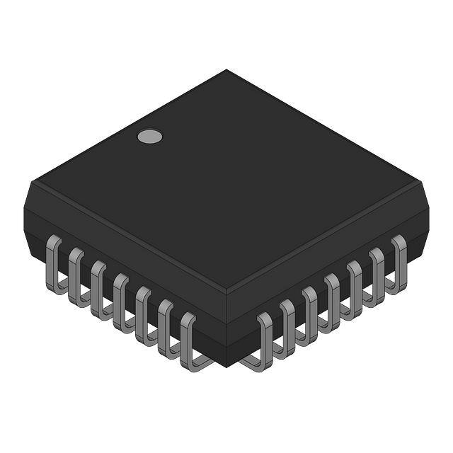
The AD9712 and AD9713 are available in 28-pin plastic DIPs and PLCCs, with an operating temperature range of 0 to + 70°C. Contact the factory for availability of military-grade devices.
c
0
Q' a
Q' Q
TE
~
w
o(191 YcONTROL I AMP IN
a:
C)
%
..
m:
iii
~ ~ 5~ C
;i
~
61 LATCH ENABLE
!I DIGITAL+V. REFERENCE GROUND
221 REFERENCE
GROUND
~
:2J REFERENCE OUT AMP IN AMP OUT IN
REFERENCE OUT
AMP IN
191 CONTROL
REFERENCE
,:' ,
51 ANALOG-V.
9 :!
..
'"
I- ,., Bwo
~
5
~.. ~ c:
II!
0
a. %::E
~
0 0
Plastic DIPPinout Designations (Top View)
PLCC Pinout Designations
REV.A
Information furnished by Analog Devices is believed to be accurate and reliable. However. no responsibility is assumed by Analog Devices for its use. nor for any infringements of patents or other rights of third parties which may result from its use. No license is granted by implication or otherwise under any patent or patent rights of Analog Devices.
One Technology Way. P.O. Box 9106. Norwood. MA 02062-9106 Tel: 617/329-4700 Fax: 617/326-8703 Twx: 710/394-6577 We5t CQut Central Atlantic: 714/641-9391 214/231-5094 215/643.7790
�RNRLOGDEVICES fRX-ON-DEnRND HOTLINE
- Page
2~
AD9712/AD9713 -SPECIFICATIONS
ABSOLUTE MAXIMUM RATINGS! Positive Supply Voltage (+Vs)(AD9713 Only) . . . . . . . .+6 V Negative Supply Voltage (-Vs) (AD9712andAD9713) 7V DAC Outputs to ANALOG RETURN . . . . . .+0.5 to -2 V V Digital Input Voltages (D1-D12' LATCH ENABLE) AD9712 0Vto-Vs AD9713 0Vto+Vs Internal Reference Output Current. . . . . - 20 JLAto + 500 fLA Control Amplifier Input Voltage Range . . . . . . . .0Vto -4 V ControlAmplifierOutputCurrent .:!:2.5mA REFERENCE IN Voltage Range. . . . . . . . . .-3.7 V to -Vs Analog Output Current (lOUT or lOUT) .30 mA Operating TemperatUre Range AD9712]NIJP Oto+70DC AD9713]N/]P Oto+70DC Maximum Junction Temperature2 . . . . . . . . . . . . . . .+ IS0.C Lead TemperatUre (Soldering, 10 seconds) . . . . . . . . .+ 300DC Storage TemperatUre Range .-65°C to + IS0DC
ELECTRICALCHARACTERISTICS (-Vs
= -5.2
V;+vs
OBS
Parameter (Conditions) RESOLUTION Temp DC ACCURACY Differential Nonlinearity Q) Integral Nonlinearity Q) «-------3S 1MHz SINE WAVE -40 -45 -50 .1!-55 .. -60 SPURIOUS-FREE DYNAMIC RANGE
-60
.1!-55 .. -4iO -M -7\) -7$ 10
L 4TH HARMONICS
,/ AT NOISE F1.00R I I 80 100 20 40 80 UPDATE RATE (lISPS)
i
2ND, 3RD, AND
CSFDR)
~
,/
-65 -70 -75 10
2ND, 3RD, AND 4TH HARMONICS AT NOI~E F1.00R I
i
60
60 100
AD9712 Harmonic Distortion vs. Update Rate
AD9713 Harmonic Distortion vs. Update Rate
-35 -40
-45
OBS -40 -45 -50
45
i--------
-so
i-55 -4iO -S L 3RO
-7\) -75
HARMONIC
i
10
20 40 80 UPDATERATE(MSPS)
AD9712 Harmonic Distortion vs. Update Rate
REFER
,-I
I
~
I -.. I_-tii
Output
CONTROL
~
OUT
OLE
.1!-55
-70 60 100 -7510
, , , .
.. -60 /2NDHARMONIC ~~:'~-:RMONIC -65 SADHARMONIC -
, 20 40 60 UPDATERATE(MSPS)
AD9713 Harmonic Distortion Ys. Update Rate
138 CURRENT SOUR
-
+
~
~~lLJ
Reference Input
TE
60 100
r
,
r---1
Reference
~~
~yf
ECLV-
-li.2Y
-li.2V
Control Amplifier Input
Full-Scale Current Control Loop
Control Amplifier Output
leu. "-
ECL Input Buffer
II
2R
2R II
II
"
2ft
"
2ft R
2.5kU
I"",
9
9
3OpI'
9
>2_1 -
TT1. IN
-$.2Y
R-2R DAC (for 6 LSBs)
-Va
ITL Input Buffer
Output Circut AD97121AD9713 Equivalent Circuits
REV. A
-7-
�ANALOGDEVICES FAX-ON-DEMANDHOTLINE
-
Page
30
AD971VAD9713
OUTLINE DIMENSIONS
Dimensions shown in inches and (rnm)
2S-Pin Plastic DIP (Suffix N)
0'> ex>
a
OBS
0.014111.112% (0.35610'-) D.IOOIISC (2.5411$C)
~I~= -11~._'~
~: : : : : : : : : : : ]~
1.38011.565 (35.101:1S.70) -10.01510.060 + + 0.1511
J ;I
~
~ (.)
t
IUI) MlN
H
~
D.70""X
(1.77 MAX)
t
Chip Carrier (Suffix P)
2S-Pin Plastic Leaded
LI- t ~~~:o;:~ ,..,
,(:4 ~ ii
~
!
TOP VIEW
~
(NOIIO-)
~
11
IZ
j.
(IU3i1t.S8) L..J OASOlG.- L.J U U L.J U 0---112.32112.57)
OLE
1
ae~
I
0.-430
f
...L (UI,:o.82)
0.lIIIO IISC
TII.Z7j) ...L 0.0131\).021
"
II
: LIO.Q2jIIO.03Z . IT (D.",,)
0.0"""-°25
T
(o.331G..53)
(o..3IW.63)
0.025I0.O«I(0.&411.01)
-o._nO(2.11112.79} -I O.le$;o.,OO 1(4.1"4.57)
TE
4. v> ::> ~ 0 UJ IZ a: 0..
-8-
REV. A
--~
�
很抱歉,暂时无法提供与“AD9713JP”相匹配的价格&库存,您可以联系我们找货
免费人工找货