10-/12-/14-Bit, 1200 MSPS DACS
AD9734/AD9735/AD9736
Data Sheet
FEATURES
FUNCTIONAL BLOCK DIAGRAM
RESET
DACCLK– DACCLK+
IRQ
S1 S2 S3
DATACLK_OUT+
DATACLK_OUT–
C1
CONTROLLER
SPI
C2
C3
LVDS
DRIVER
SDIO
SDO
CSB
SCLK
C3
CLOCK
DISTRIBUTION
DATACLK_IN+
DATACLK_IN–
DB[13:0]+
DB[13:0]–
SYNCHRONIZER
S3
LVDS
RECEIVER
2×
BAND GAP
C2
IOUTA
14-, 12-,
10-BIT DAC
CORE
REFERENCE
CURRENT
IOUTB
S2
C1S1
VREF
I120
04862-001
Pin-compatible family
Excellent dynamic performance
AD9736: SFDR = 82 dBc at fOUT = 30 MHz
AD9736: SFDR = 69 dBc at fOUT = 130 MHz
AD9736: IMD = 87 dBc at fOUT = 30 MHz
AD9736: IMD = 82 dBc at fOUT = 130 MHz
LVDS data interface with on-chip 100 Ω terminations
Built-in self test
LVDS sampling integrity
LVDS-to-DAC data transfer integrity
Low power: 380 mW (IFS = 20 mA; fOUT = 330 MHz)
1.8/3.3 V dual-supply operation
Adjustable analog output
8.66 mA to 31.66 mA (RL = 25 Ω to 50 Ω)
On-chip 1.2 V reference
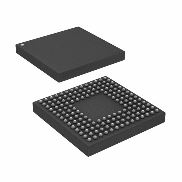
160-lead chip scale ball grid array (CSP_BGA) package
Figure 1.
APPLICATIONS
Broadband communications systems
Cellular infrastructure (digital predistortion)
Point-to-point wireless
CMTS/VOD
Instrumentation, automatic test equipment
Radar, avionics
PRODUCT HIGHLIGHTS
1.
2.
3.
GENERAL DESCRIPTION
The AD9736, AD9735, and AD9734 are high performance, high
frequency DACs that provide sample rates of up to 1200 MSPS,
permitting multicarrier generation up to their Nyquist
frequency. The AD9736 is the 14-bit member of the family,
while the AD9735 and the AD9734 are the 12-bit and 10-bit
members, respectively. They include a serial peripheral interface
(SPI) port that provides for programming of many internal
parameters and enables readback of status registers.
4.
5.
Low noise and intermodulation distortion (IMD) features
enable high quality synthesis of wideband signals at intermediate frequencies up to 600 MHz.
Double data rate (DDR) LVDS data receivers support the
maximum conversion rate of 1200 MSPS.
Direct pin programmability of basic functions or SPI port
access offers complete control of all AD973x family
functions.
Manufactured on a CMOS process, the AD973x family
uses a proprietary switching technique that enhances
dynamic performance.
The current output(s) of the AD9736 family are easily configured for single-ended or differential circuit topologies.
A reduced-specification LVDS interface is utilized to achieve
the high sample rate. The output current can be programmed
over a range of 8.66 mA to 31.66 mA. The AD973x family is
manufactured on a 0.18 µm CMOS process and operates from
1.8 V and 3.3 V supplies for a total power consumption of
380 mW in bypass mode. It is supplied in a 160-lead chip scale
ball grid array for reduced package parasitics.
Rev. B
Document Feedback
Information furnished by Analog Devices is believed to be accurate and reliable. However, no
responsibility is assumed by Analog Devices for its use, nor for any infringements of patents or other
rights of third parties that may result from its use. Specifications subject to change without notice. No
license is granted by implication or otherwise under any patent or patent rights of Analog Devices.
Trademarks and registered trademarks are the property of their respective owners.
One Technology Way, P.O. Box 9106, Norwood, MA 02062-9106, U.S.A.
Tel: 781.329.4700 ©2005–2017 Analog Devices, Inc. All rights reserved.
Technical Support
www.analog.com
�AD9734/AD9735/AD9736
Data Sheet
TABLE OF CONTENTS
Features .............................................................................................. 1
Applications ....................................................................................... 1
General Description ......................................................................... 1
Functional Block Diagram .............................................................. 1
Product Highlights ........................................................................... 1
Revision History ............................................................................... 3
Specifications..................................................................................... 4
DC Specifications ......................................................................... 4
Digital Specifications ................................................................... 6
AC Specifications.......................................................................... 8
Built-In Self Test Control (BIST_CNT) Registers (Reg. 17,
Reg. 18, Reg. 19, Reg. 20, Reg. 21) ........................................... 33
Controller Clock Predivider (CCLK_DIV) Reading Register
(Reg. 22)....................................................................................... 34
Theory of Operation ...................................................................... 35
Serial Peripheral Interface ............................................................. 36
General Operation of the Serial Interface ............................... 36
Short Instruction Mode (8-Bit Instruction) ........................... 36
Long Instruction Mode (16-Bit Instruction) .......................... 36
Serial Interface Port Pin Descriptions ..................................... 36
SCLK—Serial Clock ............................................................... 36
Absolute Maximum Ratings ............................................................ 9
CSB—Chip Select ................................................................... 37
Thermal Resistance ...................................................................... 9
SDIO—Serial Data I/O .......................................................... 37
Pin Configurations and Function Descriptions ......................... 10
Location of Supply and Control Pins ....................................... 16
Terminology .................................................................................... 17
Typical Performance Characteristics ........................................... 18
AD9736 Static Linearity, 10 mA Full Scale ............................. 18
AD9736 Static Linearity, 20 mA Full Scale ............................. 19
AD9736 Static Linearity, 30 mA Full Scale ............................. 20
AD9735 Static Linearity, 10 mA, 20 mA, 30 mA
Full Scale ...................................................................................... 21
SDO—Serial Data Out .......................................................... 37
MSB/LSB Transfers .................................................................... 37
Notes on Serial Port Operation ................................................ 37
Pin Mode Operation .................................................................. 38
RESET Operation ....................................................................... 38
Programming Sequence ............................................................ 38
Interpolation Filter ..................................................................... 39
Data Interface Controllers......................................................... 39
AD9734 Static Linearity, 10 mA, 20 mA, 30 mA
Full Scale ...................................................................................... 22
LVDS Sample Logic.................................................................... 40
AD9736 Power Consumption, 20 mA Full Scale ....................... 23
AD9736 Dynamic Performance, 20 mA Full Scale................ 24
Operating the LVDS Controller in Manual Mode via the
SPI Port ........................................................................................ 41
AD9735, AD9734 Dynamic Performance, 20 mA
Full Scale ...................................................................................... 27
Operating the LVDS Controller in Surveillance and Auto
Mode ............................................................................................ 41
AD973x WCDMA ACLR, 20 mA Full Scale .......................... 28
SYNC Logic and Controller .......................................................... 42
SPI Register Map ............................................................................. 29
SYNC Logic and Controller Operation ................................... 42
SPI Register Details ........................................................................ 30
Operation in Manual Mode ...................................................... 42
Mode Register (Reg. 0) .............................................................. 30
Operation in Surveillance and Auto Modes ........................... 42
Interrupt Request Register (IRQ) (Reg. 1) .............................. 30
FIFO Bypass ................................................................................ 42
Full Scale Current (FSC) Registers (Reg. 2, Reg. 3) ............... 31
Digital Built-In Self Test (BIST) ................................................... 44
LVDS Controller (LVDS_CNT) Registers (Reg. 4, Reg. 5,
Reg. 6) .......................................................................................... 31
Overview ..................................................................................... 44
SYNC Controller (SYNC_CNT) Registers (Reg. 7,
Reg. 8) .......................................................................................... 32
AD973x Expected BIST Signatures.......................................... 45
Cross Controller (CROS_CNT) Registers (Reg. 10,
Reg. 11) ........................................................................................ 32
Cross Controller Registers............................................................. 47
Analog Control (ANA_CNT) Registers (Reg. 14,
Reg. 15) ........................................................................................ 33
Band Gap Temperature Characteristic Trim Bits................... 48
LVDS Sample Logic Calibration............................................... 40
AD973x BIST Procedure ........................................................... 45
Generating Expected Signatures .............................................. 46
Analog Control Registers .............................................................. 48
Mirror Roll-Off Frequency Control ........................................ 48
Rev. B | Page 2 of 72
�Data Sheet
AD9734/AD9735/AD9736
Headroom Bits .............................................................................48
Input Data Timing .......................................................................... 54
Voltage Reference ........................................................................48
Synchronization Timing................................................................. 55
Applications Information ...............................................................50
Power Supply Sequencing .............................................................. 56
Driving the DACCLK Input ......................................................50
AD973X Evaluation Board Schematics ........................................ 57
DAC Output Distortion Sources ...................................................51
AD973X Evaluation Board PCB Layout ....................................... 62
DC-Coupled DAC Output .............................................................52
Outline Dimensions ........................................................................ 69
DAC Data Sources...........................................................................53
Ordering Guide ........................................................................... 69
REVISION HISTORY
6/2017—Rev. A to Rev. B
Change to SFLT Bit, Table 14 ..............................................32
Change to Data Interface Controller Section ..............................39
Changes to Figure 78 ......................................................................40
Changes to Figure 80 and Figure 81 .............................................41
Changes to AD793x BIST Signatures Section .............................45
Change to Generating Expected Signatures Section ..................46
Changes to Ordering Guide ...........................................................69
9/2006—Rev. 0 to Rev. A
Updated Format.................................................................. Universal
Changes to Table 1 ............................................................................ 5
Changes to Table 2 ............................................................................ 6
Changes to Table 3 ............................................................................ 8
Inserted Table 5.................................................................................. 9
Replaced Pin Configuration and Function Descriptions
Section .............................................................................................. 10
Changes to Figure 27 to Figure 38 ................................................ 21
Changes to Figure 40 ...................................................................... 23
Changes to Table 9 .......................................................................... 29
Changes to Figure 103 .................................................................... 56
Changes to Figure 105 .................................................................... 58
Changes to Figure 107 .................................................................... 60
Changes to Figure 108 .................................................................... 61
Changes to Figure 115 .................................................................... 68
Updated Outline Dimensions........................................................ 69
Changes to Ordering Guide ........................................................... 69
4/2005—Revision 0: Initial Version
Rev. B | Page 3 of 72
�AD9734/AD9735/AD9736
Data Sheet
SPECIFICATIONS
DC SPECIFICATIONS
AVDD33 = DVDD33 = 3.3 V, CVDD18 = DVDD18 = 1.8 V, maximum sample rate, IFS = 20 mA, 1× mode, 25 Ω, 1% balanced load,
unless otherwise noted.
Table 1.
Parameter
RESOLUTION
ACCURACY
Integral Nonlinearity (INL)
Differential Nonlinearity (DNL)
ANALOG OUTPUTS
Offset Error
Gain Error (With Internal
Reference)
Gain Error (Without Internal
Reference)
Full-Scale Output Current
Output Compliance Range
Output Resistance
Output Capacitance
TEMPERATURE DRIFT
Offset
Gain
Reference Voltage 1
REFERENCE
Internal Reference Voltage1
Output Resistance 2
ANALOG SUPPLY VOLTAGES
AVDD33
CVDD18
DIGITAL SUPPLY VOLTAGES
DVDD33
DVDD18
SUPPLY CURRENTS
1× Mode, 1.2 GSPS
IAVDD33
ICVDD18
IDVDD33
IDVDD18
FIR Bypass (1×) Mode
2× Mode, 1.2 GSPS
IAVDD33
ICVDD18
IDVDD33
IDVDD18
FIR 2× Interpolation Filter
Enabled
Min
AD9736
Typ
14
Max
Min
AD9735
Typ
12
Max
Min
AD9734
Typ
10
Max
Unit
Bits
−5.6
−2.1
±1.0
±0.6
+5.6
+2.1
−1.5
−0.5
±0.50
±0.25
+1.5
+0.5
−0.5
−0.1
±0.12
±0.06
+0.5
+0.1
LSB
LSB
−0.01
±0.005
±1.0
+0.01
−0.01
±0.005
±1.0
+0.01
−0.01
±0.005
±1.0
+0.01
% FSR
% FSR
±1.0
8.66
−1.0
20.2
±1.0
31.66
+1.0
8.66
−1.0
20.2
±1.0
31.66
1.0
8.66
−1.0
20.2
% FSR
31.66
+1.0
10
1
10
1
10
1
mA
V
MΩ
pF
0
80
40
0
80
40
0
80
40
ppm/°C
ppm/°C
ppm/°C
1.14
1.2
5
1.26
1.14
1.2
5
1.26
1.14
1.2
5
1.26
V
kΩ
3.13
1.70
3.3
1.8
3.47
1.90
3.13
1.70
3.3
1.8
3.47
1.90
3.13
1.70
3.3
1.8
3.47
1.90
V
V
3.13
1.70
3.3
1.8
3.47
1.90
3.13
1.70
3.3
1.8
3.47
1.90
3.13
1.70
3.3
1.8
3.47
1.90
V
V
25
47
10
122
380
25
47
10
122
380
25
47
10
122
380
mA
mA
mA
mA
mW
25
47
10
234
550
25
47
10
234
550
25
47
10
234
550
mA
mA
mA
mA
mW
Rev. B | Page 4 of 72
�Data Sheet
Parameter
Static, No Clock
IAVDD33
ICVDD18
IDVDD33
IDVDD18
FIR Bypass (1×) Mode
Sleep Mode, No Clock
IAVDD33
FIR Bypass (1×) Mode
Power-Down Mode 3
IAVDD33
ICVDD18
IDVDD33
IDVDD18
FIR Bypass (1×) Mode
AD9734/AD9735/AD9736
Min
AD9736
Typ
Max
25
8
10
2
133
Min
AD9735
Typ
Max
25
8
10
2
133
Min
AD9734
Typ
Max
25
8
10
2
133
Unit
mA
mA
mA
mA
mW
2.5
59
3.15
65
2.5
59
3.15
65
2.5
59
3.15
65
mA
mW
0.01
0.02
0.01
0.01
0.12
0.13
0.12
0.12
0.11
1.24
0.01
0.02
0.01
0.01
0.12
0.13
0.12
0.12
0.11
1.24
0.01
0.02
0.01
0.01
0.12
0.13
0.12
0.12
0.11
1.24
mA
mA
mA
mA
mW
Default band gap adjustment (Reg. 0x0E = 0x0).
Use an external amplifier to drive any external load.
3
Typical wake-up time is 8 µs with recommended 1 nF capacitor on VREF pin.
1
2
Rev. B | Page 5 of 72
�AD9734/AD9735/AD9736
Data Sheet
DIGITAL SPECIFICATIONS
AVDD33 = DVDD33 = 3.3 V, CVDD18 = DVDD18 = 1.8 V, maximum sample rate, IFS = 20 mA, 1× mode, 25 Ω, 1% balanced load,
unless otherwise noted. LVDS drivers and receivers are compliant to the IEEE-1596 reduced range link, unless otherwise noted.
Table 2.
Parameter
LVDS DATA INPUT
(DB[13:0]+, DB[13:0]−) DB+ = VIA, DB− = VIB
Input Voltage Range, VIA or VIB
Input Differential Threshold, VIDTH
Input Differential Hysteresis, VIDTHH − VIDTHL
Receiver Differential Input Impedance, RIN
LVDS Input Rate
LVDS Minimum Data Valid Period (tMDE)
LVDS CLOCK INPUT
(DATACLK_IN+, DATACLK_IN−) DATACLK_IN+ = VIA, DATACLK_IN− = VIB
Input Voltage Range, VIA or VIB
Input Differential Threshold, 1 VIDTH
Input Differential Hysteresis, VIDTHH − VIDTHL
Receiver Differential Input Impedance, RIN
Maximum Clock Rate
LVDS CLOCK OUTPUT
(DATACLK_OUT+, DATACLK_ OUT−) DATACLK_OUT+ = Voa, DATACLK_OUT− = Vob 100 Ω Termination
Output Voltage High, VOA or VOB
Output Voltage Low, VOA or VOB
Output Differential Voltage, |VOD|
Output Offset Voltage, VOS
Output Impedance, Single-Ended, RO
RO Mismatch Between A and B, ∆RO
Change in |VOD| Between 0 and 1, |∆VOD|
Change in VOS Between 0 and 1, ∆VOS
Output Current—Driver Shorted to Ground, ISA, ISB
Output Current—Drivers Shorted Together, ISAB
Power-Off Output Leakage, |IXA|, |IXB|
Maximum Clock Rate
DAC CLOCK INPUT (CLK+, CLK−)
Input Voltage Range, CLK− or CLK+
Differential Peak-to-Peak Voltage
Common-Mode Voltage
Maximum Clock Rate
SERIAL PERIPHERAL INTERFACE
Maximum Clock Rate (fSCLK, 1/tSCLK)
Minimum Pulse Width High, tPWH
Minimum Pulse Width Low, tPWL
Minimum SDIO and CSB to SCLK Setup, tDS
Minimum SCLK to SDIO Hold, tDH
Maximum SCLK to Valid SDIO and SDO, tDV
Minimum SCLK to Invalid SDIO and SDO, tDNV
Min
Typ
825
−100
Max
Unit
1575
+100
mV
mV
mV
Ω
MSPS
ps
20
80
1200
120
344
825
−100
1575
+100
20
80
600
120
1375
1025
150
1150
80
200
100
250
1250
120
10
25
25
20
4
10
600
0
400
300
1200
800
400
800
1600
500
20
20
20
10
5
20
5
Rev. B | Page 6 of 72
mV
mV
mV
Ω
MHz
mV
mV
mV
mV
Ω
%
mV
mV
mA
mA
mA
MHz
mV
mV
MHz
MHz
ns
ns
ns
ns
ns
ns
�Data Sheet
AD9734/AD9735/AD9736
Parameter
INPUT (SDI, SDIO, SCLK, CSB)
Voltage in High, VIH
Voltage in Low, VIL
Current in High, IIH
Current in Low, IIL
SDIO OUTPUT
Voltage out High, VOH
Voltage out Low, VOL
Current out High, IOH
Current out Low, IOL
Min
Max
Unit
−10
−10
0.8
+10
+10
V
V
µA
µA
2.4
0
3.6
0.4
2.0
Typ
3.3
0
4
4
Refer to the Input Data Timing section for recommended LVDS differential drive levels.
1
Rev. B | Page 7 of 72
V
V
mA
mA
�AD9734/AD9735/AD9736
Data Sheet
AC SPECIFICATIONS
AVDD33 = DVDD33 = 3.3 V, CVDD18 = DVDD18 = 1.8 V, maximum sample rate, IFS = 20 mA, 1× mode, 25 Ω, 1% balanced load,
unless otherwise noted.
Table 3.
Parameter
DYNAMIC PERFORMANCE
Maximum Update Rate
SPURIOUS-FREE DYNAMIC RANGE (SFDR)
fDAC = 800 MSPS
fOUT = 20 MHz
fDAC = 1200 MSPS
fOUT = 50 MHz
fOUT = 100 MHz
fOUT = 316 MHz
fOUT = 550 MHz
TWO-TONE INTERMODULATION
DISTORTION (IMD)
fDAC = 1200 MSPS
fOUT2 = fOUT + 1.25 MHz
fOUT = 40 MHz
fOUT = 50 MHz
fOUT = 100 MHz
fOUT = 316 MHz
fOUT = 550 MHz
NOISE SPECTRAL DENSITY (NSD)
Single Tone
fDAC = 1200 MSPS
fOUT = 50 MHz
fOUT = 100 MHz
fOUT = 241MHz
fOUT = 316 MHz
fOUT = 550 MHz
Eight-Tone
fDAC = 1200 MSPS, 500 kHz Tone Spacing
fOUT = 50 MHz
fOUT = 100 MHz
fOUT = 241MHz
fOUT = 316 MHz
fOUT = 550 MHz
Min
AD9736
Typ
1200
Max
Min
AD9735
Typ
Max
1200
Min
AD9734
Typ
Max
1200
Unit
MSPS
75
75
75
dBc
80
77
63
55
76
74
63
54
76
71
60
53
dBc
dBc
dBc
dBc
88
85
84
70.5
65
84
84
81
67
60
83
83
79
66
60
dBc
dBc
dBc
dBc
dBc
−158.5
−165
−164
−160.5
−158
−155
−162
−161
−159.5
−157
−155
−154
−154
−155
−152
−149
dBm/Hz
dBm/Hz
dBm/Hz
dBm/Hz
dBm/Hz
−163.3
−166.5
−166
−165
−164
−162
−163
−163
−161.5
−162
−160
−154
−152
−150.5
−151
−150
dBm/Hz
dBm/Hz
dBm/Hz
dBm/Hz
dBm/Hz
Rev. B | Page 8 of 72
�Data Sheet
AD9734/AD9735/AD9736
ABSOLUTE MAXIMUM RATINGS
Table 4.
Parameter
AVDD33
DVDD33
DVDD18
CVDD18
AVSS
AVSS
DVSS
CLK+, CLK−
PIN_MODE
DATACLK_IN,
DATACLK_OUT
LVDS Data Inputs
IOUTA, IOUTB
I120, VREF, IPTAT
IRQ, CSB, SCLK, SDO,
SDIO, RESET
Junction Temperature
Storage Temperature
With
Respect to
AVSS
DVSS
DVSS
CVSS
DVSS
CVSS
CVSS
CVSS
DVSS
DVSS
Min
−0.3 V
−0.3 V
−0.3 V
−0.3 V
−0.3 V
−0.3 V
−0.3 V
−0.3 V
−0.3 V
−0.3 V
Max
+3.6 V
+3.6 V
+1.98 V
+1.98 V
+0.3 V
+0.3 V
+0.3 V
CVDD18 + 0.18 V
DVDD33 + 0.3 V
DVDD33 + 0.3 V
DVSS
AVSS
AVSS
DVSS
−0.3 V
−1.0 V
−0.3 V
−0.3 V
DVDD33 + 0.3 V
AVDD33 + 0.3 V
AVDD33 + 0.3 V
DVDD33 + 0.3 V
−65°C
150°C
+150°C
Stresses at or above those listed under Absolute Maximum
Ratings may cause permanent damage to the product. This is a
stress rating only; functional operation of the product at these
or any other conditions above those indicated in the operational
section of this specification is not implied. Operation beyond
the maximum operating conditions for extended periods may
affect product reliability.
THERMAL RESISTANCE
θJA is specified for the worst-case conditions, that is, a device
soldered in a circuit board for surface-mount packages.
Table 5. Thermal Resistance
Package Type
160-Lead Ball, CSP_BGA
θJA measurement in still air.
1
ESD CAUTION
Rev. B | Page 9 of 72
θJA 1
31.2
Unit
°C/W
�AD9734/AD9735/AD9736
Data Sheet
PIN CONFIGURATIONS AND FUNCTION DESCRIPTIONS
1
2
3
4
5
6
7
8
9 10 11 12 13 14
A
B
C
D
DACCLK– E
DACCLK+ F
G
H
J
K
DB13 (MSB)
L
DB12
DB0 (LSB) M
DB11
N
04862-005
DB9
DB10
DB8
DB7
DB6
DATACLK_IN
DB5
DATACLK_OUT
DB4
DB3
DB2
DB1
P
Figure 2. AD9736 Digital LVDS Input, Clock I/O (Top View)
Table 6. AD9736 Pin Function Descriptions
Pin No.
A1, A2, A3, B1, B2, B3, C1, C2, C3, D2, D3
A4, A5, A6, A9, A10, A11, B4, B5, B6, B9,
B10, B11, C4, C5, C6, C9, C10, C11, D4, D5,
D6, D9, D10, D11
A7, B7, C7, D7
A8, B8, C8, D8
A12, A13, B12, B13, C12, C13, D12, D13
A14
B14
Mnemonic
CVDD18
AVSS
Description
1.8 V Clock Supply.
Analog Supply Ground.
IOUTB
IOUTA
AVDD33
DNC
I120
C14
VREF
D1, E2, E3, E4, F2, F3, F4, G1, G2, G3, G4
D14
CVSS
IPTAT
E1, F1
E11, E12, F11, F12, G11, G12
E13
DACCLK−/DACCLK+
AVSS
IRQ/UNSIGNED
E14
RESET/PD
F13
CSB/2×
F14
G13
G14
H1, H2, H3, H4, H11, H12, H13, H14, J1, J2,
J3, J4, J11, J12, J13, J14
SDIO/FIFO
SCLK/FSC0
SDO/FSC1
DVDD18
DAC Negative Output. 10 mA to 30 mA full-scale output current.
DAC Positive Output. 10 mA to 30 mA full-scale output current.
3.3 V Analog Supply.
Do Not Connect.
Nominal 1.2 V Reference. Tie to analog ground via 10 kΩ resistor to
generate a 120 μA reference current.
Band Gap Voltage Reference I/O. Tie to analog ground via 1 nF
capacitor; output impedance is approximately 5 kΩ.
Clock Supply Ground.
Factory Test Pin. Output current, proportional to absolute
temperature, is approximately 10 μA at 25°C with a slope of
approximately 20 nA/°C.
Negative/Positive DAC Clock Input (DACCLK).
Analog Supply Ground Shield. Tie to AVSS at the DAC.
If PIN_MODE = 0, IRQ: Active low open-drain interrupt request
output, pull up to DVDD33 with 10 kΩ resistor.
If PIN_MODE = 1, UNSIGNED: Digital input pin where 0 = twos
complement input data format, 1 = unsigned.
If PIN_MODE = 0, RESET: 1 resets the AD9736.
If PIN_MODE = 1, PD: 1 puts the AD9736 in the power-down state.
See the Serial Peripheral Interface section and the Pin Mode
Operation section for pin description.
See the Pin Mode Operation section for pin description.
See the Pin Mode Operation section for pin description.
See the Pin Mode Operation section for pin description.
1.8 V Digital Supply.
Rev. B | Page 10 of 72
�Data Sheet
AD9734/AD9735/AD9736
Pin No.
K1, K2, K3, K4, K11, K12, L2, L3, L4, L5, L6,
L9, L10, L11, L12, M3, M4, M5, M6, M9,
M10, M11, M12
K13, K14
Mnemonic
DVSS
Description
Digital Supply Ground.
DB−/DB+
L1
PIN_MODE
L7, L8, M7, M8, N7, N8, P7, P8
L13, L14
DVDD33
DB−/DB+
M2, M1
DB−/DB+
M13, M14
DB−/DB+
N1, P1
DB−/DB+
N2, P2
DB−/DB+
N3, P3
DB−/DB+
N4, P4
DB−/DB+
N5, P5
DB−/DB+
N6, P6
N10, P10
DATACLK_OUT−/
DATACLK_OUT+
DATACLK_IN−/
DATACLK_IN+
DB−/DB+
N11, P11
DB−/DB+
N12, P12
DB−/DB+
N13, P13
DB−/DB+
N14, P14
DB−/DB+
Negative/Positive Data Input Bit 13 (MSB). Conforms to IEEE-1596
reduced range link.
0 = SPI Mode. SPI is enabled.
1 = PIN Mode. SPI is disabled; direct pin control.
3.3 V Digital Supply.
Negative/Positive Data Input Bit 12. Conforms to IEEE-1596 reduced
range link.
Negative/Positive Data Input Bit 0 (LSB). Conforms to IEEE-1596
reduced range link.
Negative/Positive Data Input Bit 11. Conforms to IEEE-1596 reduced
range link.
Negative/Positive Data Input Bit 1. Conforms to IEEE-1596 reduced
range link.
Negative/Positive Data Input Bit 2. Conforms to IEEE-1596 reduced
range link.
Negative/Positive Data Input Bit 3. Conforms to IEEE-1596 reduced
range link.
Negative/Positive Data Input Bit 4. Conforms to IEEE-1596 reduced
range link.
Negative/Positive Data Input Bit 5. Conforms to IEEE-1596 reduced
range link.
Negative/Positive Data Output Clock. Conforms to IEEE-1596
reduced range link.
Negative/Positive Data Input Clock. Conforms to IEEE-1596 reduced
range link.
Negative/Positive Data Input Bit 6. Conforms to IEEE-1596 reduced
range link.
Negative/Positive Data Input Bit 7. Conforms to IEEE-1596 reduced
range link.
Negative/Positive Data Input Bit 8. Conforms to IEEE-1596 reduced
range link.
Negative/Positive Data Input Bit 9. Conforms to IEEE-1596 reduced
range link.
Negative/Positive Data Input Bit 10. Conforms to IEEE-1596 reduced
range link.
N9, P9
Rev. B | Page 11 of 72
�AD9734/AD9735/AD9736
Data Sheet
1
2
3
4
5
6
7
8
9 10 11 12 13 14
A
B
C
D
DACCLK– E
DACCLK+ F
G
H
J
K
DB11 (MSB)
L
DB10
DB9
NC M
N
04862-115
DB8
DB7
DB6
DB5
DB4
DATACLK_IN
DB3
DATACLK_OUT
DB1
DB2
NC
DB0 (LSB)
P
Figure 3. AD9735 Digital LVDS Input, Clock I/O (Top View)
Table 7. AD9735 Pin Function Descriptions
Pin No.
A1, A2, A3, B1, B2, B3, C1, C2, C3, D2, D3
A4, A5, A6, A9, A10, A11, B4, B5, B6, B9,
B10, B11, C4, C5, C6, C9, C10, C11, D4, D5,
D6, D9, D10, D11
A7, B7, C7, D7
A8, B8, C8, D8
A12, A13, B12, B13, C12, C13, D12, D13
A14
B14
Mnemonic
CVDD18
AVSS
Description
1.8 V Clock Supply.
Analog Supply Ground.
IOUTB
IOUTA
AVDD33
DNC
I120
C14
VREF
D1, E2, E3, E4, F2, F3, F4, G1, G2, G3, G4
D14
CVSS
IPTAT
E1, F1
E11, E12, F11, F12, G11, G12
E13
DACCLK−/DACCLK+
AVSS
IRQ/UNSIGNED
E14
RESET/PD
F13
CSB/2×
F14
G13
G14
H1, H2, H3, H4, H11, H12, H13, H14, J1, J2,
J3, J4, J11, J12, J13, J14
K1, K2, K3, K4, K11, K12, L2, L3, L4, L5, L6,
L9, L10, L11, L12, M3, M4, M5, M6, M9,
M10, M11, M12
SDIO/FIFO
SCLK/FSC0
SDO/FSC1
DVDD18
DAC Negative Output. 10 mA to 30 mA full-scale output current.
DAC Positive Output. 10 mA to 30 mA full-scale output current.
3.3 V Analog Supply.
Do Not Connect.
Nominal 1.2 V Reference. Tie to analog ground via 10 kΩ resistor to
generate a 120 µA reference current.
Band Gap Voltage Reference I/O. Tie to analog ground via 1 nF
capacitor; output impedance approximately 5 kΩ.
Clock Supply Ground.
Factory Test Pin; Output current, proportional to absolute
temperature, is approximately 10 µA at 25°C with a slope of
approximately 20 nA/°C.
Negative/Positive DAC Clock Input (DACCLK).
Analog Supply Ground Shield. Tie to AVSS at the DAC.
If PIN_MODE = 0, IRQ: Active low open-drain interrupt request
output, pull up to DVDD33 with 10 kΩ resistor.
If PIN_MODE = 1, UNSIGNED: Digital input pin where 0 = twos
complement input data format, 1 = unsigned.
If PIN_MODE = 0, RESET: 1 resets the AD9735.
If PIN_MODE = 1, PD: 1 puts the AD9735 in the power-down state.
See the Serial Peripheral Interface section and the Pin Mode
Operation section for pin description.
See the Pin Mode Operation section for pin description.
See the Pin Mode Operation section for pin description.
See the Pin Mode Operation section for pin description.
1.8 V Digital Supply.
DVSS
Digital Supply Ground.
Rev. B | Page 12 of 72
�Data Sheet
AD9734/AD9735/AD9736
Pin No.
K13, K14
Mnemonic
DB−/DB+
L1
PIN_MODE
L7, L8, M7, M8, N7, N8, P7, P8
L13, L14
DVDD33
DB−/DB+
M1, M2
M13, M14
NC
DB−/DB+
N1, P1
N2, P2
NC
DB−/DB+
N3, P3
DB−/DB+
N4, P4
DB−/DB+
N5, P5
DB−/DB+
N6, P6
N10, P10
DATACLK_OUT−/
DATACLK_OUT+
DATACLK_IN−/
DATACLK_IN+
DB−/DB+
N11, P11
DB−/DB+
N12, P12
DB−/DB+
N13, P13
DB−/DB+
N14, P14
DB−/DB+
N9, P9
Description
Negative/Positive Data Input Bit 11 (MSB). Conforms to IEEE-1596
reduced range link.
0 = SPI Mode. SPI is enabled.
1 = PIN Mode. SPI disabled; direct pin control.
3.3 V Digital Supply.
Negative/Positive Data Input Bit 10. Conforms to IEEE-1596 reduced
range link.
No Connect.
Negative/Positive Data Input Bit 9. Conforms to IEEE-1596 reduced
range link.
No Connect.
Negative/Positive Data Input Bit 0 (LSB). Conforms to IEEE-1596
reduced range link.
Negative/Positive Data Input Bit 1. Conforms to IEEE-1596 reduced
range link.
Negative/Positive Data Input Bit 2. Conforms to IEEE-1596 reduced
range link.
Negative/Positive Data Input Bit 3. Conforms to IEEE-1596 reduced
range link.
Negative/Positive Data Output Clock. Conforms to IEEE-1596
reduced range link.
Negative/Positive Data Input Clock. Conforms to IEEE-1596 reduced
range link.
Negative/Positive Data Input Bit 4. Conforms to IEEE-1596 reduced
range link.
Negative/Positive Data Input Bit 5. Conforms to IEEE-1596 reduced
range link.
Negative/Positive Data Input Bit 6. Conforms to IEEE-1596 reduced
range link.
Negative/Positive Data Input Bit 7. Conforms to IEEE-1596 reduced
range link.
Negative/Positive Data Input Bit 8. Conforms to IEEE-1596 reduced
range link.
Rev. B | Page 13 of 72
�AD9734/AD9735/AD9736
Data Sheet
1
2
3
4
5
6
7
8
9 10 11 12 13 14
A
B
C
D
DACCLK– E
DACCLK+ F
G
H
J
K
DB9 (MSB)
L
DB8
NC M
DB7
N
04862-114
DB6
DB5
DB4
DB3
DB2
DATACLK_IN
DB1
DATACLK_OUT
NC
DB0 (LSB)
NC
NC
P
Figure 4. AD9734 Digital LVDS Input, Clock I/O (Top View)
Table 8. AD9734 Pin Function Descriptions
Pin No.
A1, A2, A3, B1, B2, B3, C1, C2, C3, D2, D3
A4, A5, A6, A9, A10, A11, B4, B5, B6, B9,
B10, B11, C4, C5, C6, C9, C10, C11, D4, D5,
D6, D9, D10, D11
A7, B7, C7, D7
A8, B8, C8, D8
A12, A13, B12, B13, C12, C13, D12, D13
A14
B14
Mnemonic
CVDD18
AVSS
Description
1.8 V Clock Supply.
Analog Supply Ground.
IOUTB
IOUTA
AVDD33
DNC
I120
C14
VREF
D1, E2, E3, E4, F2, F3, F4, G1, G2, G3, G4
D14
CVSS
IPTAT
E1, F1
E11, E12, F11, F12, G11, G12
E13
DACCLK−/DACCLK+
AVSS
IRQ/UNSIGNED
E14
RESET/PD
F13
CSB/2×
F14
G13
G14
H1, H2, H3, H4, H11, H12, H13, H14, J1, J2,
J3, J4, J11, J12, J13, J14
K1, K2, K3, K4, K11, K12, L2, L3, L4, L5, L6,
L9, L10, L11, L12, M3, M4, M5, M6, M9,
M10, M11, M12
SDIO/FIFO
SCLK/FSC0
SDO/FSC1
DVDD18
DAC Negative Output. 10 mA to 30 mA full-scale output current.
DAC Positive Output. 10 mA to 30 mA full-scale output current.
3.3 V Analog Supply.
Do Not Connect.
Nominal 1.2 V Reference. Tie to analog ground via 10 kΩ resistor to
generate a 120 μA reference current.
Band Gap Voltage Reference I/O. Tie to analog ground via 1 nF
capacitor; output impedance approximately 5 kΩ.
Clock Supply Ground.
Factory Test Pin. Output current, proportional to absolute
temperature, is approximately 10 μA at 25°C with a slope of
approximately 20 nA/°C.
Negative/Positive DAC Clock Input (DACCLK).
Analog Supply Ground Shield. Tie to AVSS at the DAC.
If PIN_MODE = 0, IRQ: Active low open-drain interrupt request
output, pull up to DVDD33 with 10 kΩ resistor.
If PIN_MODE = 1, UNSIGNED: Digital input pin where 0 = twos
complement input data format, 1 = unsigned.
If PIN_MODE = 0, RESET: 1 resets the AD9734.
If PIN_MODE = 1, PD: 1 puts the AD9734 in the power-down state.
See the Serial Peripheral Interface section and the Pin Mode
Operation section for pin description.
See the Pin Mode Operation section for pin description.
See the Pin Mode Operation section for pin description.
See the Pin Mode Operation section for pin description.
1.8 V Digital Supply.
DVSS
Digital Supply Ground.
K13, K14
DB−/DB+
Negative/Positive Data Input Bit 9 (MSB). Conforms to IEEE-1596
Rev. B | Page 14 of 72
�Data Sheet
AD9734/AD9735/AD9736
Pin No.
Mnemonic
L1
PIN_MODE
L7, L8, M7, M8, N7, N8, P7, P8
L13, L14
DVDD33
DB−/DB+
M1, M2
M13, M14
NC
DB−/DB+
N1, P1
N2, P2
N3, P3
N4, P4
NC
NC
NC
DB−/DB+
N5, P5
DB−/DB+
N6, P6
N10, P10
DATACLK_OUT−/
DATACLK_OUT+
DATACLK_IN−/
DATACLK_IN+
DB−/DB+
N11, P11
DB−/DB+
N12, P12
DB−/DB+
N13, P13
DB−/DB+
N14, P14
DB−/DB+
N9, P9
Description
reduced range link.
0 = SPI Mode. SPI is enabled.
1 = PIN Mode. SPI is disabled; direct pin control.
3.3 V Digital Supply.
Negative/Positive Data Input Bit 8. Conforms to IEEE-1596 reduced
range link.
No Connect.
Negative/Positive Data Input Bit 7. Conforms to IEEE-1596 reduced
range link.
No Connect.
No Connect.
No Connect.
Negative/Positive Data Input Bit 0 (LSB). Conforms to IEEE-1596
reduced range link.
Negative/Positive Data Input Bit 1. Conforms to IEEE-1596 reduced
range link.
Negative/Positive Data Output Clock. Conforms to IEEE-1596
reduced range link.
Negative/Positive Data Input Clock. Conforms to IEEE-1596 reduced
range link.
Negative/Positive Data Input Bit 2. Conforms to IEEE-1596 reduced
range link.
Negative/Positive Data Input Bit 3. Conforms to IEEE-1596 reduced
range link.
Negative/Positive Data Input Bit 4. Conforms to IEEE-1596 reduced
range link.
Negative/Positive Data Input Bit 5. Conforms to IEEE-1596 reduced
range link.
Negative/Positive Data Input Bit 6. Conforms to IEEE-1596 reduced
range link.
Rev. B | Page 15 of 72
�AD9734/AD9735/AD9736
Data Sheet
LOCATION OF SUPPLY AND CONTROL PINS
4
5
6
7
8
9 10 11 12 13 14
1
A
A
B
B
C
C
D
D
E
E
F
F
G
G
H
H
J
J
K
K
L
L
M
M
N
N
P
P
AVDD33, 3.3V, ANALOG SUPPLY
AVSS, ANALOG SUPPLY GROUND SHIELD
2
3
4
5
6
7
8
4
5
6
7
8
9 10 11 12 13 14
DVDD33, 3.3V DIGITAL SUPPLY
DVSS DIGITAL SUPPLY GROUND
Figure 5. Analog Supply Pins (Top View)
1
3
DVDD18, 1.8V DIGITAL SUPPLY
04862-002
AVSS, ANALOG SUPPLY GROUND
2
04862-004
3
Figure 7. Digital Supply Pins (Top View)
9 10 11 12 13 14
A
B
1
C
2
3
4
5
6
IOUTA
2
IOUTB
1
7
8
9 10 11 12 13 14
D
A
E
B
I120
F
C
VREF
G
D
IPTAT
H
E
J
PIN_MODE =
SPI ENABLE
IRQ
RESE
F
K
CSB
SDIO
G
L
SCLK
SDO
H
J
N
K
P
PIN_MODE L
CVDD18, 1.8V CLOCK SUPPLY
CVSS, CLOCK SUPPLY GROUND
04862-003
M
PIN_MODE =
SPI DISABL
UNSIGNED
PD
M
2×
FIFO
N
FSC0
FSC1
P
Figure 6. Clock Supply Pins (Top View)
Figure 8. Analog I/O and SPI Control Pins (Top View)
Rev. B | Page 16 of 72
�Data Sheet
AD9734/AD9735/AD9736
TERMINOLOGY
Linearity Error (Integral Nonlinearity or INL)
The maximum deviation of the actual analog output from the
ideal output, determined by a straight line drawn from zero to
full scale.
Power Supply Rejection
The maximum change in the full-scale output as the supplies
are varied from nominal to minimum and maximum specified
voltages.
Differential Nonlinearity (DNL)
The measure of the variation in analog value, normalized to full
scale, associated with a 1 LSB change in digital input code.
Settling Time
The time required for the output to reach and remain within a
specified error band about its final value, measured from the
start of the output transition.
Monotonicity
A DAC is monotonic if the output either increases or remains
constant as the digital input increases.
Offset Error
The deviation of the output current from the ideal of zero. For
IOUTA, 0 mA output is expected when the inputs are all 0s. For
IOUTB, 0 mA output is expected when all inputs are set to 1s.
Gain Error
The difference between the actual and ideal output span. The
actual span is determined by the output when all inputs are set
to 1s minus the output when all inputs are set to 0s.
Output Compliance Range
The range of allowable voltage at the output of a current output
DAC. Operation beyond the maximum compliance limits can
cause either output stage saturation or breakdown, resulting in
nonlinear performance.
Temperature Drift
Specified as the maximum change from the ambient (25°C)
value to the value at either TMIN or TMAX. For offset and gain
drift, the drift is reported in ppm of full-scale range (FSR) per
°C. For reference drift, the drift is reported in ppm per °C.
Glitch Impulse
Asymmetrical switching times in a DAC give rise to undesired
output transients that are quantified by a glitch impulse. It is
specified as the net area of the glitch in pV-s.
Spurious-Free Dynamic Range
The difference, in dB, between the rms amplitude of the output
signal and the peak spurious signal over the specified
bandwidth.
Total Harmonic Distortion (THD)
The ratio of the rms sum of the first six harmonic components
to the rms value of the measured input signal. It is expressed as
a percentage or in decibels (dB).
Multitone Power Ratio
The spurious-free dynamic range containing multiple carrier
tones of equal amplitude. It is measured as the difference
between the rms amplitude of a carrier tone to the peak
spurious signal in the region of a removed tone.
Rev. B | Page 17 of 72
�AD9734/AD9735/AD9736
Data Sheet
TYPICAL PERFORMANCE CHARACTERISTICS
AD9736 STATIC LINEARITY, 10 mA FULL SCALE
1.00
1.0
0.75
0.8
0.50
0.6
0.25
0.4
ERROR (LSB)
ERROR (LSB)
0
–0.25
–0.50
–0.75
–1.00
0.2
0
–0.2
–0.4
–1.25
–0.6
–1.50
0
2048
4096
6144
8192 10240 12288 14336 16384
CODE
–1.0
04862-008
–2.00
0
Figure 9. AD9736 INL, −40°C, 10 mA FS
2048
4096
6144
8192 10240 12288 14336 16384
CODE
04862-010
–0.8
–1.75
Figure 12. AD9736 DNL, −40°C, 10 mA FS
1.00
1.0
0.75
0.8
0.50
0.6
0.25
0.4
ERROR (LSB)
ERROR (LSB)
0
–0.25
–0.50
–0.75
–1.00
0.2
0
–0.2
–0.4
–1.25
–0.6
–1.50
0
2048
4096
6144
8192 10240 12288 14336 16384
CODE
–1.0
04862-008
–2.00
0
Figure 10. AD9736 INL, 25°C, 10 mA FS
2048
4096
6144
8192 10240 12288 14336 16384
CODE
04862-011
–0.8
–1.75
Figure 13. AD9736 DNL, 25°C, 10 mA FS
1.00
1.0
0.75
0.8
0.50
0.6
0.25
0.4
ERROR (LSB)
–0.25
–0.50
–0.75
–1.00
0.2
0
–0.2
–0.4
–1.25
–0.6
–1.50
–2.00
0
2048
4096
6144
8192 10240 12288 14336 16384
CODE
Figure 11. AD9736 INL, 85°C, 10 mA FS
–1.0
0
2048
4096
6144
8192 10240 12288 14336 16384
CODE
Figure 14. AD9736 DNL, 85°C, 10 mA FS
Rev. B | Page 18 of 72
04862-012
–0.8
–1.75
04862-009
ERROR (LSB)
0
�Data Sheet
AD9734/AD9735/AD9736
0.6
0.8
0.5
0.6
0.4
0.4
0.3
0.2
0.2
0
–0.2
–0.4
–0.6
0.1
0
–0.1
–0.2
–0.8
–0.3
–1.0
–0.4
–1.2
–0.5
2048
4096
6144
8192 10240 12288 14336 16384
CODE
–0.6
0
0.6
0.8
0.5
0.6
0.4
0.4
0.3
0.2
0.2
ERROR (LSB)
1.0
0
–0.2
–0.4
–0.6
0
–0.2
–0.3
–0.4
–1.2
–0.5
2048
4096
6144
8192 10240 12288 14336 16384
CODE
–0.6
0
0.6
0.8
0.5
0.6
0.4
0.4
0.3
0.2
0.2
ERROR (LSB)
1.0
0
–0.2
–0.4
–0.6
–0.2
–0.4
–1.2
–0.5
6144
8192 10240 12288 14336 16384
CODE
8192 10240 12288 14336 16384
CODE
0
–0.3
4096
6144
–0.1
–1.0
2048
4096
0.1
–0.8
0
2048
Figure 19. AD9736 DNL, 25°C, 20 mA FS
04862-015
ERROR (LSB)
Figure 16. AD9736 INL, 25°C, 20 mA FS
–1.4
8192 10240 12288 14336 16384
CODE
–0.1
–1.0
0
6144
0.1
–0.8
–1.4
4096
Figure 18. AD9736 DNL, −40°C, 20 mA FS
04862-014
ERROR (LSB)
Figure 15. AD9736 INL, −40°C, 20 mA FS
2048
04862-017
0
Figure 17. AD9736 INL, 85°C, 20 mA FS
–0.6
0
2048
4096
6144
8192 10240 12288 14336 16384
CODE
Figure 20. AD9736 DNL, 85°C, 20 mA FS
Rev. B | Page 19 of 72
04862-018
–1.4
04862-016
ERROR (LSB)
1.0
04862-013
ERROR (LSB)
AD9736 STATIC LINEARITY, 20 mA FULL SCALE
�AD9734/AD9735/AD9736
Data Sheet
AD9736 STATIC LINEARITY, 30 mA FULL SCALE
0.6
2.0
0.5
1.5
0.4
0.3
1.0
ERROR (LSB)
ERROR (LSB)
0.2
0.5
0
–0.5
0.1
0
–0.1
–0.2
–0.3
–1.0
–0.4
–1.5
2048
4096
6144
8192 10240 12288 14336 16384
CODE
–0.6
04862-019
0
0
Figure 21. AD9736 INL, −40°C, 30 mA FS
2048
4096
6144
8192 10240 12288 14336 16384
CODE
04862-022
–0.5
–2.0
Figure 24. AD9736 DNL, −40°C, 30 mA FS
2.0
0.6
0.5
1.5
0.4
0.3
1.0
ERROR (LSB)
ERROR (LSB)
0.2
0.5
0
–0.5
0.1
0
–0.1
–0.2
–0.3
–1.0
–0.4
–1.5
2048
4096
6144
8192 10240 12288 14336 16384
CODE
–0.6
04862-020
0
0
Figure 22. AD9736 INL, 25°C, 30 mA FS
2048
4096
6144
8192 10240 12288 14336 16384
CODE
04862-023
–0.5
–2.0
Figure 25. AD9736 DNL, 25°C, 30 mA FS
2.0
1.0
1.5
0.5
1.0
0.5
0
0
ERROR (LSB)
0
0
–0.5
–0.5
–1.0
–0.5
–1.0
–1.5
–2.0
–1.0
–1.5
–2.5
–2.0
0
2048
4096
6144
8192 10240 12288 14336 16384
CODE
Figure 23. AD9736 INL, 85°C, 30 mA FS
–3.0
0
2048
4096
6144
8192 10240 12288 14336 16384
CODE
Figure 26. AD9736 DNL, 85°C, 30 mA FS
Rev. B | Page 20 of 72
04862-024
–1.5
04862-021
ERROR (LSB)
0
�Data Sheet
AD9734/AD9735/AD9736
AD9735 STATIC LINEARITY, 10 mA, 20 mA, 30 mA FULL SCALE
0.4
0.100
0.050
0.3
0
ERROR (LSB)
ERROR (LSB)
0.2
0.1
–0.050
–0.100
0
–0.150
–0.1
512
1024
1536
2048
CODE
2560
3072
3584
4096
–0.250
0
Figure 27. AD9735 INL, 25°C, 10 mA FS
512
1024
1536
2048
CODE
2560
3072
3584
4096
3584
4096
3584
4096
04862-028
0
04862-025
–0.2
–0.200
Figure 30. AD9735 DNL, 25°C, 10 mA FS
0.15
0.100
0.075
0.10
0.050
0.05
ERROR (LSB)
ERROR (LSB)
0.025
0
–0.05
0
–0.025
–0.050
–0.10
–0.075
–0.15
512
1024
1536
2048
2560
3072
3584
4096
CODE
–0.125
0
Figure 28. AD9735 INL, 25°C, 20 mA FS
0.050
0.1
0
1536
2048
CODE
2560
3072
–0.050
0
–1.000
ERROR (LSB)
–0.1
–0.2
–0.3
–1.150
–0.200
–0.250
–0.4
–0.300
–0.5
0
512
1024
1536
2048
CODE
2560
3072
3584
4096
Figure 29. AD9735 INL, 25°C, 30 mA FS
–0.400
0
512
1024
1536
2048
CODE
2560
3072
Figure 32. AD9735 DNL, 25°C, 30 mA FS
Rev. B | Page 21 of 72
04862-030
–0.350
04862-027
ERROR (LSB)
1024
Figure 31. AD9735 DNL, 25°C, 20 mA FS
0.2
–0.6
512
04862-029
0
04862-026
–0.20
–0.100
�AD9734/AD9735/AD9736
Data Sheet
AD9734 STATIC LINEARITY, 10 mA, 20 mA, 30 mA FULL SCALE
0.04
0.03
0.02
0.02
ERROR (LSB)
0.04
0
0.01
–0.02
0
–0.04
–0.01
0
128
256
512
384
640
768
896
04862-031
–0.06
1024
CODE
–0.02
0
128
256
384
512
CODE
640
768
896
1024
04862-034
ERROR (LSB)
0.06
Figure 36. AD9734 DNL, 25°C, 10 mA FS
Figure 33. AD9734 INL, 25°C, 10 mA FS
0.03
0.03
0.02
0.02
0.01
0.01
ERROR (LSB)
–0.01
–0.02
–0.03
0
–0.01
–0.04
–0.02
0
128
256
384
512
CODE
640
768
896
1024
–0.03
04862-032
–0.06
0
128
256
384
512
640
768
896
1024
CODE
04862-035
–0.05
Figure 37. AD9734 DNL, 25°C, 20 mA FS
Figure 34. AD9734 INL, 25°C, 20 mA FS
0.01
0.06
0.04
0
0.02
–0.01
ERROR (LSB)
0
–0.02
–0.04
–0.02
–0.03
–0.06
–0.04
–0.08
–0.12
0
128
256
384
512
CODE
640
768
896
1024
–0.06
0
128
256
384
512
CODE
640
768
Figure 38. AD9734 DNL, 25°C, 30 mA FS
Figure 35. AD9734 INL, 25°C, 30 mA FS
Rev. B | Page 22 of 72
896
1024
04862-036
–0.05
–0.10
04862-033
ERROR (LSB)
ERROR (LSB)
0
�Data Sheet
AD9734/AD9735/AD9736
AD9736 POWER CONSUMPTION, 20 mA FULL SCALE
0.7
0.50
0.45
0.6
TOTAL
0.40
TOTAL
0.5
0.25
0.20
DVDD18
0.15
0.4
DVDD18
0.3
CVDD18
0.2
AVDD33
0.10
DVDD33
0
0
250
500
750
fDAC (MHz)
1000
1250
1500
DVDD33
AVDD33
0.1
CVDD18
0.05
0
0
250
500
750
1000
1250
1500
fDAC (MHz)
Figure 40. AD9736, 2× Interpolation Mode Power vs. fDAC at 25°C
Figure 39. AD9736 1× Mode Power vs. fDAC at 25°C
Rev. B | Page 23 of 72
04862-038
POWER (W)
0.30
04862-037
POWER (W)
0.35
�AD9734/AD9735/AD9736
Data Sheet
80
75
800MSPS
IMD (dBc)
SFDR (dBc)
70
65
60
1.2GSPS
1GSPS
50
0
50
100 150 200 250 300 350 400 450 500 550 600
fOUT (MHz)
04862-039
55
92
90
88
86
84
82
80
78
76
74
72
70
68
66
64
62
60
58
0
50
100
150
200
250
300
350
400
450
500
550
fOUT (MHz)
Figure 41. AD9736 SFDR vs. fOUT over fDAC at 25°C
04862-042
AD9736 DYNAMIC PERFORMANCE, 20 mA FULL SCALE
Figure 44. AD9736 IMD vs. fOUT over 50 Parts, 25°C,1.2 GSPS
90
80
85
75
1GSPS
80
70
IMD (dBc)
SFDR (dBc)
75
65
+85°C
60
70
800MSPS
1.2GSPS
65
–40°C
60
+25°C
55
55
100 150 200 250 300 350 400 450 500 550 600
fOUT (MHz)
50
0
100
200
300
400
500
600
04862-043
50
600
04862-044
0
04862-040
50
fOUT (MHz)
Figure 42. AD9736 SFDR vs. fOUT over Temperature
Figure 45. AD9736 IMD vs. fOUT over fDAC at 25°C
90
78
76
85
74
80
72
75
IMD (dBc)
68
66
64
62
–40°C
70
+25°C
+85°C
65
60
58
60
56
55
54
52
0
50
100
150
200
250
300
350
400
450
500
550
fOUT (MHz)
50
04862-041
SFDR (dBc)
70
0
100
200
300
400
500
fOUT (MHz)
Figure 43. AD9736 SFDR vs. fOUT over 50 Parts, 25°C, 1.2 GSPS
Figure 46. AD9736 IMD vs. fOUT over Temperature, 1.2 GSPS
Rev. B | Page 24 of 72
�Data Sheet
AD9734/AD9735/AD9736
95
90
90
85
IMD
0dBFS
80
75
IMD (dBc)
SFDR
75
70
–6dBFS
65
65
60
60
55
55
0
10
fOUT (MHz)
100
–12dBFS
70
50
0
100
200
300
500
600
Figure 50. AD9736 IMD vs. fOUT over AOUT, 25°C, 1.2 GSPS
Figure 47. AD9736 Low Frequency IMD and SFDR vs. fOUT, 25°C, 1.2 GSPS
90
90
THIRD-ORDER IMD
85
SFDR_2×
SFDR
80
75
75
SFDR, IMD (dBc)
80
70
65
70
SFDR_1×
65
60
60
55
55
0
50
100
150
200
fOUT (MHz)
250
300
350
50
04862-046
50
Figure 48. AD9736 IMD and SFDR vs. fOUT, 25°C, 1.2 GSPS, 2× Interpolation
0
50
100
150
200
250
300
350
fOUT (MHz)
04862-049
85
SFDR, IMID (dBc)
400
fOUT (MHz)
04862-048
80
04862-045
IMD AND SFDR (dBc)
85
Figure 51. AD9736 SFDR vs. fOUT, 25°C, 1.2 GSPS, 1× and 2× Interpolation
80
90
75
85
THIRD-ORDER IMD_1×
70
80
–12dBFS
55
–6dBFS
70
65
50
60
45
55
40
0
100
200
300
fOUT (MHz)
400
500
600
Figure 49. AD9736 SFDR vs. fOUT over AOUT, 25°C, 1.2 GSPS
50
04862-047
SFDR (dBc)
0dBFS
60
75
0
50
100
150
200
fOUT (MHz)
250
300
350
04862-050
SFDR, IMD (dBc)
THIRD-ORDER IMD_2×
65
Figure 52. AD9736 IMD vs. fOUT, 25°C, 1.2 GSPS, 1× and 2× Interpolation
Rev. B | Page 25 of 72
�AD9734/AD9735/AD9736
Data Sheet
–150
–150
–152
–152
–154
–154
–156
–156
–160
–162
–158
–160
–164
–164
–166
–166
–168
–168
–170
0
100
200
300
fOUT (MHz)
400
500
600
+85°C
–162
–40°C
+25°C
–170
0
100
200
300
400
500
600
fOUT (MHz)
04862-054
NSD (dBm/Hz)
1.2GSPS
04862-051
NSD (dBm/Hz)
1GSPS
–158
Figure 56. AD9736 8-Tone NSD vs. fOUT over Temperature, 1.2 GSPS
Figure 53. AD9736 1-Tone NSD vs. fOUT over fDAC, 25°C
–150
–157
–152
–158
–154
–159
+85°C
–158
NSD (dBm/Hz)
–40°C
–160
+25°C
–162
–164
–160
–161
–162
–163
–164
–166
–165
–168
0
100
200
300
fOUT (MHz)
400
500
600
–166
04862-052
–170
0
50
100
150
200
250
300
350
400
450
500
550
fOUT (MHz)
Figure 54. AD9736 1-Tone NSD vs. fOUT over Temperature, 1.2 GSPS
04862-055
NSD (dBm/Hz)
–156
Figure 57. AD9736 1-Tone NSD vs. fOUT over 50 Parts, 1.2 GSPS, 25°C
–150
–161
–152
–154
–162
NSD (dBm/Hz)
–158
–160
–162
1GSPS
–163
–164
–165
–164
1.2GSPS
–166
–166
–170
0
100
200
300
fOUT (MHz)
400
500
600
–167
Figure 55. AD9736 8-Tone NSD vs. fOUT over fDAC, 25°C
0
50
100
150
200
250
300
fOUT (MHz)
350
400
450
500
550
04862-056
–168
04862-053
NSD (dBm/Hz)
–156
Figure 58. AD9736 8-Tone NSD vs. fOUT over 50 Parts, 1.2 GSPS, 25°C
Rev. B | Page 26 of 72
�Data Sheet
AD9734/AD9735/AD9736
AD9735, AD9734 DYNAMIC PERFORMANCE, 20 mA FULL SCALE
80
90
85
75
1GSPS
80
800MSPS
75
IMD (dBc)
SFDR (dBc)
70
65
60
800MSPS
70
1.2GSPS
65
1GSPS
60
0
50
100 150 200 250 300 350 400 450 500 550 600
fOUT (MHz)
50
04862-060
50
55
1.2GSPS
0
Figure 59. AD9735 SFDR vs. fOUT over fDAC, 1.2 GSPS
50
100 150 200 250 300 350 400 450 500 550 600
fOUT (MHz)
04862-063
55
Figure 62. AD9734 IMD vs. fOUT over fDAC, 1.2 GSPS
80
–150
–152
75
–154
–156
NSD (dBc/Hz)
800MSPS
65
1GSPS
60
–160
–162
8 TONES
–166
1.2GSPS
0
50
100 150 200 250 300 350 400 450 500 550 600
fOUT (MHz)
–168
–170
0
50
Figure 60. AD9734 SFDR vs. fOUT over fDAC, 1.2 GSPS
Figure 63. AD9735 NSD vs. fOUT, 1.2 GSPS
90
–145
1GSPS
–147
85
–149
80
800MSPS
8 TONES
–151
NSD (dBc/Hz)
75
70
65
1.2GSPS
–153
1 TONE
–155
–157
–159
60
–161
55
0
50
100 150 200 250 300 350 400 450 500 550 600
fOUT (MHz)
Figure 61. AD9735 IMD vs. fOUT over fDAC, 1.2 GSPS
–165
0
50
100 150 200 250 300 350 400 450 500 550 600
fOUT (MHz)
Figure 64. AD9734 NSD vs. fOUT, 1.2 GSPS
Rev. B | Page 27 of 72
04862-065
–163
50
04862-062
IMD (dBc)
100 150 200 250 300 350 400 450 500 550 600
fOUT (MHz)
04862-064
55
50
1 TONE
–158
–164
04862-061
SFDR (dBc)
70
�AD9734/AD9735/AD9736
Data Sheet
AD973x WCDMA ACLR, 20 mA FULL SCALE
REF –22.75dBm
#AVG
LOG 10dB/
04862-057
#ATTEN 6dB
PAVG
10
W1
S2
CENTER 134.83MHz
#RES BW 30kHz
RMS RESULTS
CARRIER POWER
–10.72dBm/
3.84000MHz
VBW 300kHz
OFFSET FREQ
5.00MHz
10.0MHz
15.0MHz
REF BW
3.840MHz
3.840MHz
3.884MHz
LOWER
dBc
dBm
–81.65
–92.37
–82.06
–92.78
–82.11
–92.83
SPAN 33.88MHz
SWEEP 109.9ms (601pts)
UPPER
dBc
–81.39
–82.43
–82.39
dBm
–92.11
–93.16
–93.11
Figure 65. AD9736 WCDMA Carrier at 134.83 MHz, fDAC = 491.52 MSPS
REF –22.75dBm
#AVG
LOG 10dB/
04862-058
#ATTEN 6dB
PAVG
10 S2
CENTER 134.83MHz
#RES BW 30kHz
RMS RESULTS
CARRIER POWER
–10.72dBm/
3.84000MHz
VBW 300kHz
OFFSET FREQ
5.00MHz
10.0MHz
15.0MHz
REF BW
3.840MHz
3.840MHz
3.884MHz
LOWER
dBc
dBm
–80.32
–91.10
–81.13
–91.91
–80.43
–91.21
SPAN 33.88MHz
SWEEP 109.9ms (601pts)
UPPER
dBc
–80.60
–80.75
–81.36
dBm
–91.38
–91.53
–92.13
Figure 66. AD9735 WCDMA Carrier at 134.83 MHz, fDAC = 491.52 MSPS
REF –22.75dBm
#AVG
LOG 10dB/
04862-059
#ATTEN 6dB
PAVG
10 S2
CENTER 134.83MHz
#RES BW 30kHz
RMS RESULTS
CARRIER POWER
–10.76dBm/
3.84000MHz
VBW 300kHz
OFFSET FREQ
5.00MHz
10.0MHz
15.0MHz
SPAN 33.88MHz
SWEEP 109.9ms (601pts)
REF BW
3.840MHz
3.840MHz
3.884MHz
LOWER
dBc
dBm
–71.07
–81.83
–70.55
–81.31
–70.79
–81.56
UPPER
dBc
–71.23
–71.42
–71.25
dBm
–81.99
–82.19
–82.01
Figure 67. AD9734 WCDMA Carrier at 134.83 MHz, fDAC = 491.52 MSPS
Rev. B | Page 28 of 72
�Data Sheet
AD9734/AD9735/AD9736
SPI REGISTER MAP
Write 0 to unspecified or reserved bit locations. Reading these bits returns unknown values.
Table 9. SPI Register Map
Reg. Addr.
Dec.
0
1
2
3
4
5
6
7
8
9
10
11
12
13
14
15
16
17
18
19
20
21
22
Hex.
00
01
02
03
04
05
06
07
08
09
0A
0B
0C
0D
0E
0F
10
11
12
13
14
15
16
Name
Bit 7
Bit 6
Bit 5
Bit 4
Bit 3
Bit 2
Bit 1
Bit 0
Default
(Hex)
Pin Mode
(Hex)
MODE
IRQ
FSC_1
FSC_2
LVDS_CNT1
LVDS_CNT2
LVDS_CNT3
SYNC_CNT1
SYNC_CNT2
RESERVED
CROS_CNT1
CROS_CNT2
RESERVED
RESERVED
ANA_CNT1
ANA_CNT2
RESERVED
BIST_CNT
BIST
BIST
BIST
BIST
CCLK_DIV
SDIO_DIR
LVDS
SLEEP
FSC
MSD
SD
LSURV
FIFOSTAT3
SSURV
LSBFIRST
SYNC
RESET
CROSS
LONG_INS
RESERVED
2X MODE
IE_LVDS
FIFO MODE
IE_SYNC
FSC
MSD
SD
LAUTO
FIFOSTAT2
SAUTO
FSC
MSD
SD
LFLT
FIFOSTAT1
SFLT
FSC
MSD
SD
LFLT
FIFOSTAT0
SFLT
FSC
MHD
LCHANGE
LFLT
VALID
SFLT
FSC
MHD
ERR_HI
LFLT
SCHANGE
SFLT
DATAFRMT
IE_CROSS
FSC
FSC
MHD
ERR_LO
LTRH
PHOF
RESERVED
PD
RESERVED
FSC
FSC
MHD
CHECK
LTRH
PHOF
STRH
00
00
02
00
00
00
00
00
00
00
00
02
00
00
00
00
00
00
UPDEL
DNDEL
UPDEL
DNDEL
UPDEL
DNDEL
UPDEL
DNDEL
UPDEL
DNDEL
UPDEL
DNDEL
00
00
00
00
HDRM
HDRM
TRMBG
HDRM
TRMBG
HDRM
TRMBG
HDRM
C0
CA
C0
CA
LVDS_EN
SYNC_EN
CLEAR
00
00
CCD
CCD
CCD
00
00
MSEL
HDRM
MSEL
HDRM
HDRM
SEL
SEL
SIG_READ
RESERVED
RESERVED
RESERVED
RESERVED
CCD
Rev. B | Page 29 of 72
�AD9734/AD9735/AD9736
Data Sheet
SPI REGISTER DETAILS
Reading these registers returns previously written values for all defined register bits, unless otherwise noted. Reset value for write registers
in bold text.
MODE REGISTER (REG. 0)
ADDR
0x00
Name
MODE
Bit 7
SDIO_DIR
Bit 6
LSB/MSB
Bit 5
RESET
Bit 4
LONG_INS
Bit 3
2× MODE
Bit 2
FIFO MODE
Bit 1
DATAFRMT
Bit 0
PD
Table 10. Mode Register Bit Descriptions
Bit Name
SDIO_DIR
Read/Write
WRITE
LSB/MSB
WRITE
RESET
WRITE
LONG_INS
WRITE
2×_MODE
WRITE
FIFO_MODE
WRITE
DATAFRMT
WRITE
PD
WRITE
Description
0, input only per SPI standard.
1, bidirectional per SPI standard.
0, MSB first per SPI standard.
1, LSB first per SPI standard.
NOTE: Only change LSB/MSB order in single-byte instructions to avoid erratic behavior due to bit
order errors.
0, execute software reset of SPI and controllers, reload default register values except Registers 0x00
and 0x04.
1, set software reset, write 0 on the next (or any following) cycle to release the reset.
0, short (single-byte) instruction word.
1, long (two-byte) instruction word, not necessary since the maximum internal address is REG31
(0x1F).
0, disable 2× interpolation filter.
1, enable 2× interpolation filter.
0, disable FIFO synchronization.
1, enable FIFO synchronization.
0, signed input DATA with midscale = 0x0000.
1, unsigned input DATA with midscale = 0x2000.
0, enable LVDS Receiver, DAC, and clock circuitry.
1, power down LVDS Receiver, DAC, and clock circuitry.
INTERRUPT REQUEST REGISTER (IRQ) (REG. 1)
ADDR
0x01
Name
IRQ
Bit 7
LVDS
Bit 6
SYNC
Bit 5
CROSS
Bit 4
RESERVED
Bit 3
IE_LVDS
Bit 2
IE_SYNC
Table 11. Interrupt Register Bit Descriptions
Bit Name
LVDS
Read/Write
WRITE
READ
SYNC
WRITE
READ
CROSS
WRITE
READ
IE_LVDS
WRITE
IE_SYNC
WRITE
IE_CROSS
WRITE
Description
Don’t care.
0, no active LVDS receiver interrupt.
1, interrupt in LVDS receiver occurred.
Don’t care.
0, no active SYNC logic interrupt.
1, interrupt in SYNC logic occurred.
Don’t care.
0, no active CROSS logic interrupt.
1, interrupt in CROSS logic occurred.
0, reset LVDS receiver interrupt and disable future LVDS receiver interrupts.
1, enable LVDS receiver interrupt to activate IRQ pin.
0, reset SYNC logic interrupt and disable future SYNC logic interrupts.
1, enable SYNC logic interrupt to activate IRQ pin.
0, reset CROSS logic interrupt and disable future CROSS logic interrupts.
1, enable CROSS logic interrupt to activate IRQ pin.
Rev. B | Page 30 of 72
Bit 1
IE_CROSS
Bit 0
RESERVED
�Data Sheet
AD9734/AD9735/AD9736
FULL SCALE CURRENT (FSC) REGISTERS (REG. 2, REG. 3)
ADDR
0x02
0x03
Name
FSC_1
FSC_2
Bit 7
SLEEP
FSC
Bit 6
–
FSC
Bit 5
Bit 4
Bit 3
Bit 2
–
FSC
–
FSC
–
FSC
–
FSC
Bit 1
FSC
FSC
Bit 0
FSC
FSC
Table 12. Full Scale Current Output Register Bit Descriptions
Bit Name
SLEEP
Read/Write
WRITE
FSC
WRITE
Description
0, enable DAC output.
1, set DAC output current to 0 mA.
0x000, 10 mA full-scale output current.
0x200, 20 mA full-scale output current.
0x3FF, 30 mA full-scale output current.
LVDS CONTROLLER (LVDS_CNT) REGISTERS (REG. 4, REG. 5, REG. 6)
ADDR
0x04
0x05
0x06
Name
LVDS_CNT1
LVDS_CNT2
LVDS_CNT3
Bit 7
MSD
SD
LSURV
Bit 6
MSD
SD
LAUTO
Bit 5
MSD
SD
LFLT
Bit 4
MSD
SD
LFLT
Bit 3
MHD
LCHANGE
LFLT
Bit 2
MHD
ERR_HI
LFLT
Bit 1
MHD
ERR_LO
LTRH
Bit 0
MHD
CHECK
LTRH
Table 13. LVDS Controller Register Bit Descriptions
Bit Name
MSD
Read/Write
WRITE
READ
MHD
WRITE
READ
SD
WRITE
READ
LCHANGE
READ
ERR_HI
ERR_LO
CHECK
READ
READ
READ
LSURV
WRITE
LAUTO
WRITE
LFLT
WRITE
LTRH
WRITE
Description
0x0, set setup delay for the measurement system.
If ( LAUTO = 1), the latest measured value for the setup delay.
If ( LAUTO = 0), readback of the last SPI write to this bit.
0x0, set hold delay for the measurement system.
If ( LAUTO = 1), the latest measured value for the hold delay.
If ( LAUTO = 0), readback of the last SPI write to this bit.
0x0, set sample delay.
If ( LAUTO = 1), the result of a measurement cycle is stored in this register.
If ( LAUTO = 0), readback of the last SPI write to this bit.
0, no change from previous measurement.
1, change in value from the previous measurement.
NOTE: The average filter and the threshold detection are not applied to this bit.
One of the 15 LVDS inputs is above the input voltage limits of the IEEE reduced link specification.
One of the 15 LVDS inputs is below the input voltage limits of the IEEE reduced link specification.
0, phase measurement—sampling in the previous or following DATA cycle.
1, phase measurement—sampling in the correct DATA cycle.
0, the controller stops after completion of the current measurement cycle.
1, continuous measurements are taken and an interrupt is issued if the clock alignment drifts beyond the
threshold value.
0, sample delay is not automatically updated.
1, continuously starts measurement cycles and updates the sample delay according to the measurement.
NOTE: LSURV (Reg. 6, Bit 7) must be set to 1 and the LVDS IRQ (Reg. 1, Bit 3) must be set to 0 for AUTO mode.
0x0, average filter length, Delay = Delay + Delta Delay/2^ LFLT , values greater than 12 (0x0C) are
clipped to 12.
000, set auto update threshold values.
Rev. B | Page 31 of 72
�AD9734/AD9735/AD9736
Data Sheet
SYNC CONTROLLER (SYNC_CNT) REGISTERS (REG. 7, REG. 8)
ADDR
0x07
0x08
Name
SYNC_CNT1
SYNC_CNT2
Bit 7
FIFOSTAT3
SSURV
Bit 6
FIFOSTAT2
SAUTO
Bit 5
FIFOSTAT1
SFLT
Bit 4
FIFOSTAT0
SFLT
Bit 3
VALID
SFLT
Bit 2
SCHANGE
SFLT
Bit 1
PHOF
RESERVED
Bit 0
PHOF
STRH
Table 14. Sync Controller Register Bit Descriptions
Bit Name
FIFOSTAT
FIFOSTAT
Read/Write
READ
READ
VALID
READ
SCHANGE
READ
PHOF
WRITE
READ
SSURV
WRITE
SAUTO
WRITE
SFLT
WRITE
STRH
WRITE
Description
Position of FIFO read counter ranges from 0 to 7.
0, SYNC logic OK.
1, error in SYNC logic.
0, FIFOSTAT is not valid yet.
1, FIFOSTAT is valid after a reset.
0, no change in FIFOSTAT.
1, FIFOSTAT has changed since the previous measurement cycle when SSURV = 1 (surveillance mode
active).
00, change the readout counter.
Current setting of the readout counter (PHOF) in surveillance mode (SSURV = 1) after an interrupt.
Current calculated optimal readout counter value in AUTO mode (SAUTO = 1).
0, the controller stops after completion of the current measurement cycle.
1, continuous measurements are taken and an interrupt is issued if the readout counter drifts beyond the
threshold value.
0, readout counter (PHOF) is not automatically updated.
1, continuously starts measurement cycles and updates the readout counter according to the
measurement.
NOTE: SSURV (Reg. 8, Bit 7) must be set to 1 and the SYNC IRQ (Reg. 1, Bit 2) must be set to 0 for AUTO
mode.
0x0, average filter length, FIFOSTAT = FIFOSTAT + Delta FIFOSTAT/2 ^ SFLT; values greater than 12
(0x0C) are not valid.
0, if FIFOSTAT = 0 or 7, a sync interrupt is generated.
1, if FIFOSTAT = 0, 1, 6 or 7, a sync interrupt is generated.
CROSS CONTROLLER (CROS_CNT) REGISTERS (REG. 10, REG. 11)
ADDR
0x0A
0x0B
Name
CROS_CNT1
CROS_CNT2
Bit 7
–
–
Bit 6
–
–
Bit 5
UPDEL
DNDEL
Bit 4
UPDEL
DNDEL
Bit 3
UPDEL
DNDEL
Bit 2
UPDEL
DNDEL
Bit 1
UPDEL
DNDEL
Table 15. Cross Controller Register Description
Bit Name
UPDEL
DNDEL
Read/Write
WRITE
WRITE
Description
0x00, move the differential output stage switching point up, set to 0 if DNDEL is non-zero.
0x00, move the differential output stage switching point down, set to 0 if UPDEL is non-zero.
Rev. B | Page 32 of 72
Bit 0
UPDEL
DNDEL
�Data Sheet
AD9734/AD9735/AD9736
ANALOG CONTROL (ANA_CNT) REGISTERS (REG. 14, REG. 15)
ADDR
0x0E
0x0F
Name
ANA_CNT1
ANA_CNT2
Bit 7
MSEL
HDRM
Bit 6
MSEL
HDRM
Bit 5
–
HDRM
Bit 4
–
HDRM
Bit 3
–
HDRM
Bit 2
TRMBG
HDRM
Bit 1
TRMBG
HDRM
Bit 0
TRMBG
HDRM
Table 16. Analog Control Register Bit Descriptions
Bit Name
MSEL
Read/Write
WRITE
Description
TRMBG
WRITE
000, band gap temperature characteristic trim.
NOTE: See the plot in the Analog Control Registers section.
HDRM
WRITE
0xCA, output stack headroom control.
HDRM set reference offset from AVDD33 (VCAS centering).
HDRM set overdrive (current density) trim (temperature tracking).
Note: Set to 0xCA for optimum performance.
00, mirror roll off frequency control = bypass.
01, mirror roll off frequency control = narrowest bandwidth.
10, mirror roll off frequency control = medium bandwidth.
11, mirror roll off frequency control = widest bandwidth.
NOTE: See the plot in the Analog Control Registers section.
BUILT-IN SELF TEST CONTROL (BIST_CNT) REGISTERS (REG. 17, REG. 18, REG. 19, REG. 20, REG. 21)
ADDR
0x11
0x12
0x13
0x14
0x15
Name
BIST_CNT
BIST
BIST
BIST
BIST
Bit 7
SEL
BIST
BIST
BIST
BIST
Bit 6
SEL
BIST
BIST
BIST
BIST
Bit 5
SIG_READ
BIST
BIST
BIST
BIST
Bit 4
–
BIST
BIST
BIST
BIST
Bit 3
–
BIST
BIST
BIST
BIST
Bit 2
LVDS_EN
BIST
BIST
BIST
BIST
Table 17. BIST Control Register Bit Descriptions
Bit Name
SEL
Read/Write
WRITE
SIG_READ
WRITE
LVDS_EN
WRITE
SYNC_EN
WRITE
CLEAR
WRITE
BIST
READ
Description
00, write result of the LVDS Phase 1 BIST to BIST.
01, write result of the LVDS Phase 2 BIST to BIST.
10, write result of the SYNC Phase 1 BIST to BIST.
11, write result of the SYNC Phase 2 BIST to BIST.
0, no action.
1, enable BIST signature readback.
0, no action.
1, enable LVDS BIST.
0, no action.
1, enable SYNC BIST.
0, no action.
1, clear all BIST registers.
Results of the built-in self test.
Rev. B | Page 33 of 72
Bit 1
SYNC_EN
BIST
BIST
BIST
BIST
Bit 0
CLEAR
BIST
BIST
BIST
BIST
�AD9734/AD9735/AD9736
Data Sheet
CONTROLLER CLOCK PREDIVIDER (CCLK_DIV) READING REGISTER (REG. 22)
ADR
0x16
Name
CCLK_DIV
Bit 7
RESERVED
Bit 6
RESERVED
Bit 5
RESERVED
Bit 4
RESERVED
Bit 3
CCD
Bit 2
CCD
Bit 1
CCD
Bit 0
CCD
Table 18. Controller Clock Predivider Register Bit Descriptions
Bit Name
CCD
Read/Write
WRITE
Description
0x0, controller clock = DACCLK/16.
0x1, controller clock = DACCLK/32.
0x2, controller clock = DACCLK/64 …
0xF, controller clock = DACCLK/524288.
NOTE: The 100 MHz to 1.2 GHz DACCLK must be divided to less than 10 MHz for correct operation. CCD
must be programmed to divide the DACCLK so that this relationship is not violated. Controller clock =
DACCLK/(2 ^ ( CCD + 4 )).
Rev. B | Page 34 of 72
�Data Sheet
AD9734/AD9735/AD9736
THEORY OF OPERATION
The AD9736, AD9735, and AD9734 are 14-bit, 12-bit, and
10-bit DACs that run at an update rate up to 1.2 GSPS. Input
data can be accepted up to the full 1.2 GSPS rate, or a 2×
interpolation filter can be enabled (2× mode) allowing full
speed operation with a 600 MSPS input data rate. The DATA
and DATACLK_IN inputs are parallel LVDS, meeting the IEEE
reduced swing LVDS specifications with the exception of input
hysteresis. The DATACLK_IN input runs at one-half the input
DATA rate in a double data rate (DDR) format. Each edge of
DATACLK_IN transfers DATA into the AD9736, as shown in
Figure 79.
The DACCLK−/DACCLK+ inputs (Pin E1 and Pin F1) directly
drive the DAC core to minimize clock jitter. The DACCLK
signal is also divided by 2 (1× and 2× mode), then output as the
DATACLK_OUT. The DATACLK_OUT signal clocks the data
source. The DAC expects DDR LVDS data (DB) aligned
with the DDR input clock (DATACLK_IN) from a circuit similar to the one shown in Figure 96. Table 19 shows the clock
relationships.
Table 19. AD973x Clock Relationship
MODE
1×
2×
DACCLK
1.2 GHz
1.2 GHz
DATACLK_OUT
600 MHz
600 MHz
DATACLK_IN
600 MHz
300 MHz
DATA
1.2 GSPS
600 MSPS
Maintaining correct alignment of data and clock is a common
challenge with high speed DACs, complicated by changes in
temperature and other operating conditions. Using the
DATACLK_OUT signal to generate the data allows most of the
internal process, temperature, and voltage delay variation to be
cancelled. The AD973x further simplifies this high speed data
capture problem with two adaptive closed-loop timing
controllers.
The LVDS controller locates the data transitions and delays the
DATACLK_IN so that its transition is in the center of the valid
data window. The sync controller manages the FIFO that moves
data from the LVDS DATACLK_IN domain to the DACCLK
domain.
Both controllers can operate in manual mode under external
processor control, in surveillance mode where error conditions
generate external interrupts, or in automatic mode where errors
are automatically corrected.
The LVDS and sync controllers include moving average filtering
for noise immunity and variable thresholds to control activity.
Normally, the controllers are set to run in automatic mode,
making any necessary adjustments without dropping or duplicating samples sent to the DAC. Both controllers require initial
calibration prior to entering automatic update mode.
The AD973x analog output changes 35 DACCLK cycles after
the input data changes in 1× mode with the FIFO disabled. The
FIFO adds up to eight additional cycles of delay. This delay is
read from the SPI port. Internal clock delay variation is less
than a single DACCLK cycle at 1.2 GHz (833 ps).
Stopping the AD973x DATACLK_IN while the DACCLK is still
running can lead to unpredictable output signals. This occurs
because the internal digital signal path is interleaved. The last
two samples clocked into the DAC continue to be clocked out
by DACCLK even after DATACLK_IN has stopped. The resulting output signal is at a frequency of one-half fDAC, and the
amplitude depends on the difference between the last two
samples.
Control of the AD973x functions is via the serially programmed
registers listed in Table 9. Optionally, a limited number of functions can be directly set by external pins in pin mode.
One timing controller manages the LVDS data and data clock
alignment (LVDS controller), and the other manages the LVDS
data and DACCLK alignment (sync controller).
Rev. B | Page 35 of 72
�AD9734/AD9735/AD9736
Data Sheet
SERIAL PERIPHERAL INTERFACE
The AD973x serial port is a flexible, synchronous serial
communications port, allowing easy interface to many
industry-standard microcontrollers and microprocessors. The
serial I/O is compatible with most synchronous transfer
formats, including both the Motorola SPI® and Intel® SSR
protocols. The interface allows read/write access to all registers
that configure the AD973x. Single- or multiple-byte transfers
are supported, as well as most significant bit first (MSB-first) or
least significant bit first (LSB-first) transfer formats. The
AD973x serial interface port can be configured as a single pin
I/O (SDIO) or two unidirectional pins for in/out (SDIO/SDO).
SDO (PIN G14)
SCLK (PIN G13)
AD973x
SPI PORT
CSB (PIN F13)
04862-066
SDIO (PIN F14)
MSB
I7
R/W
I6
N1
I5
N0
I4
A4
I3
A3
I2
A2
I1
A1
LSB
I0
A0
R/W, Bit 7 of the instruction byte, determines whether a read or
a write data transfer occurs after the instruction byte write.
Logic high indicates read operation. Logic 0 indicates a write
operation. N1, N0, Bit 6, and Bit 5 of the instruction byte
determine the number of bytes to be transferred during the data
transfer cycle. The bit decodes are shown in Table 20.
A4, A3, A2, A1, A0, Bit 4, Bit 3, Bit 2, Bit 1, and Bit 0 of the
instruction byte, determine which register is accessed during
the data transfer portion of the communications cycle. For
multibyte transfers, this address is the starting byte address. The
remaining register addresses are generated by the AD973x,
based on the LSBFIRST bit (Reg. 0, Bit 6).
Table 20. Byte Transfer Count
Figure 68. AD973x SPI Port
The AD973x can optionally be configured via external pins
rather than the serial interface. When the PIN_MODE input
(Pin L1) is high, the serial interface is disabled and its pins are
reassigned for direct control of the DAC. Specific functionality
is described in the Pin Mode Operation section.
GENERAL OPERATION OF THE SERIAL INTERFACE
There are two phases to a communication cycle with the
AD973x. Phase 1 is the instruction cycle, which is the writing of
an instruction byte into the AD973x, coincident with the first
eight SCLK rising edges. The instruction byte provides the
AD973x serial port controller with information regarding the
data transfer cycle, which is Phase 2 of the communication
cycle. The Phase 1 instruction byte defines whether the
upcoming data transfer is read or write, the number of bytes in
the data transfer, and the starting register address for the first
byte of the data transfer. The first eight SCLK rising edges of
each communication cycle are used to write the instruction byte
into the AD973x.
The remaining SCLK edges are for Phase 2 of the communication cycle. Phase 2 is the actual data transfer between the
AD973x and the system controller. Phase 2 of the communication cycle is a transfer of 1, 2, 3, or 4 data bytes as determined
by the instruction byte. Using one multibyte transfer is the
preferred method. Single-byte data transfers are useful to
reduce CPU overhead when register access requires one byte
only. Registers change immediately upon writing to the last bit
of each transfer byte.
N1
0
0
1
1
N2
0
1
0
1
Description
Transfer 1 byte
Transfer 2 bytes
Transfer 3 bytes
Transfer 4 bytes
LONG INSTRUCTION MODE (16-BIT INSTRUCTION)
The long instruction bytes are shown in the following table:
MSB
I15
R/W
I7
A7
I14
N1
I6
A6
I13
N0
I5
A5
I12
A12
I4
A4
I11
A11
I3
A3
I10
A10
I2
A2
I9
A9
I1
A1
LSB
I8
A8
I0
A0
If LONG_INS = 1 (Reg. 0, Bit 4), the instruction byte is
extended to 2 bytes where the second byte provides an
additional 8 bits of address information. Address 0x00 to
Address 0x1F are equivalent in short and long instruction
modes. The AD973x does not use any addresses greater than 31
(0x1F), so always set LONG_INS = 0.
SERIAL INTERFACE PORT PIN DESCRIPTIONS
SCLK—Serial Clock
The serial clock pin is used to synchronize data to and from the
AD973x and to run the internal state machines. The maximum
frequency of SCLK is 20 MHz. All data input to the AD973x is
registered on the rising edge of SCLK. All data is driven out of
the AD973x on the rising edge of SCLK.
CSB (Chip Select) can be raised after each sequence of 8 bits
(except the last byte) to stall the bus. The serial transfer resumes
when CSB is lowered. Stalling on nonbyte boundaries resets
the SPI.
SHORT INSTRUCTION MODE (8-BIT INSTRUCTION)
The short instruction byte is shown in the following table:
Rev. B | Page 36 of 72
�Data Sheet
AD9734/AD9735/AD9736
CSB—Chip Select
Active low input starts and gates a communication cycle. It
allows more than one device to be used on the same serial
communications lines. The SDO and SDIO pins go to a high
impedance state when this input is high. Chip select should stay
low during the entire communication cycle.
SDIO—Serial Data I/O
Data is always written into the AD973x on this pin. However,
this pin can be used as a bidirectional data line. The configuration of this pin is controlled by SDIO_DIR at Reg. 0, Bit 7.
The default is Logic 0, which configures the SDIO pin as
unidirectional.
SDO—Serial Data Out
Data is read from this pin for protocols that use separate lines
for transmitting and receiving data. In the case where the
AD973x operates in a single bidirectional I/O mode, this pin
does not output data and is set to a high impedance state.
MSB/LSB TRANSFERS
For multibyte transfers, writing to this register can occur during
the middle of the communication cycle. Care must be taken to
compensate for this new configuration for the remaining bytes
of the current communication cycle. The same considerations
apply to setting the software reset, RESET (Reg. 0, Bit 5). All
registers are set to their default values except Reg. 0 and Reg. 4,
which remain unchanged.
Use of only single-byte transfers when changing serial port
configurations or initiating a software reset is highly
recommended. In the event of unexpected programming
sequences, the AD973x SPI can become inaccessible. For
example, if user code inadvertently changes the LONG_INS bit
or the LSBFIRST bit, the following bits experience unexpected
results. The SPI can be returned to a known state by writing an
incomplete byte (1 to 7 bits) of all 0s followed by 3 bytes of
0x00. This returns to MSB-first short instructions
(Reg. 0 = 0x00), so the device can be reinitialized.
INSTRUCTION CYCLE
DATA TRANSFER CYCLE
CSB
When LSBFIRST = 1 (LSB first), the instruction and data bytes
must be written from least significant bit to most significant bit.
Multibyte data transfers in LSB-first format start with an
instruction byte that includes the register address of the least
significant data byte followed by multiple data bytes. The serial
port internal byte address generator increments for each byte of
the multibyte communication cycle.
The AD973x serial port controller data address decrements
from the data address written toward 0x00 for multibyte I/O
operations if the MSB-first mode is active. The serial port
controller address increments from the data address written
toward 0x1F for multibyte I/O operations if the LSB-first mode
is active.
NOTES ON SERIAL PORT OPERATION
R/W N1 N0 A4 A3
A2 A1 A0 D7N D6N D5N
D30 D20 D10 D00
04862-067
SDIO
Figure 69. Serial Register Interface Timing, MSB-First Write
INSTRUCTION CYCLE
DATA TRANSFER CYCLE
CSB
SCLK
SDIO
R/W N1 N0 A4 A3
A2 A1 A0
D6N D5N
D30 D20 D10 D00
D6N D5N
D30 D20 D10 D00
D7
SDO
04862-068
When LSBFIRST = 0 (MSB first), the instruction and data bytes
must be written from the most significant bit to the least
significant bit. Multibyte data transfers in MSB-first format start
with an instruction byte that includes the register address of the
most significant data byte. Subsequent data bytes should follow
in order from high address to low address. In MSB-first mode,
the serial port internal byte address generator decrements for
each data byte of the multibyte communication cycle.
SCLK
D7
Figure 70. Serial Register Interface Timing, MSB-First Read
INSTRUCTION CYCLE
DATA TRANSFER CYCLE
CSB
SCLK
SDIO
A0
A1 A2 A3
A4 N0
N1 R/W D00 D10 D20
D4N D5N D6N D7N
04862-069
The AD973x serial port can support both MSB-first or LSB-first
data formats. This functionality is controlled by LSBFIRST at
Reg. 0, Bit 6. The default is MSB first (LSBFIRST = 0).
Figure 71. Serial Register Interface Timing, LSB-First Write
INSTRUCTION CYCLE
DATA TRANSFER CYCLE
CSB
SCLK
SDIO
A0 A1 A2 A3
A4
N0
N1 R/W
D10 D20
D4N D5N D6N D7N
D10 D20
D4N D5N D6N D7N
D0
SDO
D0
Figure 72. Serial Register Interface Timing, LSB-First Read
Rev. B | Page 37 of 72
04862-070
The AD973x serial port configuration is controlled by Reg. 0,
Bit 4, Bit 5, Bit 6, and Bit 7. Note that the configuration changes
immediately upon writing to the last bit of the register.
�AD9734/AD9735/AD9736
tDS
Data Sheet
tSCLK
Table 22. PIN_MODE Input Functions
Mnemonic
UNSIGNED
CSB
tPWH
tPWL
SCLK
2×
tDH
INSTRUCTION BIT 7
SDIO
04862-071
tDS
INSTRUCTION BIT 6
FSC1, FSC0
Figure 73. Timing Diagram for SPI Register Write
CSB
PD
tDNV
SDIO I1
I0
D7
tDV
D6
D5
04862-072
SCLK
Figure 74. Timing Diagram for SPI Register Read
After the last instruction bit is written to the SDIO pin, the
driving signal must be set to a high impedance in time for the
bus to turn around. The serial output data from the AD973x is
enabled by the falling edge of SCLK. This causes the first output
data bit to be shorter than the remaining data bits, as shown in
Figure 74.
To assure proper reading of data, read the SDIO or SDO pin
prior to changing the SCLK from low to high. Due to the more
complex multibyte protocol, multiple AD973x devices cannot
be daisy-chained on the SPI bus. Multiple DACs should be
controlled by independent CSB signals.
PIN MODE OPERATION
When the PIN_MODE input (Pin L1) is set high, the SPI port is
disabled. The SPI port pins are remapped, as shown in Table 21.
The function of these pins is described in Table 22. The remaining PIN_MODE register settings are shown in Table 9.
Table 21. SPI_MODE vs. PIN_MODE Inputs
Pin Number
E13
F13
G13
E14
F14
G14
PIN_MODE = 0
IRQ
CSB
SCLK
RESET
SDIO
SDO
PIN_MODE = 1
UNSIGNED
2×
FSC0
PD
FIFO
FSC1
FIFO
Function
0, twos complement input data format
1, unsigned input data format
0, interpolation disabled
1, interpolation = 2× enabled
00, sleep mode
01, 10 mA full-scale output current
10, 20 mA full-scale output current
11, 30 mA full-scale output current
0, chip enabled
1, chip in power-down state
0, input FIFO disabled
1, input FIFO enabled
Care must be taken when using PIN_MODE because only the
control bits shown in Table 22 can be changed. If the remaining
register default values are not suitable for the desired operation,
PIN_MODE cannot be used. If the FIFO is enabled, the
controller clock must be less than 10 MHz. This limits the DAC
clock to 160 MHz.
RESET OPERATION
The RESET pin forces all SPI register contents to their default
values (see Table 9), which places the DAC in a known state.
The software reset bit forces all SPI register contents, except
Reg. 0 and Reg. 4, to their default values.
The internal reset signal is derived from a logical OR operation
on the RESET pin state and from the software reset state. This
internal reset signal drives all SPI registers to their default
values, except Reg. 0 and Reg. 4, which are unaffected. The data
registers are not affected by either reset.
The software reset is asserted by writing 1 to Reg. 0, Bit 5. It
may be cleared on the next SPI write cycle or a later write cycle.
PROGRAMMING SEQUENCE
The AD973x registers should be programmed in this order:
1.
2.
3.
4.
5.
6.
7.
Reset hardware.
Make changes to SPI port configuration, if necessary.
Input format, if unsigned.
Interpolation, if in 2× mode.
Calibrate and set the LVDS controller.
Enable the FIFO.
Calibrate and set the sync controller.
Step 1 through Step 4 are required, while Step 5 through Step 7
are optional. The LVDS controller can help assure proper data
reception in the DAC with changes in temperature and voltage.
The sync controller manages the FIFO to assure proper transfer
of the received data to the DAC core with changes in
temperature and voltage. The DAC is intended to operate with
both controllers active unless data and clock alignment is
managed externally.
Rev. B | Page 38 of 72
�Data Sheet
AD9734/AD9735/AD9736
INTERPOLATION FILTER
0.10
In 2× mode, the input data is interpolated by a factor of 2 so
that it aligns with the DAC update rate. The interpolation filter
is a hard-coded, 55-tap, symmetric FIR with a 0.001 dB passband flatness and a stop-band attenuation of about 90 dB. The
transition band runs from 20% of fDAC to 30% of fDAC. The FIR
response is shown in Figure 75 where the frequency axis is
normalized to fDAC. Figure 76 shows the pass-band flatness and
Table 23 shows the 16-bit filter coefficients.
0.08
0.06
MAGNITUDE (dB)
0.04
0.02
0
–0.02
–0.04
Table 23. FIR Interpolation Filter Coefficients
–0.08
Coefficient Number
1
2
3
4
5
6
7
8
9
10
11
12
13
14
15
16
17
18
19
20
21
22
23
24
25
26
27
28
–0.10
Tap Weight
−7
0
+24
0
−62
0
+135
0
−263
0
+471
0
−793
0
+1273
0
−1976
0
+3012
0
−4603
0
+7321
0
−13270
0
+41505
+65535
0
0.25
Figure 76. Interpolation Filter Pass-Band Flatness
DATA INTERFACE CONTROLLERS
Two internal controllers are utilized in the operation of the
AD973x. The first controller helps maintain optimum LVDS
data sampling; the second controller helps maintain optimum
synchronization between the DACCLK and the incoming data.
The LVDS controller is responsible for optimizing the sampling
of the data from the LVDS bus (DB13:0), while the sync
controller resolves timing problems between the DAC_CLK
(CLK+, CLK−) and the DATACLK. A block diagram of these
controllers is shown in Figure 77.
DATACLK
DATACLK_OUT
CLK
CONTROL
DATACLK_IN
DATA
SOURCE
i.e., FPGA
LVDS
CONTROLLER
SYNC
CONTROLLER
SYNC
LOGIC
LVDS
SAMPLE
LOGIC
DB
FIFO
DAC
Figure 77. Data Controllers
The controllers are clocked with a divided-down version of the
DAC_CLK. The divide ratio is set utilizing the controller clock
predivider bits (CCD) located at Reg. 22, Bits 3:0 to
generate the controller clock as follows:
Controller Clock = DAC_CLK/(2^(CCD + 4))
–10
Note that the controller clock cannot exceed 10 MHz for correct
operation. Until CCD is properly programmed to meet
this requirement, the DAC output may not be stable. This
means the FIFO cannot be enabled in PIN_MODE unless the
DACCLK is less than 160 MHz.
–20
–30
–40
–50
–60
–70
–80
–90
–100
0
0.05
0.10 0.15 0.20 0.25 0.30 0.35 0.40
FREQUENCY NORMALIZED TO fDAC
0.45
0.50
04862-073
MAGNITUDE (dB)
0.20
0.15
0.05
0.10
FREQUENCY NORMALIZED TO fDAC
0
04862-075
Coefficient Number
55
54
53
52
51
50
49
48
47
46
45
44
43
42
41
40
39
38
37
36
35
34
33
32
31
30
29
04862-074
–0.06
Figure 75. Interpolation Filter Response
Rev. B | Page 39 of 72
�AD9734/AD9735/AD9736
Data Sheet
DBU
The LVDS and sync controllers are independently operated in
three modes via SPI port Reg. 6 and Reg. 8:
FF
D1
FF
D2
DBL
DATA SAMPLING
SIGNAL
In surveillance mode, each controller takes measurements and
calculates a new optimal value continuously. The result of the
measurement is passed through an averaging filter before
evaluating the results for increased noise immunity. The filtered
result is compared to a threshold value set via Reg. 6 and Reg. 8
of the SPI port. If the error is greater than the threshold, an
interrupt is triggered and the controller stops.
DELAYED
CLOCK
SIGNAL
SD
SAMPLE DELAY
In manual mode, all of the timing measurements and updates
are externally controlled via the SPI.
DATACLK_IN
LVDS
RX
MSD
DELAY
CHECK
FF
MHD
DELAY
CLOCK
SAMPLING
SIGNAL
04862-076
Manual mode
Surveillance mode
Auto mode
Figure 78. Internal LVDS Data Sampling Logic
CLK TO DB SKEW
Reg. 1 of the SPI port controls the interrupts with Bit 3 and Bit 2
enabling the respective interrupts and Bit 7 and Bit 6 indicating
the respective controller interrupt. If an interrupt is enabled, it
also activates the AD973x IRQ pin. To clear an interrupt, the
interrupt enable bit of the respective controller must be set to 0
for at least 1 controller clock cycle (controller clock