IF Digitizing Subsystem
AD9864
Data Sheet
FEATURES
GENERAL DESCRIPTION
10 MHz to 300 MHz input frequency
6.8 kHz to 270 kHz output signal bandwidth
7.5 dB single sideband noise figure (SSB NF)
−7.0 dBm input third-order intercept (IIP3)
AGC free range up to −34 dBm
12 dB continuous AGC range
16 dB front-end attenuator
Baseband I/Q 16-bit (or 24-bit) serial digital output
LO and sampling clock synthesizers
Programmable decimation factor, output format, AGC, and
synthesizer settings
370 Ω input impedance
2.7 V to 3.6 V supply voltage
Low current consumption: 17 mA
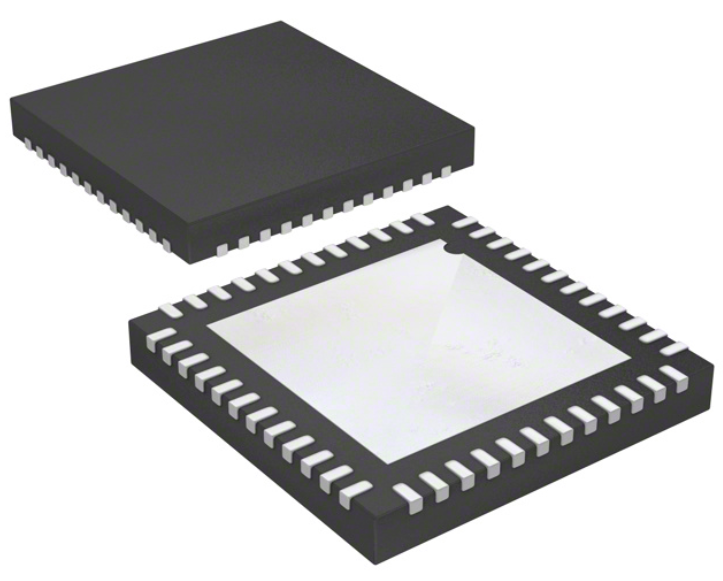
48-lead LFCSP package
The AD98641 is a general-purpose IF subsystem that digitizes a
low level, 10 MHz to 300 MHz IF input with a signal bandwidth
ranging from 6.8 kHz to 270 kHz. The signal chain of the AD9864
consists of a low noise amplifier (LNA), a mixer, a band-pass Σ-∆
analog-to-digital converter (ADC), and a decimation filter with
programmable decimation factor. An automatic gain control
(AGC) circuit gives the AD9864 12 dB of continuous gain
adjustment. Auxiliary blocks include both clock and local
oscillator (LO) synthesizers.
The high dynamic range of the AD9864 and inherent antialiasing
provided by the band-pass Σ-∆ converter allow the device to cope
with blocking signals up to 95 dB stronger than the desired signal.
This attribute often reduces the cost of a radio by reducing IF
filtering requirements. Also, it enables multimode radios of varying
channel bandwidths, allowing the IF filter to be specified for the
largest channel bandwidth.
APPLICATIONS
The SPI port programs numerous parameters of the AD9864,
allowing the device to be optimized for any given application.
Programmable parameters include synthesizer divide ratios, AGC
attenuation and attack/decay time, received signal strength level,
decimation factor, output data format, 16 dB attenuator, and the
selected bias currents.
Multimode narrow-band radio products
Analog/digital UHF/VHF FDMA receivers
TETRA, APCO25, GSM/EDGE
Portable and mobile radio products
SATCOM terminals
The AD9864 is available in a 48-lead LFCSP package and operates
from a single 2.7 V to 3.6 V supply. The total power consumption
is typically 56 mW and a power-down mode is provided via
serial interfacing.
FUNCTIONAL BLOCK DIAGRAM
MXOP MXON IF2P IF2N
GCP GCN
DAC
AD9864
AGC
–16dB
IFIN
LNA
DECIMATION
FILTER
Σ-Δ ADC
FORMATTING/SSI
DOUTA
DOUTB
FS
CLKOUT
FREF
CONTROL LOGIC
LO
SYN
LOP LON
LO VCO AND
LOOP FILTER
IOUTC
CLKP
CLKN
VREFP VCM VREFN
SPI
PC
PD
PE
SYNCB
04319-0-001
IOUTL
VOLTAGE
REFERENCE
CLK SYN
LOOP FILTER
Figure 1.
1
Protected by U.S. Patent No. 5,969,657; other patents pending.
Rev. A
Document Feedback
Information furnished by Analog Devices is believed to be accurate and reliable. However, no
responsibility is assumed by Analog Devices for its use, nor for any infringements of patents or other
rights of third parties that may result from its use. Specifications subject to change without notice. No
license is granted by implication or otherwise under any patent or patent rights of Analog Devices.
Trademarks and registered trademarks are the property of their respective owners.
One Technology Way, P.O. Box 9106, Norwood, MA 02062-9106, U.S.A.
Tel: 781.329.4700 ©2003–2016 Analog Devices, Inc. All rights reserved.
Technical Support
www.analog.com
�AD9864
Data Sheet
TABLE OF CONTENTS
Features .............................................................................................. 1
SSI Control Registers ................................................................. 21
Applications ....................................................................................... 1
Synchronization Using SYNCB ................................................ 24
General Description ......................................................................... 1
Interfacing to DSPs .................................................................... 24
Functional Block Diagram .............................................................. 1
Power Control ............................................................................. 24
Revision History ............................................................................... 2
LO Synthesizer ............................................................................ 25
Specifications..................................................................................... 3
Clock Synthesizer ....................................................................... 26
Digital Specifications ................................................................... 5
IF LNA/Mixer ............................................................................. 28
Absolute Maximum Ratings............................................................ 6
Band-Pass Σ-Δ ADC .................................................................. 29
Thermal Resistance ...................................................................... 6
Decimation Filter ....................................................................... 32
ESD Caution .................................................................................. 6
Pin Configuration and Functional Descriptions .......................... 7
Variable Gain Amplifier Operation with Automatic
Gain Control ............................................................................... 33
Typical Performance Characteristics ............................................. 9
Applications Considerations ..................................................... 38
Terminology .................................................................................... 14
External Passive Component Requirements .......................... 40
Serial Peripheral Interface (SPI) ................................................... 15
Applications ................................................................................ 40
Theory of Operation ...................................................................... 17
Layout Example, Evaluation Board, and Software ................. 45
Introduction ................................................................................ 17
SPI Initialization Example ......................................................... 45
Serial Port Interface (SPI) .......................................................... 18
Device SPI Initialization ............................................................ 46
Power-On Reset .......................................................................... 19
Outline Dimensions ....................................................................... 47
Synchronous Serial Interface (SSI) ........................................... 19
Ordering Guide .......................................................................... 47
REVISION HISTORY
2/16—Rev. 0 to Rev. A
Changes to Figure 2 .......................................................................... 7
Changes to Typical Performance Characteristics Section ........... 9
Changes to Figure 19 ...................................................................... 11
Changes to Table 6 .......................................................................... 16
Changed General Description Section to Introduction Section ... 17
Changes to Serial Port Interface (SPI) Section ........................... 18
Added Figure 31; Renumbered Sequentially .............................. 19
Added Power-On Reset Section ................................................... 19
Deleted Table 9; Renumbered Sequentially ................................ 19
Added SSI Control Registers Section and Table 8 to Table 13 .... 21
Changes to Synchronization Using SYNCB Section and
Figure 38 .......................................................................................... 24
Changes to Clock Synthesizer Section ......................................... 26
Changes to Band-Pass Σ-Δ ADC Section and Table 20 ............ 30
Changes to Table 21 ....................................................................... 31
Changes to Variable Gain Control Section ................................. 34
Deleted Table 17 ............................................................................. 34
Added Figure 64 ............................................................................. 36
Changes to Figure 72...................................................................... 40
Changes to Layout Example, Evaluation Board, and
Software Section ............................................................................. 45
Added Figure 77 and SPI Initialization Example Section ......... 45
Added Device SPI Initialization Section and Table 24 .............. 46
Updated Outline Dimensions ....................................................... 47
Changes to Ordering Guide .......................................................... 47
8/03—Revision 0: Initial Version
Rev. A | Page 2 of 47
�Data Sheet
AD9864
SPECIFICATIONS
VDDI = VDDF = VDDA = VDDC = VDDL = VDDH = 2.7 V to 3.6 V, VDDQ = VDDP = 2.7 V to 5.5 V, fCLK = 18 MSPS, fIF = 109.65 MHz,
fLO = 107.4 MHz, fREF = 16.8 MHz, unless otherwise noted. Standard operating mode: VGA at minimum attenuation setting, synthesizers
in normal (not fast acquire) mode, decimation factor = 900, 16-bit digital output, and 10 pF load on SSI output pins.
Table 1.
Parameter
SYSTEM DYNAMIC PERFORMANCE1
SSB Noise Figure at Minimum VGA Attenuation2, 3
SSB Noise Figure at Maximum VGA Attenuation2, 3
Dynamic Range with AGC Enabled2, 3
IF Input Clip Point at Maximum VGA Attenuation3
IF Input Clip Point at Minimum VGA Attenuation3
Input Third-Order Intercept (IIP3)
Gain Variation over Temperature
LNA + MIXER
Maximum RF and LO Frequency Range
LNA Input Impedance
Mixer LO Input Resistance
LO SYNTHESIZER
LO Input Frequency
LO Input Amplitude
FREF Frequency (for Sinusoidal Input Only)
FREF Input Amplitude
FREF Slew Rate
Minimum Charge Pump Current at 5 V4
Maximum Charge Pump Current at 5 V4
Charge Pump Output Compliance5
Synthesizer Resolution
CLOCK SYNTHESIZER
CLK Input Frequency
CLK Input Amplitude
Minimum Charge Pump Output Current4
Maximum Charge Pump Output Current4
Charge Pump Output Compliance5
Synthesizer Resolution
Σ-∆ ADC
Resolution
Clock Frequency (fCLK)
Center Frequency
Pass-Band Gain Variation
Alias Attenuation
GAIN CONTROL
Programmable Gain Step
AGC Gain Range
GCP Output Resistance
Temperature
Test Level
Full
Full
Full
Full
Full
Full
Full
IV
IV
IV
IV
IV
IV
IV
Full
25°C
25°C
IV
V
V
300
Full
Full
Full
Full
Full
Full
Full
Full
Full
IV
IV
IV
IV
IV
VI
VI
VI
IV
7.75
0.3
8
0.3
7.5
0.4
6.25
VDDP − 0.4
Full
Full
Full
Full
Full
Full
IV
IV
VI
VI
VI
VI
13
0.3
26
VDDC
0.4
2.2
VDDQ − 0.4
Full
Full
Full
Full
Full
IV
IV
V
IV
IV
16
13
24
26
Full
Full
Full
V
V
IV
Rev. A | Page 3 of 47
Min
91
−20
−32
−12
Typ
Max
Unit
7.5
13
95
−19
−31
−7.0
0.7
9.5
dB
dB
dB
dBm
dBm
dBm
dB
2
500
370||1.4
1
MHz
Ω||pF
kΩ
300
2.0
26
3
0.67
5.3
0.67
5.3
fCLK/8
1.0
80
50
16
12
72.5
95
MHz
V p-p
MHz
V p-p
V/µs
mA
mA
V
kHz
MHz
V p-p
mA
mA
V
kHz
Bits
MHz
MHz
dB
dB
dB
dB
kΩ
�AD9864
Parameter
OVERALL
Analog Supply Voltage (VDDA, VDDF, VDDI)
Digital Supply Voltage (VDDD, VDDC, VDDL)
Interface Supply Voltage (VDDH)6
Charge Pump Supply Voltage (VDDP, VDDQ)
Total Current
Operation Mode7
Standby
OPERATING TEMPERATURE RANGE
Data Sheet
Temperature
Test Level
Min
Typ
Max
Unit
Full
Full
Full
Full
VI
VI
VI
VI
2.7
2.7
1.8
2.7
3.0
3.0
3.6
3.6
3.6
5.5
V
V
V
V
Full
Full
VI
VI
+85
mA
mA
°C
5.0
17
0.01
−40
This includes 0.9 dB loss of matching network.
AGC with DVGA enabled.
3
Measured in 10 kHz bandwidth.
4
Programmable in 0.67 mA steps.
5
Voltage span in which LO (or CLK) charge pump output current is maintained within 5% of nominal value of VDDP/2 (or VDDQ/2).
6
VDDH must be less than VDDD + 0.5 V.
7
Clock VCO off and additional 0.7 mA with VGA at maximum attenuation.
1
2
Rev. A | Page 4 of 47
�Data Sheet
AD9864
DIGITAL SPECIFICATIONS
VDDI = VDDF = VDDA = VDDC = VDDL = VDDH = 2.7 V to 3.6 V, VDDQ = VDDP = 2.7 V to 5.5 V, fCLK = 18 MSPS, fIF = 109.65 MHz,
fLO = 107.4 MHz, fREF = 16.8 MHz, unless otherwise noted. Standard operating mode: VGA at minimum attenuation setting, synthesizers
in normal (not fast acquire) mode, decimation factor = 900, 16-bit digital output, and 10 pF load on SSI output pins.
Table 2.
Parameter
DECIMATOR
Decimation Factor1
Pass-Band Width
Pass-Band Gain Variation
Alias Attenuation
SPI READ OPERATION (See Figure 30)
PC Clock Frequency
PC Clock Period (tCLK)
PC Clock High (tHI)
PC Clock Low (tLOW)
PC to PD Setup Time (tDS)
PC to PD Hold Time (tDH)
PE to PC Setup Time (tS)
PC to PE Hold Time (tH)
SPI WRITE OPERATION2 (See Figure 29)
PC Clock Frequency
PC Clock Period (tCLK)
PC Clock High (tHI)
PC Clock Low (tLOW)
PC to PD Setup Time (tDS)
PC to PD Hold Time (tDH)
PC to PD (or DOUTB) Data Valid Time (tDV)
PE to PD Output Valid to High-Z (tEZ)
SSI2 (See Figure 33)
CLKOUT Frequency
CLKOUT Period (tCLK)
CLKOUT Duty Cycle (tHI, tLOW)
CLKOUT to FS Valid Time (tV)
CLKOUT to DOUT Data Valid Time (tDV)
CMOS LOGIC INPUTS3
Logic 1 Voltage (VIH)
Logic 0 Voltage (VIL)
Logic 1 Current (IIH)
Logic 0 Current (IIL)
Input Capacitance
CMOS LOGIC OUTPUTS2, 3, 4
Logic 1 Voltage (VOH)
Logic 0 Voltage (VOL)
Temperature
Test Level
Min
Full
Full
Full
Full
IV
V
IV
IV
48
Full
Full
Full
Full
Full
Full
Full
Full
IV
IV
IV
IV
IV
IV
IV
IV
Full
Full
Full
Full
Full
Full
Full
Full
IV
IV
IV
IV
IV
IV
IV
IV
100
45
45
2
2
3
Full
Full
Full
Full
Full
IV
IV
IV
IV
IV
0.867
38.4
33
−1
−1
Full
Full
Full
Full
Full
IV
IV
IV
IV
IV
0.7 × VDDH
Full
Full
IV
IV
VDDH − 0.2
Programmable in steps of 48 or 60.
CMOS output mode with CLOAD = 10 pF and drive strength = 7.
3
Absolute maximum and minimum input/output levels are VDDH + 0.3 V and −0.3 V.
4
IOL = 1 mA; specification is also dependent on drive strength setting.
1
2
Rev. A | Page 5 of 47
Typ
Max
Unit
960
50%
1.2
88
10
MHz
ns
ns
ns
ns
ns
ns
ns
10
MHz
ns
ns
ns
ns
ns
ns
ns
26
1153
67
+1
+1
MHz
ns
ns
ns
ns
100
45
45
2
2
5
5
8
50
fCLKOUT
dB
dBm
0.3 × VDDH
10
10
3
0.2
V
V
µA
µA
pF
V
V
�AD9864
Data Sheet
ABSOLUTE MAXIMUM RATINGS
Table 3. AD9864 Absolute Maximum Ratings
Parameter
VDDF, VDDA, VDDC,
VDDD, VDDH, VDDL,
VDDI
VDDF, VDDA, VDDC,
VDDD, VDDH, VDDL,
VDDI
VDDP, VDDQ
GNDF, GNDA, GNDC,
GNDD, GNDH, GNDL,
GNDI, GNDQ, GNDP,
GNDS
MXOP, MXON, LOP, LON,
IFIN, CXIF, CXVL, CXVM
PC, PD, PE, CLKOUT,
DOUTA, DOUTB, FS,
SYNCB
IF2N, IF2P, GCP, GCN
With Respect To
GNDF, GNDA, GNDC,
GNDD, GNDH, GNDL,
GNDI, GNDS
VDDR, VDDA, VDDC,
VDDD, VDDH, VDDL,
VDDI
GNDP, GNDQ
GNDF, GNDA, GNDC,
GNDD, GNDH, GNDL,
GNDI, GNDQ, GNDP,
GNDS
GNDH
VFEFP, VREGN, RREF
GNDA
IOUTC
GNDQ
IOUTL
GNDP
CLKP, CLKN
GNDC
FREF
GNDL
Maximum Junction
Temperature
Storage Temperature
Maximum Lead
Temperature
GNDH
GNDF
Rating
−0.3 to +4.0
−4.0 V to +4.0 V
−0.3 V to +6.0 V
−0.3 V to +0.3 V
−0.3 V to
VDDI + 0.3 V
−0.3 V to
VDDH + 0.3 V
Stresses at or above those listed under Absolute Maximum
Ratings may cause permanent damage to the product. This is a
stress rating only; functional operation of the product at these
or any other conditions above those indicated in the operational
section of this specification is not implied. Operation beyond
the maximum operating conditions for extended periods may
affect product reliability.
THERMAL RESISTANCE
θJA is specified for the worst-case conditions, that is, θJA is
specified for device soldered in circuit board for surface-mount
packages.
Table 4. Thermal Resistance
Package Type
48-Lead LFCSP
−0.3 V to
VDDF + 0.3 V
−0.3 V to
VDDA + 0.3 V
−0.3 V to
VDDQ + 0.3 V
−0.3 V to
VDDP + 0.3 V
−0.3 V to
VDDC + 0.3 V
−0.3 V to
VDDL + 0.3 V
150°C
ESD CAUTION
−65°C to +150°C
300°C
Rev. A | Page 6 of 47
θJA
29.5
Unit
°C/W
�Data Sheet
AD9864
GNDP
IOUTL
VDDP
VDDL
CXVM
LOP
LON
GNDI
CXVL
IFIN
CXIF
VDDI
PIN CONFIGURATION AND FUNCTIONAL DESCRIPTIONS
48 47 46 45 44 43 42 41 40 39 38 37
MXOP 1
36 GNDL
PIN 1
IDENTIFIER
MXON 2
35 FREF
GNDF 3
34 GNDS
IF2N 4
33 SYNCB
IF2P 5
VDDF 6
32 GNDH
AD9864
31 FS
TOP VIEW
(Not to Scale)
GCP 7
GCN 8
30 DOUTB
29 DOUTA
VDDA 9
GNDA 10
28 CLKOUT
27 VDDH
VREFP 11
VREFN 12
26 VDDD
25 PE
NOTES
1. EXPOSED PAD. THE BACKSIDE PADDLE CONTACT IS NOT CONNECTED TO GROUND.
A PCB GROUND PAD IS OPTIONAL.
Figure 2. 48-Lead LFCSP Pin Configuration
Table 5. 48-Lead Lead Frame Chip Scale Package (LFCSP) Pin Function Descriptions
Pin No.
1
2
3
4
5
6
7
8
9
10
11
12
13
14
15
16
17
18
19
20
21
22
23
24
25
26
27
28
29
30
31
Mnemonic
MXOP
MXON
GNDF
IF2N
IF2P
VDDF
GCP
GCN
VDDA
GNDA
VREFP
VREFN
RREF
VDDQ
IOUTC
GNDQ
VDDC
GNDC
CLKP
CLKN
GNDS
GNDD
PC
PD
PE
VDDD
VDDH
CLKOUT
DOUTA
DOUTB
FS
Description
Mixer Output, Positive.
Mixer Output, Negative.
Ground for Front End of ADC.
Second IF Input (to ADC), Negative.
Second IF Input (to ADC), Positive.
Positive Supply for Front End of ADC.
Filter Capacitor for ADC Full-Scale Control.
Full-Scale Control Ground.
Positive Supply for ADC Back End.
Ground for ADC Back End.
Voltage Reference, Positive.
Voltage Reference, Negative.
Reference Resistor: Requires 100 kΩ to GNDA.
Positive Supply for Clock Synthesizer.
Clock Synth Charge Pump Out Current.
Ground for Clock Synthesizer Charge Pump.
Positive Supply for Clock Synthesizer.
Ground for Clock Synthesizer.
Sampling Clock Input/Clock VCO Tank, Positive.
Sampling Clock Input/Clock VCO Tank, Negative.
Substrate Ground.
Ground for Digital Functions.
Clock Input for SPI Port.
Data I/O for SPI Port.
Enable Input for SPI Port.
Positive Supply for Internal Digital.
Positive Supply for Digital Interface.
Clock Output for SSI Port.
Data Output for SSI Port.
Data Output for SSI Port (Inverted) or SPI Port.
Frame Sync for SSI Port.
Rev. A | Page 7 of 47
04319-0-002
PD
PC
GNDD
CLKN
GNDS
CLKP
GNDC
VDDC
GNDQ
IOUTC
RREF
VDDQ
13 14 15 16 17 18 19 20 21 22 23 24
�AD9864
Pin No.
32
33
34
35
36
37
38
39
40
41
42
43
44
45
46
47
48
Data Sheet
Mnemonic
GNDH
SYNCB
GNDS
FREF
GNDL
GNDP
IOUTL
VDDP
VDDL
CXVM
LON
LOP
CXVL
GNDI
CXIF
IFIN
VDDI
EPAD
Description
Ground for Digital Interface.
Resets SSI and Decimator Counters; Active Low. Connect to VDDH if unused.
Substrate Ground.
Reference Frequency Input for Both Synthesizers.
Ground for LO Synthesizer.
Ground for LO Synthesizer Charge Pump.
LO Synthesizer Charge Pump Out Current.
Positive Supply for LO Synthesizer Charge Pump.
Positive Supply for LO Synthesizer.
External Filter Capacitor; DC Output of LNA.
LO Input to Mixer and LO Synthesizer, Negative.
LO Input to Mixer and LO Synthesizer, Positive.
External Bypass Capacitor for LNA Power Supply.
Ground for Mixer and LNA.
External Capacitor for Mixer V-I Converter Bias.
First IF Input (to LNA).
Positive Supply for LNA and Mixer.
Exposed Pad. The backside paddle contact is not connected to ground. A PCB ground
pad is optional.
Rev. A | Page 8 of 47
�Data Sheet
AD9864
TYPICAL PERFORMANCE CHARACTERISTICS
VDDI = VDDF = VDDA = VDDC = VDDL = VDDH = VDDx , VDDQ = VDDP = 2.7 V to 5.5 V, fCLK = 18 MSPS, fIF = 109.65 MHz,
fLO = 107.4 MHz, fREF = 16.8 MHz, TA=25 Co, LO and CLK synthesizer disabled, 16-bit data with AGC and DVGA enabled, unless
otherwise noted.
0
9.5
9.0
–2
+85°C
–4
IIP3 (dBm)
8.0
+25°C
7.5
+85°C
–6
+25°C
–8
–40°C
–40°C
–10
6.5
3.0
3.3
3.6
VDDx (V)
–12
04319-0-003
6.0
2.7
3.0
2.7
Figure 6. IIP3 vs. Supply
98
–17.5
97
–18.0
DR (dB)
INPUT CLIP POINT (dBm)
+25°C
96
–40°C
95
+85°C
–18.5
+85°C
–19.0
+25°C
–19.5
–40°C
–20.0
93
3.0
3.3
3.6
VDDx (V)
–20.5
2.7
04319-0-004
92
2.7
3.6
VDDx (V)
Figure 3. SSB Noise Figure vs. Supply
94
3.3
04319-0-006
7.0
3.0
3.3
3.6
VDDx (V)
Figure 4. Dynamic Range (DR) vs. Supply
Figure 7. Maximum VGA Attenuation Clip Point vs. Supply
–29.5
0.1
0
GAIN VARIATION (dB)
–0.1
–30.5
+85°C
+25°C
3.3
VDDx (V)
–0.4
–0.5
–0.7
–40°C
3.0
–0.3
–0.6
–31.5
–32.0
2.7
–0.2
3.6
Figure 5. Minimum VGA Attenuation Clip Point vs. Supply
–0.8
–20
–17
–14
–11
–8
–5
LO DRIVE (dBm)
Figure 8. Normalized Gain Variation vs. LO Drive (VDDx = 3.0 V)
Rev. A | Page 9 of 47
04319-0-008
–31.0
04319-0-005
INPUT CLIP POINT (dBm)
–30.0
04319-0-007
NF (dB)
8.5
�AD9864
Data Sheet
VDDI = VDDF = VDDA = VDDC = VDDL = VDDH = 3.0 V , VDDQ = VDDP = 2.7 V to 5.5 V, fCLK = 18 MSPS, fIF = 109.65 MHz, fLO =
107.4 MHz, fREF = 16.8 MHz, TA=25 Co, LO and CLK synthesizer disabled, unless otherwise noted.
–10
–15
–40
7.8
–50
IMD
7.6
–60
7.4
7.2
–10
–15
0
–5
5
–33
–80
–36
–36 –33 –30 –27 –24 –21 –18 –15 –12
Figure 9. Noise Figure and IMD vs. LO Drive (VDDx = 3.0 V)
–61
2.7V
2.7V
–27
3.0V
–85
–30
3.3V
–91
–97
–33
–36
3.6V
–39
–42
–28
–26
–24
–22
–20
–18
–16
–14
04319-0-010
–109
IFIN (dBm)
–115
–51
–48
–45
–42
–39
–36
–33
–45
–30
IFIN (dBm)
Figure 10. Gain Compression vs. IFIN
Figure 13. IMD vs. IFIN
10.0
10.0
16-BIT
I/Q DATA
9.5
NOISE FIGURE (dB)
16-BIT
I/Q DATA WITH
DVGA ENABLED
9.0
8.5
16-BIT
DATA
9.0
16-BIT DATA
WITH DVGA ENABLED
8.5
8.0
24-BIT
I/Q DATA
24-BIT
DATA
100
CHANNEL BANDWIDTH (kHz)
1000
04319-0-011
7.5
10
–24
–103
–12
8.0
–21
–79
IMD (dBm)
3.0V
–18
PIN
–73
–10
9.5
–0
–15
–67
–6
–14
–30
–3
–55
3.3V
–8
–6
Figure 12. Gain Compression vs. IFIN with 16 dB LNA Attenuator Enabled
3.6V
–4
–9
IFIN (dBm)
ADC DOES NOT GO INTO
HARD COMPRESSION
–2
dBFS
–30
–70
LO DRIVE (dBm)
0
–27
Figure 11. Noise Figure vs. Bandwidth
(Minimum Attenuation, fCLK = 13 MSPS)
7.5
10
100
CHANNEL BANDWIDTH (kHz)
Figure 14. Noise Figure vs. Bandwidth
(Minimum Attenuation, fCLK = 18 MSPS)
Rev. A | Page 10 of 47
1000
04319-0-014
7.0
–20
–24
04319 0 013
8.0
–21
04319-0-012
NF
PIN (dBFS)
–30
8.2
–18
dBm
–20
8.4
NOISE FIGURE (dB)
NOISE FIGURE (dBc)
8.6
–12
IMD WITH IFIN = –36 dBm (dBc)
8.8
0
04319-0-009
9.0
�Data Sheet
AD9864
VDDI = VDDF = VDDA = VDDC = VDDL = VDDH = 3.0 V , VDDQ = VDDP = 2.7 V to 5.5 V, fCLK = 18 MSPS, fIF = 109.65 MHz, fLO =
107.4 MHz, fREF = 16.8 MHz, TA=25 Co, LO and CLK Synthesizer Disabled, unless otherwise noted.
11.5
10.0
16-BIT DATA
WITH DVGA ENABLED
11.0
10.5
24-BIT
DATA
16-BIT
DATA
9.0
NOISE FIGURE (dB)
NOISE FIGURE (dB)
9.5
8.5
BW = 27.08kHz
(K = 0, M = 3)
10.0
BW = 12.04kHz
(K = 0, M = 8)
9.5
9.0
BW = 6.78kHz
(K = 0, M = 15)
8.5
8.0
8.0
100
1000
CHANNEL BANDWIDTH (kHz)
7.0
04319-0-015
7.5
10
14
13
BW = 75kHz
(K = 0, M = 1)
12
BW = 50kHz
(K = 0, M = 2)
11
NOISE FIGURE (dB)
BW = 15kHz
(K = 0, M = 9)
10
9
BW = 90.28kHz
(K = 1, M = 2)
12
BW = 135.42kHz
(K = 1, M = 1)
11
10
BW = 27.08kHz
(K = 1, M = 9)
9
8
6
12
9
VGA ATTENUATION (dB)
7
–40
–50
–5
–30
–10
–40
–25
–90
–30
–100
IMD (dBFS)
–80
–39
–36
–33
–30
–27
IFIN (dB)
–24
–45
IMD
–80
–25
–90
–30
–35
–40
–120
04319-0-017
–42
–20
–70
–110
–40
–120
–15
PIN
–100
–35
–110
–10
–60
PIN (dBFS)
IMD
–5
–50
–20
–70
12
Figure 19. Noise Figure vs. VGA Attenuation (fCLK = 26 MSPS)
–15
PIN
–60
9
6
VGA ATTENUATION (dB)
Figure 16. Noise Figure vs. VGA Attenuation (fCLK = 18 MSPS)
–30
3
0
–130
–45
Figure 17. IMD vs. IFIN (fCLK = 13 MSPS)
–42
–39
–36
–33
–30
–27
IFIN (dBm)
Figure 20. IMD vs. IFIN (fCLK = 18 MSPS)
Rev. A | Page 11 of 47
PIN (dBFS)
3
04319-0-016
0
04319-0-019
8
–24
–45
04319-0-020
NOISE FIGURE (dB)
13
IMD (dBFS)
12
Figure 18. Noise Figure vs. VGA Attenuation (fCLK = 13 MSPS)
14
–130
–45
9
6
VGA ATTENUATION (dB)
Figure 15. Noise Figure vs. Bandwidth
(Minimum Attenuation, fCLK = 26 MSPS)
7
3
0
04319-0-018
7.5
�AD9864
Data Sheet
VDDI = VDDF = VDDA = VDDC = VDDL = VDDH = 3.0 V , VDDQ = VDDP = 2.7 V to 5.5 V, fCLK = 18 MSPS, fIF = 109.65 MHz, fLO =
107.4 MHz, fREF = 16.8 MHz, TA=25 Co, LO and CLK synthesizer disabled, 16-bit data with AGC and DVGA enabled, unless otherwise noted.
–40
PIN
–10
12
16-BIT WITH DVGA
–15
IMD
–80
–25
–90
–30
–100
PIN (dBFS)
–20
–70
11
10
9
–130
–45
–42
–39
–36
–33
–30
–27
–24
–40
7
–45
6
04319-0-021
–120
IFIN (dBm)
24-BIT
8
–35
–110
0
50
100
150
200
250
300
350
400
450
500
FREQUENCY (MHz)
Figure 21. IMD vs. IFIN (fCLK = 26 MSPS)
Figure 24. Noise Figure vs. Frequency
(Minimum Attenuation, fCLK = 18 MSPS, BW = 10 kHz)
13
0
16-BIT WITH DVGA
12
11
10
9
–4
IIP3 (dBm)
24-BIT
–6
8
0
50
100
150
200
250
300
350
400
450
500
FREQUENCY (MHz)
–10
04319-0-022
50
0
100
150
200
250
300
350
400
450
Figure 25. Input IIP3 vs. Frequency (fCLK = 18 MSPS)
Figure 22. Noise Figure vs. Frequency
(Minimum Attenuation, fCLK = 26 MSPS, BW = 10 kHz)
0
20.0
128
18.5
112
AGC
NOISE FIGURE (dBc)
–2
–4
–6
17.0
96
15.5
80
14.0
64
12.5
48
NOISE FIGURE
11.0
–8
32
0
50
100
150
200
250
300
350
400
450
FREQUENCY (MHz)
500
04319-0-023
9.5
–10
500
FREQUENCY (MHz)
Figure 23. Input IIP3 vs. Frequency (fCLK = 26 MSPS)
8.0
–55
16
–50
–45
–40
–35
–30
–25
–20
–15
–10
–5
INTERFERER LEVEL (dBm)
Figure 26. Noise Figure vs. Interferer Level (16-Bit Data,
BW = 12.5 kHz, AGCR = 1, fINTERFERER = fIF + 110 kHz)
Rev. A | Page 12 of 47
MEAN AGC ATTN VALUE
6
04319-0-025
–8
7
0
04319-0-026
NOISE FIGURE (dB)
–2
IIP3 (dBm)
IMD (dBFS)
–60
13
NOISE FIGURE (dB)
–50
–5
04319-0-024
–30
�Data Sheet
AD9864
VDDI = VDDF = VDDA = VDDC = VDDL = VDDH = 3.0 V , VDDQ = VDDP = 2.7 V to 5.5 V, fCLK = 18 MSPS, fIF = 109.65 MHz, fLO =
107.4 MHz, fREF = 16.8 MHz, TA=25 Co, LO and CLK Synthesizer Disabled, AGC enabled, unless otherwise noted.
224
15
14
192
14
13
160
NOISE FIGURE
11
96
10
64
9
32
8
–50
–45
–40
–35
–30
–25
–20
–15
0
–10
INTERFERER LEVEL (dBm)
AGC ATTN
96
13
64
12
11
NOISE FIGURE
10
32
9
8
–65
–55
–45
–35
–25
–15
–5
0
INTERFERER LEVEL (dBm)
Figure 28. Noise Figure vs. Interferer Level (24-Bit Data,
BW = 12.5 kHz, AGCR = 1, fINTERFERER = fIF + 110 kHz)
Figure 27. Noise Figure vs. Interferer Level (16-Bit Data with DVGA,
BW = 12.5 kHz, AGCR = 1, fINTERFERER = fIF + 110 kHz)
Rev. A | Page 13 of 47
04319-0-028
128
12
NOISE FIGURE (dBc)
AGC ATTN
04319-0-027
NOISE FIGURE (dBc)
15
128
MEAN AGC ATTN VALUE
16
MEAN AGC ATTN VALUE
256
16
�AD9864
Data Sheet
TERMINOLOGY
Single Sideband Noise Figure (SSB NF)
Noise figure (NF) is defined as the degradation in SNR
performance (in dB) of an IF input signal after it passes through
a component or system. It can be expressed with the equation
Noise Figure = 10 × log(SNRIN/SNROUT)
The term SSB is applicable for heterodyne systems containing a
mixer. It indicates that the desired signal spectrum resides on only
one side of the LO frequency (that is, single sideband); therefore,
a noiseless mixer has a noise figure of 3 dB.
The SSB noise figure of the AD9864 is determined by the equation
SSB NF = PIN − [10 × log(BW)] − (−174 dBm/Hz) − SNR
where:
PIN is the input power of an unmodulated carrier.
BW is the noise measurement bandwidth.
−174 dBm/Hz is the thermal noise floor at 293 K.
SNR is the measured signal-to-noise ratio in dB of the AD9864.
Note that PIN is set to −85 dBm to minimize any degradation in
measured SNR due to phase noise from the RF and LO signal
generators. The IF frequency, CLK frequency, and decimation
factors are selected to minimize any spurious components
falling within the measurement bandwidth. Note also that a
bandwidth of 10 kHz is used for the data sheet specification. All
references to noise figures within this data sheet imply single
sideband noise figure.
Input Third-Order Intercept (IIP3)
IIP3 is a figure of merit used to determine the susceptibility of a
component or system to intermodulation distortion (IMD) from
its third-order nonlinearities. Two unmodulated carriers at a
specified frequency relationship (f1 and f2) are injected into a
nonlinear system exhibiting third-order nonlinearities producing
IMD components at 2f1 − f2 and 2f2 − f1. IIP3 graphically
represents the extrapolated intersection of the carrier’s input
power with the third-order IMD component when plotted in dB.
The difference in power (D in dBc) between the two carriers, and
the resulting third-order IMD components can be determined
from the equation
Dynamic Range (DR)
Dynamic range is the measure of a small target input signal
(PTARGET) in the presence of a large unwanted interferer signal
(PINTER). Typically, the large signal causes some unwanted
characteristic of the component or system to degrade, thus
making it unable to detect the smaller target signal correctly.
For the AD9864, it is often a degradation in noise figure at
increased VGA attenuation settings that limits its dynamic
range.
The test method for the AD9864 is as follows. The small target
signal (an unmodulated carrier) is input at the center of the IF
frequency, and its power level (PTARGET) is adjusted to achieve an
SNRTARGET of 6 dB. The power of the signal is then increased by
3 dB prior to injecting the interferer signal. The offset frequency
of the interferer signal is selected so that aliases produced by
the response of the decimation filter, as well as phase noise from
the LO (due to reciprocal mixing), do not fall back within the
measurement bandwidth. For this reason, an offset of 110 kHz
was selected. The interferer signal (also an unmodulated carrier)
is then injected into the input and its power level is increased to
the point (PINTER) where the target signal SNR is reduced to 6 dB.
The dynamic range is determined with the equation
DR = PINTER − PTARGET + SNRTARGET
Note that the AGC of the AD9864 is enabled for this test.
IF Input Clip Point
The IF input clip point is defined as the input power that results
in a digital output level 2 dB below full scale. Unlike other linear
components that typically exhibit a soft compression
(characterized by its 1 dB compression point), an ADC exhibits
a hard compression when its input signal exceeds its rated
maximum input signal range. For the AD9864, which contains
a Σ-∆ ADC, hard compression must be avoided because it
causes severe SNR degradation.
D = 2 × (IIP3 − PIN)
Rev. A | Page 14 of 47
�Data Sheet
AD9864
SERIAL PERIPHERAL INTERFACE (SPI)
The SPI is a bidirectional serial port. It is used to load the configuration information into the registers listed in Table 6, as well as to read
back their contents. Table 6 provides a list of the registers that can be programmed through the SPI port. Addresses and default values are
given in hexadecimal form.
Table 6. SPI Address Map
Address
(Hex)
Bit(s)
Power Control Registers
0x00
[7:0]
0x01
0x02
AGC
0x03
0x04
0x05
0x06
Width
Default
Value
Name
Description
8
0xFF
STBY
[3:2]
[1:0]
[7:0]
2
2
8
0x00
0x00
0x00
CKOB
ADCB
TEST
Standby control bits (REF, LO, CKO, CK, GC, LNAMX, unused, and ADC).
Default is power-up condition of standby.
CK oscillator bias (0 = 0.25 mA, 1 = 0.35 mA, 2 = 0.40 mA, 3 = 0.65 mA).
Do not use.
Factory test mode. Do not use.
7
[6:0]
[7:0]
[7:4]
[3:0]
7
[6:4]
3
[2:0]
1
7
8
4
4
1
3
1
3
0
0x00
0x00
0x00
0x00
0
0x00
0
0x00
ATTEN
AGCG [14:8]
AGCG [7:0]
AGCA
AGCD
AGCV
AGCO
AGCF
AGCR
3
1
4
0
0x04
Unused
K
M
6
8
0x00
0x38
LOR [13:8]
LOR [7:0]
Decimation Factor
0x07
[7:5]
4
[3:0]
LO Synthesizer
0x08
[5:0]
0x09
[7:0]
Decimation factor = 60 × (M + 1), if K = 0; 48 × (M + 1), if K = 1.
Default is decimate-by-300.
0x0A
[7:5]
[4:0]
3
5
0x05
0x00
LOA
LOB [12:8]
0x0B
0x0C
[7:0]
6
5
[4:2]
[1:0]
8
1
1
3
2
0x1D
0
0
0x00
0x03
LOB [7:0]
LOF
LOINV
LOI
LOTM
0x0D
[5:0]
0x0E
[7:0]
Clock Synthesizer
0x10
[5:0]
0x11
[7:0]
6
8
0x00
0x04
LOFA [13:8]
LOFA [7:0]
6
8
0x00
0x38
CKR [13:8]
CKR [7:0]
0x12
0x13
5
8
0x00
0x3C
CKN [12:8]
CKN [7:0]
[4:0]
[7:0]
Apply 16 dB attenuation in the front end.
AGC attenuation setting (7 MSBs of a 15-bit unsigned word).
AGC attenuation setting (8 LSBs of a 15-bit unsigned word).
AGC attack bandwidth setting. Default yields 50 Hz loop bandwidth.
AGC decay time setting. Default is decay time = attack time.
Enable digital VGA to increase AGC range by 12 dB.
AGC overload update setting. Default is slowest update.
Fast AGC (minimizes resistance seen between GCP and GCN).
AGC enable/reference level (disabled, 3 dB, 6 dB, 9 dB, 12 dB, 15 dB
below clip).
Reference frequency divider (6 MSBs of a 14-bit word).
Reference frequency divisor (8 LSBs of a 14-bit word). Default (56) yields
300 kHz from fREF = 16.8 MHz.
A counter (prescaler control counter).
B counter MSB (5 MSB of a 13-bit word). Default LOA and LOB values
yield 300 kHz from 73.35 MHz to 2.25 MHz.
B counter LSB (8 LSB of a 13-bit word).
Enable fast acquire.
Invert charge pump (0 = source current to increase VCO frequency).
Charge pump current in normal operation. IPUMP = (LOI +1) × 0.625 mA.
Manual control of LO charge pump (0 = off, 1 = up, 2 = down, and
3 = normal).
LO fast acquire time unit (6 MSBs of a 14-bit word).
LO fast acquire time unit (8 LSBs of a 14-bit word).
Reference frequency divisor (6 MSBs of a 14-bit word).
Reference frequency divisor (8 LSBs of a 14-bit word). Default yields
300 kHz from fREF = 16.8 MHz; minimum = 3, maximum = 16383.
Synthesized frequency divisor (5 MSBs of a 13-bit word).
Synthesized frequency divisor (8 LSBs of a 13-bit word). Default yields
300 kHz from 18 MHz; minimum = 3, maximum = 8191.
Rev. A | Page 15 of 47
�AD9864
Address
(Hex)
0x14
Data Sheet
Width
1
1
3
2
Default
Value
0
0
0x00
0x03
Name
CKF
CKINV
CKI
CKTM
0x15
[5:0]
0x16
[7:0]
SSI Control
0x18
[7:0]
6
8
0x00
0x04
CKFA [13:8]
CKFA [7:0]
8
0x12
SSICRA
0x19
8
0x07
SSICRB
Bit(s)
6
5
[4:2]
[1:0]
[7:0]
0x1A
[3:0]
4
0x01
ADC Tuning
0x1C
1
1
0
0
1
0
0x1D
[3:0]
3
0x00
0x1E
[5:0]
6
0x00
0x1F
[7:0]
8
0x00
Test Registers and SPI Port Read Enable
0x37
[7:0]
8
0x00
0x38
[7:1]
7
0x00
0
1
0
0x39
[7:0]
8
0x00
0x3A
[7:4]
4
0x00
3
1
0
[2:0]
3
0x00
0x3B
[7:4]
4
0x00
3
1
0
[2:0]
3
0x00
0x3C to
[7:0]
8
0x00
0x3D
0x3E
7
1
0
6
1
0
[5:3]
3
0
2
2
0
1
1
0
0
1
0
0x3F
[7:0]
8
Subject
to change
Description
Enable fast acquire.
Invert charge pump (0 = source current to increase VCO frequency).
Charge pump current in normal operation. IPUMP = (CKI + 1) × 0.625 mA.
Manual control of CLK charge pump (0 = off, 1 = up, 2 = down, and
3 = normal).
CK fast acquire time unit (6 LSBs of a 14-bit word).
CK fast acquire time unit (8 LSBs of a 14-bit word).
SSIORD
SSI Control Register A. See the SSI Control Registers section. Default is
FS and CLKOUT three-stated.
SSI Control Register B. See the SSI Control Registers section (16-bit data,
maximum drive strength).
Output rate divisor. fCLKOUT = fCLK/SSIORD.
TUNE_LC
TUNE_RC
CAPL1 [2:0]
CAPL0 [5:0]
CAPR
Perform tuning on LC portion of the ADC (cleared when done).
Perform tuning on RC portion of the ADC (cleared when done).
Coarse capacitance setting of LC tank (LSB is 25 pF, differential).
Fine capacitance setting of LC tank (LSB is 0.4 pF, differential).
Capacitance setting for RC resonator (64 LSB of fixed capacitance).
TEST
TEST
DACCR
DACDATA
TEST
SPIREN
TEST
TEST
TRI
TEST
TEST
Factory test mode. Do not use.
Factory test mode. Do not use.
Manual feedback DAC control
Feedback DAC data setting in manual mode.
Factory test mode. Do not use.
Enable read from SPI port.
Factory test mode. Do not use.
Factory test mode. Do not use.
Three-state DOUTB.
Factory test mode. Do not use.
Factory test mode. Do not use.
TEST
OVL
TEST
RC_Q
RC_BYP
SC_BYP
ID
Factory test mode. Do not use.
ADC overload detector.
Factory test mode. Do not use.
RC Q enhancement.
Bypass RC resonator.
Bypass SC resonators.
Revision ID (read-only). A write of 0x99 to this register is equivalent to a
power-on reset.
Rev. A | Page 16 of 47
�Data Sheet
AD9864
THEORY OF OPERATION
INTRODUCTION
The AD9864 is a general-purpose, narrow-band IF subsystem
that digitizes a low level, 10 MHz to 300 MHz IF input with a
signal bandwidth ranging from 6.8 kHz to 270 kHz. The signal
chain of the AD9864 consists of an LNA, a mixer, a band-pass
Σ-∆ ADC, and a decimation filter with programmable
decimation factor.
The input LNA is a fixed gain block with an input impedance of
approximately 370 Ω||1.4 pF. The LNA input is single-ended
and self biasing, allowing the input IF to be ac-coupled. The
LNA can be disabled through the serial interface, providing a
fixed 16 dB attenuation to the input signal.
The LNA drives the input port of a Gilbert-type active mixer.
The mixer LO port is driven by the on-chip LO buffer, which can
be driven externally, single-ended, or differential. The LO buffer
inputs are self biasing and allow the LO input to be ac-coupled.
The open-collector outputs of the mixer drive an external
resonant tank consisting of a differential LC network tuned to
the IF of the band-pass Σ-∆ ADC.
The external differential LC tank forms the resonator for the
first stage of the band-pass Σ-∆ ADC. The tank LC values must
be selected for a center frequency of fCLK/8, where fCLK is the
sample rate of the ADC. The fCLK/8 frequency is the IF digitized
by the band-pass Σ-∆ ADC. On-chip calibration allows
standard tolerance inductor and capacitor values. The
calibration is typically performed once at power-up.
The ADC contains a sixth-order, multibit band-pass Σ-∆
modulator that achieves very high instantaneous dynamic range
over a narrow frequency band centered at fCLK/8. The modulator
output is quadrature mixed to baseband and filtered by three
cascaded linear phase FIR filters to remove out-of-band noise.
The first FIR filter is a fixed, decimate by 12, using a fourthorder comb filter. The second FIR filter also uses a fourth-order
comb filter with programmable decimation from 1 to 16. The
third FIR stage is programmable for decimation of either 4 or 5.
The cascaded decimation factor is programmable from 48 to 960.
The decimation filter data is output via the synchronous serial
interface (SSI) of the chip.
Additional functionality built into the AD9864 includes LO and
clock synthesizers, programmable AGC, and a flexible synchronous
serial interface for output data.
The LO synthesizer is a programmable phase-locked loop (PLL)
consisting of a low noise phase frequency detector (PFD), a
variable output current charge pump (CP), a 14-bit reference
divider, A and B counters, and a dual modulus prescaler. The
user only needs to add an appropriate loop filter and VCO for
complete operation.
The clock synthesizer is equivalent to the LO synthesizer with
the following differences:
•
•
It does not include the prescaler or A counter.
It includes a negative resistance core used for VCO
generation.
The AD9864 contains both a variable gain amplifier (VGA) and
a digital VGA (DVGA). Both of these can operate manually or
automatically. In manual mode, the gain for each is programmed
through the SPI. In automatic gain control mode, the gains are
adjusted automatically to ensure that the ADC does not clip and
that the rms output level of the ADC is equal to a programmable
reference level.
The VGA has 12 dB of attenuation range and is implemented by
adjusting the ADC full-scale reference level. The DVGA gain is
implemented by scaling the output of the decimation filter. The
DVGA is most useful in extending the dynamic range in narrowband applications requiring 16-bit I and Q data format.
The SSI provides a programmable frame structure, allowing 24-bit
or 16-bit I and Q data and flexibility by including attenuation and
RSSI data if required.
Rev. A | Page 17 of 47
�AD9864
Data Sheet
SERIAL PORT INTERFACE (SPI)
register are shifted into the data pin (PD) on the rising edges of
the next eight clock cycles. PE stays low during the operation
and goes high at the end of the transfer. If PE rises before the
eight clock cycles have passed, the operation is aborted. If PE
stays low for an additional eight clock cycles, the destination
address is incremented and another eight bits of data are shifted
in. Again, if PE rises early, the current byte is ignored. By using
this implicit addressing mode, the chip can be configured with
a single write operation. Registers identified as being subject to
frequent updates, namely those associated with power control
and AGC operation, have been assigned adjacent addresses to
minimize the time required to update them. Note that multibyte
registers are big endian (the most significant byte has the lower
address) and are updated when a write to the least significant
byte occurs.
The serial port of the AD9864 has 3-wire or 4-wire SPI capability,
allowing read/write access to all registers that configure the internal
parameters of the device. The default 3-wire serial communication
port consists of a clock (PC), peripheral enable (PE), and
bidirectional data (PD) signal. The inputs to PC, PE, and PD
contain a Schmitt trigger with a nominal hysteresis of 0.4 V
centered about the digital interface supply, that is, VDDH/2.
A 4-wire SPI interface can be enabled by setting the MSB of the
SSICRB register (Register 0x19, Bit 7) and setting Register 0x3A
to 0x00, resulting in the output data appearing on only the
DOUTB pin with the PD pin functioning as an input pin only.
Note that because the default power-up state sets DOUTB low,
bus contention is possible for systems sharing the SPI output
line. To avoid any bus contention, the DOUTB pin can be threestated by setting the fourth control bit in the three-state bit
(Register 0x3B, Bit 3). This bit can then be toggled to gain
access to the shared SPI output line.
Figure 30 and Figure 31 illustrates the timing for 3-wire and
4-wire SPI read operations. Although the AD9864 does not
require read access for proper operation, it is often useful in the
product development phase or for system authentication. Note
that the readback enable bit (Register 0x3A, Bit 3) must be set
for a read operation with a 3-wire SPI interface. For 4-wire SPI
operation, this bit remains low (Register 0x3A = 0x00) but
DOUTB is enabled via the SSICRB register (Register 0x19, Bit 7).
Note that for the 4-wire SPI interface, the eight data bits appear
on the DOUTB pin with the same timing relationship as those
appearing at PD for 3-wire SPI interface case.
An 8-bit instruction header must accompany each read and
write SPI operation. Only the write operation supports an autoincrement mode, which allows the entire chip to be configured
in a single write operation. The instruction header is shown in
Table 7. It includes a read/not-write indicator bit, six address
bits, and a Don’t Care bit. The data bits immediately follow the
instruction header for both read and write operations. Note that
the address and data are always given MSB first.
After the peripheral enable (PE) signal goes low, data (PD)
pertaining to the instruction header is read on the rising edges
of the clock (PC). A read operation occurs if the read/not-write
indicator is set high. After the address bits of the instruction
header are read, the eight data bits pertaining to the specified
register are shifted out of the data pin (PD) on the falling edges
of the next eight clock cycles. After the last data bit is shifted
out, the user must return PE high, causing PD to become threestated (for 3-wire case) and return to its normal status as an
input pin. Since the auto-increment mode is not supported for
read operations, an instruction header is required for each
register read operation and PE must return high before
initiating the next read operation.
Table 7. Instruction Header Information
1
I6
A5
I5
A4
I4
A3
I3
A2
I2
A1
LSB
I0
X1
I1
A0
X = don’t care.
Figure 29 illustrates the timing requirements for a write
operation to the SPI port. After the peripheral enable (PE)
signal goes low, data (PD) pertaining to the instruction header
is read on the rising edges of the clock (PC). To initiate a write
operation, the read/not-write bit is set low. After the instruction
header is read, the eight data bits pertaining to the specified
tS
PE
tCLK
tHI
tH
tLOW
PC
tDS
PD
tDH
R/W
A5
A4
A0
DON'T
CARE
D7
Figure 29. SPI Write Operation Timing
Rev. A | Page 18 of 47
D6
D1
D0
04319-0-029
MSB
I7
R/W
�Data Sheet
AD9864
tCLK
tS
PE
tHI
tLOW
PC
tDV
tDH
R/W
PD
A5
A1
A0
tEZ
DON'T
CARE
D7
D6
D1
04319-0-130
tDS
D0
Figure 30. 3-Wire SPI Read Operation Timing
tS
PE
tCLK
tHI
tLOW
PC
PD
DOUTB
DON'T
T
CARE
tDV
tDH
R/W
A5
DON'T
CARE
DON'T
CARE
A1
A0
DON'T
CARE
DON'T
CARE
DON'T
CARE
D7
D6
D1
D0
DON'T
CARE
04319-0-030
tDS
Figure 31. 4-Wire SPI Read Operation Timing
POWER-ON RESET
The SPI registers are automatically set to their default settings
upon power-up when the VDDD supply crosses a threshold. This
ensures that the AD9864 is in a known state and placed in standby
for minimal power consumption. In the unlikely event that the
SPI registers were not reset to their default settings, an equivalent
software reset by writing 0x99 to Register 0x3F can be used as the
first SPI write command to provide additional assurance.
SYNCHRONOUS SERIAL INTERFACE (SSI)
The AD9864 provides a high degree of programmability of its
SSI output data format, control signals, and timing parameters
to accommodate various digital interfaces. In a 3-wire digital
interface, the AD9864 provides a frame sync signal (FS), a clock
output (CLKOUT), and a serial data stream (DOUTA) signal to
the host device. In a 2-wire interface, the frame sync information
is embedded into the data stream, thus only CLKOUT and
DOUTA output signals are provided to the host device. The SSI
control registers are SSICRA, SSICRB, and SSIORD. Table 8 to
Table 13 show the bit fields associated with these registers.
The primary output of the AD9864 is the converted I and Q
demodulated signal available from the SSI port as a serial bit
stream contained within a frame. The output frame rate is equal
to the modulator clock frequency (fCLK) divided by the digital
filter’s decimation factor that is programmed in the Decimator
Register (0x07). The bit stream consists of an I word followed
by a Q word, where each word is either 24 bits or 16 bits long
and is given MSB first in twos complement form. Two optional
bytes may also be included within the SSI frame following the Q
word. One byte contains the AGC attenuation and the other
byte contains both a count of modulator reset events and an
estimate of the received signal amplitude (relative to full scale of
the AD9864 ADC). Figure 32 illustrates the structure of the SSI
data frames in a number of SSI modes.
The two optional bytes are output if the EAGC bit of SSICRA is
set. The first byte contains the 8-bit attenuation setting (0 = no
attenuation, 255 = 24 dB of attenuation), whereas the second byte
contains a 2-bit reset field and 6-bit received signal strength
field. The reset field contains the number of modulator reset
events since the last report, saturating at 3. The received signal
strength (RSSI) field is a linear estimate of the signal strength at
the output of the first decimation stage; 60 corresponds to a
full-scale signal.
The two optional bytes follow the I and Q data as a 16-bit word
provided that the AAGC bit of SSICRA is not set. If the AAGC
bit is set, the two bytes follow the I and Q data in an alternating
fashion. In this alternate AGC data mode, the LSB of the byte
containing the AGC attenuation is a 0, whereas the LSB of the
byte containing reset and RSSI information is always a 1.
In a 2-wire interface, the embedded frame sync bit (EFS) within
the SSICRA register is set to 1. In this mode, the framing
information is embedded in the data stream, with each eight
bits of data surrounded by a start bit (low) and a stop bit (high),
and each frame ends with at least 10 high bits. FS remains either
low or three-stated (default), depending on the state of the SFST
bit. Other control bits can be used to invert the frame sync
(SFSI), to delay the frame sync pulse by one clock period
(SLFS), to invert the clock (SCKI), or to three-state the clock
(SCKT). Note that if EFS is set, SLFS is a don’t care bit.
Rev. A | Page 19 of 47
�AD9864
Data Sheet
the pass band of the target signal. Users must verify that the
output bit rate is sufficient to accommodate the required number
of bits per frame for a selected word size and decimation factor.
Idle (high) bits are used to fill out each frame.
The SSIORD register controls the output bit rate (fCLKOUT) of the
serial bit stream. fCLKOUT can be set equal to the modulator clock
frequency (fCLK) or an integer fraction of it. It is equal to fCLK divided
by the contents of the SSIORD register. Note that fCLKOUT must
be chosen such that it does not introduce harmful spurs within
24-BIT I AND Q, EAGC = 0, AAGC = X:48 DATA BITS
I(23:0)
Q(23:0)
24-BIT I AND Q, EAGC = 1, AAGC = 0:64 DATA BITS
I(23:0)
ATTN(7:0)
Q(23:0)
SSI(5:0)
RESET COUNT
16-BIT I AND Q, EAGC = 0, AAGC = X:32 DATA BITS
I(15:0)
Q(15:0)
16-BIT I AND Q, EAGC = 0, AAGC = 0:32 DATA BITS
I(15:0)
Q(15:0)
ATTN(7:0)
SSI(5:0)
I(15:0)
Q(15:0)
ATTN(7:1) 0
I(15:0)
Q(15:0)
SSI(5:1) 1
RESET COUNT
Figure 32. SSI Frame Structure
Rev. A | Page 20 of 47
04319-0-031
16-BIT I AND Q, EAGC = 1, AAGC = 1:40 DATA BITS
�Data Sheet
AD9864
SSI CONTROL REGISTERS
SSICRA (Address 0x18)
Table 8. SSICRA Bitmap
Bit 7
AAGC
Bit 6
EAGC
Bit 5
EFS
Bit 4
SFST
Bit 3
SFSI
Bit 2
SLFS
Bit 1
SCKT
Bit 0
SCKI
Bit 1
DS_1
Bit 0
DS_0
Table 9. SSICRA Bit Descriptions
Bit(s)
7
6
5
4
3
2
1
0
Name
AAGC
EAGC
EFS
SFST
SFSI
SLFS
SCKT
SCKI
Width
1
1
1
1
1
1
1
1
Default
0
0
0
1
0
0
1
0
Description
Alternate AGC data bytes.
Embed AGC data.
Embed frame sync.
Three-state frame sync.
Invert frame sync.
Late frame sync (1 = late, 0 = early).
Three-state CLKOUT.
Invert CLKOUT.
SSICRB (Address 0x19)
Table 10. SSICRB Bitmap
Bit 7
4_SPI
Bit 6
Reserved
Bit 5
Reserved
Bit 4
Reserved
Bit 3
DW
Bit 2
DS_2
Table 11. SSICRB Bit Descriptions
Bit(s)
7
[6:4]
3
[2:0]
Name
4_SPI
Reserved
DW
DS
Width
1
3
1
3
Default
0
0
0
7
Description
Enable 4-wire SPI interface for SPI read operation via DOUTB.
Reserved.
I/Q data-word width (0 = 16 bit, 1 = 24 bit). Automatically 16-bit when AGCV = 1.
FS, CLKOUT, and DOUT drive strength Level 0 to Level 7, with 7 being the highest level.
SSIORD (Address 0x1A)
Table 12. SSIORD Bitmap
Bit 7
Reserved
Bit 6
Reserved
Bit 5
Reserved
Bit 4
Reserved
Bit 3
DIV_3
Bit 2
DIV_2
Bit 1
DIV_1
Table 13. SSIORD Bit Descriptions
Bit(s)
[7:4]
[3:0]
Name
Reserved
SSIORD
Width
4
4
Default
0
1
Description
Reserved.
Output bit rate divisor setting fCLKOUT = fCLK/SSIORD where SSIORD = 1 to 15.
Rev. A | Page 21 of 47
Bit 0
DIV_0
�AD9864
Data Sheet
CLKOUT
FS
DOUT
I15
I0
Q15
Q14
Q0
SCKI = 0, SCKT = 0, SLFS = 0, SFSI = 0, EFS = 0, SFST = 0, EAGC = 0
CLKOUT
FS
DOUT
I15
I0
Q15
Q14
Q0
SCKI = 0, SCKT = 0, SLFS = 1, SFSI = 0, EFS = 0, SFST = 0, EAGC = 0
CLKOUT
FS
DOUT
I15
I0
Q15
Q14
Q0
ATTN7
ATTEN6
RSSI0
SCKI = 0, SCKT = 0, SLFS = 0, SFSI = 0, EFS = 0, SFST = 0, EAGC = 1, AAGC
CLKOUT
FS
START
START
STOP
BIT
I7
I0
STOP
BIT
BIT
BIT
SCKI = 0, SCKT = 0, SLFS = X, SFSI = X, EFS = 1, SFST = 1, EAGC = 0
SCKI = 0, SCKT = 0, SLFS = X, SFSI = X, EFS = 1, SFST = 0, EAGC = 0; AS ABOVE, BUT FS IS LOW
I15
IDLE (HIGH) BITS
I8
Q15
04319-0-032
HI-Z
DOUT
Figure 33. SSI Timing for Several SSICRA Settings with 16-Bit I/Q Data
Table 14. Number of Bits per Frame for Different SSICR
Settings
DW
0 (16 Bits)
1 (24 Bits)
EAGC
0
0
1
1
1
1
0
0
1
1
1
1
EFS
0
1
0
0
1
1
0
1
0
0
1
1
AAGC
N/A
N/A
0
1
0
1
N/A
N/A
0
1
0
1
Number of Bits per Frame
32
491
48
40
691
591
48
691
64
56
891
791
The number of bits per frame with embedded frame sync (EFS = 1); assume
at least 10 idle bits are desired.
2
N/A means not applicable.
1
The maximum SSIORD setting can be determined by the
following equation:
SSIORD < TRUNC[(Decimation Factor)/(Number of
Bits per Frame)]
where TRUNC is the truncated integer value.
(1)
If SSIORD = (decimation factor)/(number of bits per frame),
the last bit in the SSI frame is not clocked out prior to FS
returning high.
Table 14 lists the number of bits within a frame for 16-bit and 24-bit
output data formats for all of the different SSICR settings. The
decimation factor is determined by the contents of Register 0x07.
An example helps illustrate how the maximum SSIORD setting
is determined. Suppose a user selects a decimation factor of 600
(Register 0x07, K = 0, M = 9) and prefers a 3-wire interface with a
dedicated frame sync (EFS = 0) containing 24-bit data (DW = 1)
with nonalternating embedded AGC data included (EAGC = 1,
AAGC = 0). Referring to Table 14, each frame consists of 64
data bits. Using Equation 1, the maximum SSIORD setting is
9 (= TRUNC(600/64)). Therefore, the user can select any
SSIORD setting between 1 and 9.
Figure 33 illustrates the output timing of the SSI port for several
SSI control register settings with 16-bit I/Q data, and Figure 34
shows the associated timing parameters. Note that the same
timing relationship holds for 24-bit I/Q data, with the exception
that I and Q word lengths now become 24 bits. In the default mode
of operation, data is shifted out on rising edges of CLKOUT
after a pulse equal to a clock period is output from the frame
sync (FS) pin. As described above, the output data consists of a
16-bit or 24-bit I sample followed by a 16-bit or 24-bit Q sample,
plus two optional bytes containing AGC and status information.
Rev. A | Page 22 of 47
�Data Sheet
AD9864
tCLK
tHI tLOW
14
tV
12
13
DOUT
I15
I14
Figure 34. SSI Timing Parameters for SSI Timing
In Figure 34, the timing parameters also apply to inverted
CLKOUT or FS modes, with tDV relative to the falling edge of
the CLK and/or FS.
The AD9864 also provides the means for controlling the
switching characteristics of the digital output signals via the drive
strength (DS) field of the SSICRB. This feature is useful in
limiting switching transients and noise from the digital output
that may ultimately couple back into the analog signal path,
potentially degrading the sensitivity performance of the AD9864.
Figure 35 and Figure 36 show how the NF can vary as a function
of the SSI setting for an IF frequency of 109.65 MHz. The
following two observations can be made from these figures:
10.0
9.8
9.6
16-BIT I/O DATA
DS
0
1
2
3
4
5
6
7
8.6
8.4
1
2
4
3
5
6
SSI OUTPUT DRIVE STRENGTH SETTING
7
1
3
5
6
2
4
SSI OUTPUT DRIVE STRENGTH SETTING
Table 15. Typical Rise/Fall Times (±25%) with a 10 pF
Capacitive Load for Each DS Setting
24-BIT I/O DATA
16-BIT I/0 DATA
w/ DVGA ENABLED
9
7
Table 15 lists the typical output rise/fall times as a function of
DS for a 10 pF load. Rise/fall times for other capacitor loads can
be determined by multiplying the typical values presented by a
scaling factor equal to the desired capacitive load divided by 10 pF.
9.0
8.0
16-BIT I/O DATA
Figure 36. NF vs. SSI Output Drive Strength
(VDDx = 3.0 V, fCLK = 18 MSPS, BW = 75 kHz)
9.2
8.2
10
7
9.4
8.8
16-BIT I/O DATA
w/DVGA ENABLED
11
8
04319-0-034
2.
The NF becomes more sensitive to the SSI output drive
strength level at higher signal bandwidth settings.
The NF is dependent on the number of bits within an SSI
frame that become more sensitive to the SSI output drive
strength level as the number of bits is increased. Therefore,
select the lowest possible SSI drive strength setting that still
meets the SSI timing requirements.
NOISE FIGURE (dB)
1.
24-BIT I/O DATA
04319-0-035
tDV
04319-0-033
FS
NOISE FIGURE (dB)
CLKOUT
Figure 35. NF vs. SSI Output Drive Strength
(VDDx = 3.0 V, fCLK = 18 MSPS, BW = 10 kHz)
Rev. A | Page 23 of 47
Typ (ns)
13.5
7.2
50
3.7
3.2
2.8
2.3
2.0
�AD9864
Data Sheet
SYNCHRONIZATION USING SYNCB
INTERFACING TO DSPS
Many applications require the ability to synchronize one or
more AD9864 devices in a way that causes the output data to
be precisely aligned to an external asynchronous signal. For
example, receiver applications employing diversity often require
synchronization of the digital outputs of multiple AD9864
devices. Satellite communication applications using TDMA
methods may require synchronization between payload bursts
to compensate for reference frequency drift and Doppler effects.
The AD9864 connects directly to an Analog Devices
programmable digital signal processor (DSP). Figure 38
illustrates an example with the Blackfin® series processors, such
as the ADSP-BF609. The Blackfin DSP series of 16-bit products
is optimized for low power telecommunications applications
with its dynamic power management feature, making it well
suited for portable radio products. The code compatible family
members share the fundamental core attributes of high
performance, low power consumption, and the ease-of-use
advantages of a microcontroller instruction set.
Figure 37 shows the timing relationship between SYNCB and
the CLKOUT and FS signals of the SSI port. When the clock
synthesizer is enabled to generate the input ADC clock, SYNCB
is considered an asynchronous active-low signal that must remain
low for at least half an input clock period, that is, 1/(2 × fCLK).
CLKOUT remains high while FS remains low upon SYNCB
going low. CLKOUT becomes active within one to two output
clock periods upon SYNCB returning high. If an external ADC
clock input is supplied along with a synchronous SYNCB signal,
it is recommended that SYNCB go low and returns high on the
falling edges of the CLKIN signal to ensure consistent CLKOUT
delay relative to rising edge of SYNCB. FS reappears several
output cycles later, depending on the decimation factor of the
digital filter and the SSIORD setting. Note that for any
decimation factor and SSIORD setting, this delay is fixed and
repeatable. To verify proper synchronization, monitor the FS
signals of the multiple AD9864 devices.
As shown in Figure 38, the synchronous serial interface (SSI)
of the AD9864 links the receive data stream to the serial port
(SPORT) of the DSP. For AD9864 setup and register
programming, the device connects directly to the SPI port of
the DSP. Dedicated select lines (SEL) allow the DSP to program
and read back registers of multiple devices using only one SPI
port. The DSP driver code pertaining to this interface is
available on the AD9864 product page.
SSI
CLKOUT
FS
DOUTA
SPI1_CLK
SPI1_MOSI
SPI1_MISO
SPI1_SSEL7
SPI
SPORT0_ACLK
SPORT0_AFS
SPORT0_AD0
SPORT
SYNCB
PE0
DGND
GND
DGND
GND
POWER CONTROL
To allow power consumption to be minimized, the AD9864
possesses numerous SPI programmable power-down and bias
control bits. The AD9864 powers up with all of its functional
blocks placed into a standby state, that is, STBY register default
is 0xFF. Each major block can then be powered up by writing a
0 to the appropriate bit of the STBY register. This scheme
provides the greatest flexibility for configuring the IC to a
specific application as well as for tailoring the power-down and
wake-up characteristics of the IC. Table 16 summarizes the
function of each of the STBY bits. Note that when all the blocks
are in standby, the master reference circuit is also put into
standby, and therefore the current is reduced further by 0.4 mA.
04319-0-036
FS
SPI
PC
PD
DOUTB
PE
Figure 38. Example of AD9864 and ADSP-BF609 Interface
SYNCB
CLKOUT
ADSP-BF609
AD9864
04319-0-037
SYNCB can be used for this purpose. It is an active-low signal
that clears the clock counters in both the decimation filter and
the SSI port. The counters in the clock synthesizers are not reset
because it is presumed that the CLK signals of multiple chips
would be connected. SYNCB also resets the modulator,
resulting in a large-scale impulse that must propagate through
the digital filter and SSI data formatting circuitry of the
AD9864 before recovering valid output data. As a result, data
samples unaffected by this SYNCB induced impulse can be
recovered 12 output data samples after SYNCB goes high
(independent of the decimation factor). Because SYNCB also
resets the modulator, apply SYNCB only after the tuning of the
band-pass Σ-Δ ADC has been completed during the
initialization phase. For applications that may be performing a
periodic SYNCB signal that is synchronous to FS, it is
recommended that SYNCB assertion be applied after the rising
edge of FS and three CLKOUT cycles before the arrival of the
next FS pulse to avoid a possible runt FS pulse that could
disrupt the host DSP/FPGA. Lastly, SYNCB must be tied high if
unused because it does not include an internal pull-up resistor.
Figure 37. SYNCB Timing
Rev. A | Page 24 of 47
�Data Sheet
AD9864
STBY Bit
7: REF
6: LO
5: CKO
4: CK
3: GC
2: LNAMX
1: Unused
0: ADC
Effect
Voltage reference off; all
biasing shut down.
LO synthesizer off,
IOUTL three-state.
Clock oscillator off.
Clock synthesizer off,
IOUTC three-state. Clock
buffer off if ADC is off.
Gain control DAC OFF.
GCP and GCN threestate.
LNA and mixer off.
CXVM, CXVL, and CXIF
three-state.
ADC off; clock buffer off
if CLK synthesizer off;
VCM three-state; clock
to the digital filter
halted; digital outputs
static.
Current
Reduction
(mA)1
0.6
1.2
fREF
Wake-Up
Time (ms)
1/{2 × (LOSC × (CVARACTOR ||COSC))1/2}
The bias, IBIAS, of the negative-resistance core has four
programmable settings. The lower equivalent Q of the LC tank
circuit may require a higher bias setting of the negative
resistance core to ensure proper oscillation. Select RBIAS so that the
common-mode voltage at CLKP and CLKN is approximately 1.6 V.
The synthesizer may be disabled via the CK standby bit to allow the
user to employ an external synthesizer and/or VCO in place of
those resident on the IC. Note that if an external CLK source or
VCO is used, the clock oscillator must be disabled via the CKO
standby bit.
The phase noise performance of the clock synthesizer is
dependent on several factors, including the CLK oscillator IBIAS
setting, charge pump setting, loop filter component values, and
internal fREF setting. Figure 42 and Figure 43 show how the
measured phase noise attributed to the clock synthesizer varies
(relative to an external fCLK) as a function of the IBIAS setting and
charge pump setting for a −31 dBm IFIN signal at 73.35 MHz
with an external LO signal at 71.1 MHz. Figure 42 shows that
the optimum phase noise is achieved with the highest IBIAS
(CKO) setting, while Figure 43 shows that the higher charge
pump values provide the optimum performance for the given
loop filter configuration. The AD9864 clock synthesizer and
oscillator were set up to provide an fCLK of 18 MHz from an
external fREF of 16.8 MHz. The following external component
–50
–60
–70
–80
CKO = 2
–90
CK0 = 0
–100
CKO = 3
CKO = 1
–110
EXT CLK
–120
–130
Figure 41. External Loop Filter, Varactor, and LC Tank Required to Realize a
Complete Clock Synthesizer
–140
–25
–20
–15
–10
–5
0
5
10
15
20
25
FREQUENCY OFFSET (kHz)
Figure 42. CLK Phase Noise vs. IBIAS Setting (CKO);
IF = 73.35 MHz, IF = 71.1 MHz, IFIN = −31 dBm, fCLK = 18 MHz, fREF = 16.8 MHz;
CLK SYN Settings: CKI = 7, CLR = 56, and CLN = 60 with fREF = 300 kHz
0
–10
–20
–30
PHASE NOISE (dBc/Hz)
The AD9864 clock synthesizer circuitry includes a negative
resistance core so that only an external LC tank circuit with a
varactor is needed to realize a voltage controlled clock oscillator
(VCO). Figure 41 shows the external components required to
complete the clock synthesizer along with the equivalent input
circuitry of the CLK input. The resonant frequency of the VCO
is approximately determined by LOSC and the series equivalent
capacitance of COSC and CVAR. As a result, LOSC, COSC, and CVAR
must be selected to provide a sufficient tuning range to ensure
both proper start-up oscillation and locking of the clock
synthesizer. Both the COSC and LOSC values must have ±5%
tolerance along with LOSC having a Q > 20 at the desired clock
frequency.
–40
04319-0-041
AD9864
20
–40
–50
–60
–70
–80
CP = 0
–90
CP = 2
–100
–110
CP = 4
CP = 6
EXT CLK
–120
–130
–140
–25
–20
–15
–10
5
0
5
10
FREQUENCY OFFSET (kHz)
15
20
25
04319-0-042
IOUTC
19
PHASE NOISE (dBc/Hz)
–30
15
Figure 43. CLK Phase Noise vs. IBIAS Setting (CKO);
IF = 73.35 MHz, IF = 71.1 MHz, IFIN = −31 dBm, fCLK = 18 MHz, fREF = 16.8 MHz;
CLK SYN Settings: CKO Bias = 3, CKR = 56, and CKN = 60 with fREF = 300 kHz
Table 18. SPI Registers Associated with CLK Synthesizer
Address (Hex)
0x00
0x01
0x10
0x11
0x12
0x13
0x14
0x15
0x16
Rev. A | Page 27 of 47
Bit(s)
[7:0]
[3:2]
[5:0]
[7:0]
[4:0]
[7:0]
6
5
[4:2]
[1:0]
[3:0]
[7:0]
Width
8
2
6
8
5
8
1
1
3
1
4
8
Default Value
0xFF
0x00
0x00
0x38
0x00
0x3C
0
0
0x00
0x00
0x00
0x04
Name
STBY
CKOB
CKR [13:8]
CKR [7:0]
CKN [12:8]
CKN [7:0]
CKF
CKINV
CKI
CKTM
CKFA [13:8]
CKFA [7:0]
�AD9864
Data Sheet
2.5
IF LNA/MIXER
2.0
CAPACITANCE (pF)
0
RBIAS
L
MXON
CXVL
LO INPUT =
0.3V p-p TO
1.0V p-p
RGAIN
MULTI-TANH
V–I STAGE
RF
CXIF
CXVM
04319-0-043
IFIN
DC SERVO
LOOP
Figure 44. Simplified Schematic of AD9864 LNA/Mixer
600
RESISTANCE (Ω)
100
200
150
250
FREQUENCY (MHz)
300
350
The external differential LC tank forms the resonant element for
the first resonator of the band-pass Σ-∆ modulator, and so must
be tuned to the fCLK/8 center frequency of the modulator. The
inductors must be chosen such that their impedance at fCLK/8 is
approximately 140, that is, L = 180/fCLK. An accuracy of 20% is
considered to be adequate. For example, at fCLK = 18 MHz, L =
10 µH is a good choice. Once the inductors have been selected,
the required tank capacitance may be calculated using the
relation
fCLK / 8 = 1/[2 × π × (2L × C ) ]
550
500
450
400
0
50
100
150
200
250
FREQUENCY (MHz)
300
350
04319-0-044
350
300
50
The differential LO port of the mixer is driven by the LO buffer
stage shown in Figure 44, which can be driven single-ended or
differential. Because it is self biasing, the LO signal level can be
ac-coupled and range from 0.3 V p-p to 1.0 V p-p with negligible
effect on performance. The open-collector outputs of the mixer,
MXOP and MXON, drive an external resonant tank consisting of
a differential LC network tuned to the IF of the band-pass Σ-∆
ADC, that is, fIF2_ADC = fCLK/8. The two inductors provide a dc
bias path for the mixer core via a series resistor of 50 Ω, which
is included to dampen the common-mode response. The output
of the mixer must be ac-coupled to the input of the band-pass
Σ-∆ ADC, IF2P, and IF2N via two 100 pF capacitors to ensure
proper tuning of the LC center frequency.
C
MXOP
0
Figure 46. Shunt Capacitance vs. Frequency of AD9864 IF1 Input
50Ω
VDDI
1.0
0.5
2.7V TO 3.6V
L
1.5
04319-0-045
The AD9864 contains a single-ended LNA followed by a Gilbert
type active mixer, shown in Figure 44 with the required external
components. The LNA uses negative shunt feedback to set its
input impedance at the IFIN pin, thus making it dependent on
the input frequency. It can be modeled as approximately
370 Ω||1.4 pF (±20%) below 100 MHz. Figure 45 and Figure 46
show the equivalent input impedance vs. frequency characteristics
of the AD9864. The increase in shunt resistance vs. frequency
can be attributed to the reduction in bandwidth, thus the amount
of negative feedback of the LNA. Note that the input signal into
IFIN must be ac-coupled via a 10 nF capacitor because the LNA
input is self biasing.
Figure 45. Shunt Input Resistance vs. Frequency of AD9864 IF1 Input
For example, at fCLK = 18 MHz and L = 10 µH, a capacitance of
250 pF is needed. However, to accommodate an inductor tolerance
of ±10%, the tank capacitance must be adjustable from 227 pF
to 278 pF. Selecting an external capacitor of 180 pF ensures that
even with a 10% tolerance and stray capacitances as high as 30 pF,
the total capacitance is less than the minimum value needed by
the tank. Extra capacitance is supplied by the AD9864 on-chip
programmable capacitor array. Because the programming range
of the capacitor array is at least 160 pF, the AD9864 has plenty of
range to make up for the tolerances of low cost external
components. Note that if fCLK is increased by a factor of 1.44 MHz
to 26 MHz so that fCLK/8 becomes 3.25 MHz, reducing L and C
by approximately the same factor (L = 6.9 µH and C = 120 pF)
satisfies the requirements stated previously.
Rev. A | Page 28 of 47
�Data Sheet
AD9864
Table 19. SPI Registers Associated with LNA/Mixer
Address (Hex)
0x00
0x03
Bit(s)
[7:0]
7
Width
8
1
Default Value
0xFF
0
Name
STBY
ATTEN
Figure 48 shows the measured power spectral density measured
at the output of the undecimated band-pass Σ-Δ modulator.
Note that the wide dynamic range achieved at the center
frequency, fCLK/8, is achieved once the LC and RC resonators of
the Σ-Δ modulator have been successfully tuned. The out-ofband noise is removed by the decimation filters following
quadrature mixer.
0
–2dBFS OUTPUT
–10
fCLK = 18MHz
NBW = 3.3kHz
–20
FFT OUTPUT (dBFS/NBW)
A 16 dB step attenuator is also included within the LNA/mixer
circuitry to prevent large signals (that is, > −18 dBm) from
overdriving the Σ-Δ modulator. In such instances, the Σ-Δ
modulator becomes unstable, thus severely desensitizing the
receiver. The 16 dB step attenuator can be invoked by setting
the ATTEN bit (Register 0x03, Bit 7), causing the mixer gain to
be reduced by 16 dB. The 16 dB step attenuator can be used in
applications where a potential target or blocker signal could
exceed the IF input clip point. Although the LNA is driven into
compression, it may still be possible to recover the desired signal
if it is FM. See Table 19 for the gain compression characteristics
of the LNA and mixer with the 16 dB attenuator enabled.
–30
–40
–50
–60
–70
–80
BAND-PASS Σ-∆ ADC
The ADC of the AD9864 is shown in Figure 47. The ADC
contains a sixth-order, multibit band-pass Σ-Δ modulator that
achieves very high instantaneous dynamic range over a narrow
frequency band. The loop filter of the band-pass Σ-Δ modulator
consists of two continuous-time resonators followed by a discrete
time resonator, with each resonator stage contributing a pair of
complex poles. The first resonator is an external LC tank, while
the second is an on-chip active RC filter. The output of the LC
resonator is ac-coupled to the second resonator input via 100 pF
capacitors. The center frequencies of these two continuous-time
resonators must be tuned to fCLK/8 for the ADC to function
properly. The center frequency of the discrete time resonator
automatically scales with fCLK, thus no tuning is required.
EXTERNAL
LC
IF2P
fCLK = 13 MSPS TO 26 MSPS
RC
RESONATOR
IF2N
MXOP
SC
RESONATOR
NINELEVEL
FLASH
–100
1
2
3
4
5
6
7
8
9
FREQUENCY (MHz)
Figure 48. Measured Undecimated Spectral Output of Σ-∆
Modulator ADC with fCLK = 18 MSPS and Noise Bandwidth of 3.3 kHz
The signal transfer function of the AD9864 possesses inherent
anti-alias filtering by virtue of the continuous time portions of
the loop filter in the band-pass Σ-Δ modulator. Figure 49
illustrates this property by plotting the nominal signal transfer
function of the ADC for frequencies up to 2fCLK. The notches
that naturally occur for all frequencies that alias to the fCLK/8
pass band are clearly visible. Even at the widest bandwidth
setting, the notches are deep enough to provide greater than
80 dB of alias protection. Thus, the wideband IF filtering
requirements preceding the AD9864 are determined mostly by
the image band of the mixer, which is offset from the desired IF
input frequency by fCLK/4 (that is, 2 × fCLK/8) rather than any
aliasing associated with the ADC.
0
MXON
GAIN
CONTROL
Figure 47. Equivalent Circuit of Sixth-Order Band-Pass Σ-∆ Modulator
–20
–30
NOTCH AT ALL ALIAS FREQUENCIES
–40
–50
–60
–70
–80
0
0.5
1.0
1.5
NORMALIZED FREQUENCY (RELATIVE TO fOUT)
Figure 49. Signal Transfer Function of the Band-Pass Σ-∆
Modulator from 0 fCLK to 2fCLK
Rev. A | Page 29 of 47
2.0
04319-0-049
TO DIGITAL
FILTER
04319-0-047
ESL
SIGNAL TRANSFER FUNCTION (dB)
–10
DAC1
MIXER
OUTPUT
0
04319-0-048
–90
�AD9864
Data Sheet
Figure 50 shows the nominal signal transfer function
magnitude for frequencies near the fCLK/8 pass band. The width
of the pass band determines the transfer function droop, but
even at the lowest oversampling ratio (48) where the pass band
edges are at ±fCLK/192 (±0.005 fCLK), the gain variation is less
than 0.5 dB. Also consider the amount of attenuation offered by
the signal transfer function near fCLK/8 when determining the
narrow-band IF filtering requirements preceding the AD9864.
The following mechanisms prevent the tuning procedure from
finishing (that is, Register 0x1C does not clear):
•
0
–5
–10
•
•
–15
–20
–0.10
–0.05
0
0.05
NORMALIZED FREQUENCY (RELATIVE TO fCLK)
0.10
04319-0-050
SIGNAL TRANSFER FUNCTION (dB)
•
Figure 50. Magnitude of the Signal Transfer Function of the ADC near fCLK/8
Tuning of the Σ-∆ modulator’s two continuous-time resonators
is essential in realizing the full dynamic range of the ADC, and
must be performed upon system startup. To facilitate tuning of
the LC tank, a capacitor array is internally connected to the MXOP
and MXON pins. The capacitance of this array is programmable
from 0 pF to 200 pF ± 20% and can be programmed either
automatically or manually via the SPI port. The capacitors of
the active RC resonator are similarly programmable. Note that
the AD9864 can be placed in and out of its standby mode without
retuning since the tuning codes are stored in the SPI registers.
When tuning the LC tank, the sampling clock frequency must
be stable and the LNA/mixer, LO synthesizer, and ADC must all
be placed in standby. Because large LO and IF signals
(>−40 dBm) present at the inputs of the AD9864 can corrupt
the calibration, these signals must be minimized or disabled
during the calibration sequence. Tuning is triggered when the
ADC is taken out of standby if the TUNE_LC bit of Register
0x1C has been set. This bit clears when the tuning operation is
complete (less than 6 ms). The tuning codes can be read from
the 3-bit CAPL1 (0x1D) and the 6-bit CAPL0 (0x1E) registers.
In a similar manner, tuning of the RC resonator is activated if
the TUNE_RC bit of Register 0x1C is set when the ADC is
taken out of standby. This bit clears when tuning is complete.
The tuning code can be read from the CAPR (0x1F) register.
Setting both the TUNE_LC and TUNE_RC bits tunes the LC
tank and the active RC resonator in succession. During tuning,
the ADC is not operational and neither data nor a clock is
available from the SSI port.
CLK signal is not present or scaled/biased properly into
CLKP (and/or CLKN) pin such that internal clock receiver
does not square-up the input clock signal. To determine if
the CLK input signal is being received correctly, a clock
signal appears at the CLKOUT when the ADC is not in
standby mode (Register 0x00), and the CLKOUT buffer is
not three-stated (Register 0x18).
LC resonator fails to resonate during tune operation.
Check to see proper values are used for LC tank and that it
is connected to MXOP/MXON pins. Also check if 100 pF
capacitors are connected between MXOP (MXON) and
IF2P (IF2N) pins.
SYCNB pin is low.
Capacitor value (between the MXOP/MXON and
IF2P/IF2N pins) is larger than 100 pF.
Table 20 lists the recommended sequence of the SPI commands for
tuning the ADC, and Table 21 lists all of the SPI registers associated
with band-pass Σ-∆ ADC. Note that the recommended sequence
includes additional steps for robustness. These steps are additional
measures to prevent the back-end ADC from generating an
internal unstable signal that locks the state machine, thus
preventing resonator tuning. It also allows five attempts to calibrate
the resonators. As a further safeguard, the user can save the settings
for Register 0x1D, Register 0x1E, and Register 0x1F determined
during factory test and reload these settings after five attempts.
Note that that the occurrence of this tuning issue is extremely
rare among devices shipped to date, and the occurrence among
any suspect devices being quite low (