ADA2200-EVALZ User Guide
UG-702
One Technology Way • P.O. Box 9106 • Norwood, MA 02062-9106, U.S.A. • Tel: 781.329.4700 • Fax: 781.461.3113 • www.analog.com
Evaluation Board for the ADA2200 Synchronous Demodulator
EVALUATION BOARD FEATURES
points can be easily accessed via test clips, differential probes, or
standard SMA cables. In addition, the board can be easily powered
from any USB port through the included USB cable.
Easy to use evaluation board
Simple, in-phase (I) and quadrature (Q) demodulation in a
single channel
Differential or single-ended input/output
USB powered
On-board oscillator
EEPROM programmable option
Synchronization signals available for external devices
The ADA2200-EVALZ performs amplitude and phase
measurements on the signals applied to its inputs. The selection
between I and Q components is accomplished with a simple
toggle switch.
The recommended configuration for initial evaluation is shown
in Figure 2. See the Quick Start and Setup Procedure section for
more details.
GENERAL DESCRIPTION
Complete specifications for the ADA2200 are available in the
ADA2200 data sheet, which must be consulted in conjunction with
this user guide when using the evaluation board. The data sheet
and user guide are available to download from the ADA2200 and
the ADA2200-EVALZ product pages at www.analog.com.
This user guide describes the evaluation board that contains the
Analog Devices, Inc., ADA2200 sampled analog, synchronous
demodulator. The circuit configurations available through the
ADA2200-EVALZ enable the user to exercise its full set of features.
The ADA2200-EVALZ simplifies signal connections to standard
test equipment. Inputs, outputs, supplies, and other circuit test
12359-001
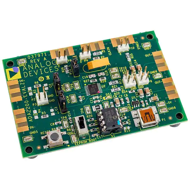
EVALUATION BOARD PHOTOGRAPH
Figure 1.
PLEASE SEE THE LAST PAGE FOR AN IMPORTANT
WARNING AND LEGAL TERMS AND CONDITIONS.
Rev. 0 | Page 1 of 10
�UG-702
ADA2200-EVALZ User Guide
TABLE OF CONTENTS
Evaluation Board Features ............................................................... 1
Output Signal Synchronization ...................................................5
General Description ......................................................................... 1
Programming the ADA2200 ........................................................5
Evaluation Board Photograph ......................................................... 1
Selecting Between I and Q Demodulation Components .........5
Revision History ............................................................................... 2
Default Filter Configuration ........................................................5
Quick Start and Setup Procedure ................................................... 3
Signal Measurements ....................................................................6
Detailed Board Description ............................................................ 4
Evaluation Board Schematic ............................................................8
Synchronous Demodulation Using the ADA2200 ....................... 5
Ordering Information .......................................................................9
Input Signal Synchronization...................................................... 5
Bill of Materials ..............................................................................9
REVISION HISTORY
8/14—Revision 0: Initial Version
Rev. 0 | Page 2 of 10
�ADA2200-EVALZ User Guide
UG-702
QUICK START AND SETUP PROCEDURE
The recommended configuration for initial evaluation is shown
in Figure 2. The signal inputs can handle voltages from 0 V to
3.3 V. Power is supplied through the mini-B USB plug by
connecting it to any powered USB port.
4.
Synchronize the signal generator and the board by
connecting the reference clock output signal (available
through the P9 pins) to a trigger input on the generator.
The signal generation must be configured to start on this
trigger event (burst generation) or to lock to the reference
clock signal (RCK). The detailed configuration depends on
the specific source used.
Connect the signal generator to the IN+ terminal through
the P2 pins and enable the output.
To observe the demodulated signal, probe at P11 and P12.
P11 and P12 are arranged for differential scope probes, but
standard probes or clips work as well. Both the output
synchronization pulse (SYNCO) and RCK can be used to
trigger an oscilloscope.
Observe the filtered output by measuring the voltage
between P7 and P8 with a digital multimeter (DMM).
Set up the ADA2200-EVALZ by completing the following steps:
3.
5.
6.
7.
Table 1. Default Jumper Settings
Designator
P5
P6
P13
Position
1 and 2
2 and 3
2 and 3
Description
IN+ connected to INP
IN− connected to VOCM
On-board clock selected
Pin 1 can be identified by the chamfered corner and number on
the silkscreen.
OSCILLOSCOPE
RCK OUTPUT
P9
50Ω
CLK INPUT
P4
50Ω
P13
TRIG
SYNC OUTPUT
P10
50Ω
1
CH1
CH2
VW
2
CH1 5.00V
FUNCTION
GENERATOR
TRIG
50Ω
IN+
P2
P5
OUT
VOCM
ADA2200
1.58kΩ
P12
50Ω
P6
RESET
I/Q
SEL
M2.00m s
T
3.92000m s
A CH1
3.00V
DMM
20µF
P11
20µF
0V TO 3.0V
IN–
P3
CH2 100m V
OUT+
P7
1.58kΩ
CONFIG
EEPROM
OUT–
P8
USB
(POWER ONLY)
12359-002
2.
Power the board by plugging it into a PC or powered USB
hub. The green LED (DS1) turns on when power is
available.
Verify that the jumper configuration matches the settings
shown in Table 1. With this configuration, the IN+
terminal can be driven with a single-ended source.
Configure a signal generator to source a 6.25 kHz signal.
Offset the output voltage to make sure the signal remains
between 0 V and 3.3 V. An offset at midsupply (1.65 V)
allows maximum signal swing.
Note that many signal generators have a 50 Ω source
impedance and are configured for 50 Ω loads. Therefore,
the voltage swing doubles when the instrument is not
loaded with a 50 Ω impedance. This condition applies to
both the amplitude and offset setting. Verify the actual
signal output with a high input impedance scope before
connecting the signal generator to the ADA2200-EVALZ
board.
00000-000
1.
Figure 2. Suggested Configuration for Quick Start, Showing Connections to Standard Test Equipment
Rev. 0 | Page 3 of 10
�UG-702
ADA2200-EVALZ User Guide
DETAILED BOARD DESCRIPTION
The ADA2200-EVALZ consists of the ADA2200 synchronous
demodulator, powered by the ADP151 3.3 V low dropout
(LDO) regulator. Power is applied through the mini-B USB jack
by connecting the supplied cable to a powered USB port, or by
using the +5V and GND test points adjacent to the USB port.
An on-board oscillator circuit uses a ceramic resonator (ECS,
Inc. ZTB400P [Y1]) to clock the ADA2200 at 400 kHz. This
oscillator circuit centers the band-pass filter at 1/64 of its clock
frequency, or 6.25 kHz. A different clock source and frequency
can be supplied through the CLKIN input, by placing the
jumper P13 between Position 1 and Position 2.
The input signal terminals are labeled IN+ and IN−. By default,
the ADA2200 is configured to be driven by a fully differential
source. The ADA2200 can be driven single-ended by applying
the signal between IN+ and ground, and connecting IN− to
VOCM through the P6 jumper (as shown in Table 1). Note that
the signal range for all the inputs and outputs is 0 V to 3.3 V;
exceeding this range on any input can damage the ADA2200.
There are two output signal terminals on the board. Probing
P11 or P12 with a scope displays the direct output signal from
the ADA2200. The P11 and P12 connectors are arranged to accept
a differential oscilloscope probe, but regular clips can also be
used. Connecting a voltmeter between P7 and P8 allows the
user to measure the dc signal after a 10 Hz, low-pass, RC filter.
The output terminals RCK and SYNCO can be used to
synchronize to the input and output signals, respectively. For
details on how to generate coherent signals or achieve
synchronization, refer to the Input Signal Synchronization
section and Output Signal Synchronization section. A summary
of the signals available on the board is shown on Table 2.
Note that the board includes pads for soldering side, launch,
SMA connectors (see Table 4 and the Johnson 142-0701-851
row). These connectors are commonly available for purchase
from electronic distributors.
Table 2. Terminal Description
Designator
P1
P2
P3
P4
P7
P8
P9
P10
P11
P12
+5V
GNDx
VOCM
TP6
TP7, TP8
TP9
TP10
TP12
Rev. 0 | Page 4 of 10
Signal
+5V
IN+
IN−
CLKIN
OUT+
OUT−
RCK
SYNCO
OUTP
OUTN
+5V
GND
VOCM
BOOT
ISUPPLY
A0
SCL
SDA
Description
Mini-B USB power connector
Noninverting input
Inverting input
External clock input
Noninverted filtered output
Inverted filtered output
Reference clock output
Output synchronization pulse
Noninverted demodulated output
Inverted demodulated output
Mini-B USB power connector
Multiple ground test points
Output common-mode voltage I/O
Boot from EEPROM signal (digital)
10 Ω current shunt for 3.3 V supply
EEPROM address selection
EEPROM clock
EEPROM data
�ADA2200-EVALZ User Guide
UG-702
SYNCHRONOUS DEMODULATION USING THE ADA2200
INPUT SIGNAL SYNCHRONIZATION
PROGRAMMING THE ADA2200
By default, ADA2200 filters and demodulates signals located
exactly at 1/64 of its clock frequency. For example, when using
the 400 kHz on-board oscillator, the demodulated signal
frequency must be 6.25 kHz. Because it is difficult to achieve
coherent, independently generated signals, the clock and the
signal source must be synchronized. This synchronization is
generally accomplished by deriving one signal from the other,
or by employing a phase-locked loop.
The ADA2200 has many programmable features, such as
multiple filter configurations, quadrature demodulation, and
adjustable clock ratios. These features can be programmed via
the serial port interface (SPI) or at power-up when booting
from an I2C EEPROM. For a complete list of features and the
internal register map, refer to the ADA2200 data sheet.
For this purpose, the reference clock signal (RCK) is derived
from the ADA2200 clock, and the default RCK frequency is
fCLK/64. Therefore, if the input signal is synchronized to RCK,
the band-pass filter is automatically centered on the input
signal, and the signal is properly demodulated. In addition,
this configuration allows the system to track any changes in
frequency, because everything is derived from a single master.
Because of these properties, it is possible to use RCK to drive a
signal excitation source, to trigger a pattern generation, or as
the frequency reference in a phase-locked loop generating the
input signal.
OUTPUT SIGNAL SYNCHRONIZATION
An output synchronization pulse is available on the SYNCO
connector. The ADA2200 generates this pulse every time the
output is updated and ready to be sampled. The frequency of
this pulse is 1/8 the clock frequency. By default, the pulse
polarity is positive, and it is generated 6.5 clock cycles after the
last output update.
When the ADA2200 is clocked by the on-board oscillator circuit,
the frequency of the SYNCO pulse is 50 kHz (20 µs period); the
pulse duration is one clock cycle or 2.5 µs (12.5% duty cycle);
and the pulse occurs 16.25 µs after the last output update. The
polarity and its occurrence relative to the output update event
are programmable features.
To program the ADA2200 via the SPI, use the ADA2200SDPEVALZ evaluation board.
SELECTING BETWEEN I AND Q DEMODULATION
COMPONENTS
By default, the ADA2200 performs synchronous demodulation
of the in-phase signal component (I). To demodulate the
quadrature component (Q), set the toggle switch to the
EEPROM_BOOT position and press the RESET button. The
EEPROM contains the same default configuration as the
ADA2200, but sets the quadrature demodulation bit.
The EEPROM must be configured to the factory contents.
Changing the EEPROM contents changes the behavior of the
device after switching the toggle switch.
DEFAULT FILTER CONFIGURATION
The ADA2200 internal filter is configured by default as a
second-order, band-pass filter, as shown in Figure 3.
10
Description
Master clock
Input sampling rate
Input sampling Nyquist rate
Output sampling rate
Output sampling Nyquist rate
Synchronization pulse frequency
Reference clock frequency
Band-pass filter center frequency
Mixer frequency
0
–10
GAIN (dB)
Ratio
1
1
1/2
1/8
1/16
1/8
1/64
1/64
1/64
The internal configuration memory is volatile, and the device
returns to its default value if it does not boot from the EEPROM.
Therefore, it is possible to toggle between the default and the
EEPROM configurations by selecting the appropriate position
of the toggle switch and by then pressing the RESET button.
–20
–30
–40
–50
0.25
0.5
0.75
NORMALIZED FREQUENCY (Hz/Nyquist)
Figure 3. ADA2200 Filter Transfer Function,
Normalized to Half the Output Sampling Rate
Rev. 0 | Page 5 of 10
12359-003
Table 3. Default Clock Frequencies Relative to fCLK
Signal
FCLK
FS
FSN
FD
FDN
FSYNCO
FRCK
FC
FC
On the ADA2200-EVALZ board, the SPI configuration option
is not directly available. The device can be reprogrammed
through the EEPROM option only. A valid configuration must
be loaded on the EEPROM, and the toggle switch must be on
the EEPROM_BOOT position at power up.
�UG-702
ADA2200-EVALZ User Guide
The center frequency of the filter is located at 1/64 of the clock
frequency. As shown in Table 3, this is equivalent to 1/4 of the
Nyquist frequency of the output rate. With the on-board 400 kHz
oscillator, this center frequency is located at 6.25 kHz.
The ADA2200-EVALZ includes a 10 Hz low-pass filter, which
converts the demodulated signal to a dc voltage level. This
conversion makes it possible to use a simple voltmeter to
perform amplitude and phase measurements.
The filter transfer function scales with the input clock frequency.
Valid input clock frequencies range from 10 kHz to 1 MHz.
Sweeping the input clock frequency in this range sweeps the
filter center frequency from 156.25 Hz to 15.625 kHz. The filter
Q remains constant at 1.7 for any CLKIN frequency.
Amplitude Measurements
Connect Pin 1 and Pin 2 on P13 to use an external clock with
the device.
The relationship between the signal amplitude and the output
level depends on the relative phase between RCLK and the
signal. This relationship is analogous to measuring the
amplitude of a signal by looking at its crest (maximum
amplitude point) or zero crossing. When the signal amplitude
changes, the voltage at the crest sees the greatest change. In
contrast, the zero crossing remains at zero. Because these two
points are 90 degrees from each other, they are in quadrature.
Programming Different Filter Configurations
If the desired filter is different from the default definition, the
ADA2200 must boot from an EEPROM previously programmed
with valid contents for all the user registers. For additional details
on how to boot from EEPROM, refer to the Programming the
ADA2200 section.
For information on programming the EEPROM with a different
filter function, contact technical support.
SIGNAL MEASUREMENTS
The signal present at the output of the ADA2200 depends on
the amplitude and phase (relative to the reference clock) of the
signal applied at its inputs. When either the amplitude or phase
is known and constant, any output variations can be attributed
to the modulated parameter.
This dependence is shown in Figure 4. In any of these cases,
the ADA2200 is performing either amplitude or phase
demodulation.
ΔA1
θ1
0
90
ΔA2
θ2
180
270
0
90
PHASE (degrees)
180
270
0
12359-004
AMPLITUDE (V)
Δθ
ΔA2
0
If the relative phase of the signal makes the amplitude
measurement too small to measure, toggle the switch labeled
EEPROM_BOOT and press the RESET button. This action
allows the ADA2200 to boot with the EEPROM contents, which
are the same as the default configuration, except that the
ADA2200 demodulates the quadrature component instead.
Phase Measurements
If the amplitude of the signal present at the inputs of ADA2200
remains constant, the output varies as a function of the relative
phase between the signal and the reference clock (RCLK).
As long as the phase shifts are small, this relationship is
approximately linear; however, the gain (slope) of this
relationship depends on the relative phase shift between the
signal and RCLK. For example, if the phase shift occurs around
the crest of the signal, the change at the output is barely
noticeable. In addition, the user is not able to distinguish
between a positive and a negative shift. In contrast, the
maximum phase sensitivity is achieved when the phase shift
happens around the zero crossing. Because these two points are
90° from each other, they are in quadrature.
Δθ
ΔA1
If the phase of the signal present at the inputs of ADA2200
remains constant, the output behaves as a linear function of the
signal amplitude. In other words, if the amplitude of the signal
doubles, the output voltage also doubles.
Figure 4. Measurement Dependence on Phase and Amplitude Variations
If the relative phase of the signal makes the phase measurement
too small to measure, toggle the EEPROM_BOOT switch and
press the RESET button. This combination allows the ADA2200
to boot with the EEPROM contents, which are the same as the
default configuration, except that the ADA2200 demodulates
the quadrature component instead.
Rev. 0 | Page 6 of 10
�ADA2200-EVALZ User Guide
UG-702
Amplitude and Phase Measurements
When the amplitude and phase are unknown, it is necessary to
obtain two orthogonal components of the signal to determine
its amplitude, phase, or both. These two components are in
phase and in quadrature relative to each other; the popular
nomenclature used for these component is I and Q.
A signal with two known rectangular components can be
represented as a phase vector or phasor with an associated
amplitude and phase. This representation is show in Figure 5.
II
A = I 2 + Q2
θ = sin−1(Q/A)
Or, alternatively:
θ = cos−1(I/A)
The inverse sine or inverse cosine functions involving the I and Q
components linearize the relationship between the phase of the
signal and the measured angle. This calculation also makes it
possible to separate the effects of amplitude and phase variations.
I
A
Q
θ
Because the inverse sine and inverse cosine are only defined in
two quadrants, the sign of the I and Q components must be
taken into account to map the result to cover the entire 360°.
IV
12359-005
I
III
this switching is accomplished by toggling the EEPROM_BOOT
switch and pressing the RESET button. The dc voltage at the
output represents the I and Q components. Perform the
following calculations to find the amplitude and phase:
Figure 5. Signal Represented as Phasor
If the signal amplitude and phase are relatively constant for the
duration of the measurement, it is possible to switch the ADA2200
to return the I and Q components. On the ADA2200-EVALZ,
It is not recommended to use the inverse tangent function to
extract the phase information, because the function is not defined
at +90° and −90°. This function causes the phase measurement
to become very sensitive to measurement errors and noise.
Rev. 0 | Page 7 of 10
�UG-702
ADA2200-EVALZ User Guide
EVALUATION BOARD SCHEMATIC
+5V
1
2
3
600OHM
C1
10µF
G1
G2
G3
G4
C4
1µF
VIN
EN
NC
U1
4
VOUT
3V3
5
GND
2
C6
0.1µF
C9
10µF
C7
1µF
100Ω
NC001
NC002
A
GND
PINS
ADP151AUJZ-3.3-R7
E1
1
1
2
3
4
5
R10
1
P1
GND8
DS1
TP7
KELVIN
CONNECTION 1
1
C
1
SML-310MTT86
TP8
R17
10Ω
P2
2
1
P3
1
3
2
1
R5
C3
R4
DNP
0Ω
2 3 4 5
TBD0805
IN–
C5
1µF
P11
VDD
OUTP
OUTN
5
11
10
3
A0
14 SDA
15 SCL
2
16
R9
N3 3
N4 4
100Ω
C8
0.33µF
FSM2JSMA
10µF
5 4 3 2
10µF
P7
1
2
LAYOUT AS
2 × 2 – 0.1IN
PATTERN
TP9
TP12
2
1
TP10
ADA2200
LAYOUT AS
2 × 2 – 0.1IN
PATTERN
2
1
P12
P8
OUT–
R22
R24
49.9Ω
1.58kΩ
R27
3
2
1
P13
RESET
FC=10HZ
1
2
P6
1 N1
2 N2
1
1.58kΩ
12
CS/A0
RST 9
RST
SDIO/SDA
BOOT 4
SCK/SCL
13 BOOT
SYNCO
RCLK/SDO
1
XOUT
CLKIN
GND
1
VOCM
5015
OUT+
R23
C13
U2
6
INP
7
INN
8
VOCM
1
2
LAYOUT AS
2 × 2 – 0.1IN
PATTERN
R21
49.9Ω
C14
1
2
3
1
C12
C2
TBD0805
R3
2 3 4 5
DNP
0
C11
1µF
FC = 10Hz
10µF
C15
P5
R6
IN+
1
C10
0.1µF
5 4 3 2
10µF
1MΩ
DNI
1
2
R28
470Ω
Y1
C18
120pF
C19
470pF
SYNCO
R25
1
3.3V
3
1
P10 49.9Ω
TP6
5015
EEPROM_BOOT
1
1
2
R8
2
100Ω
5 4 3 2
69157-102
C16
0.01µF
OS102011MS2QN1
R2
R26
1
2
P4
1
2
RCK
1
49.9Ω
P9
49.9Ω
5 4 3 2
69157-102
3.3V
R14
10kΩ
10kΩ
R20
10kΩ
R19
R18
DNI
10kΩ
A0
A1
10kΩ
R16
C17
R15
69157-102
0.1µF
2 3 4 5
R1
0Ω
GND1 GND2 GND3
1
X1
1
2
3
4
1
2
3
4
8
7
6
5
8
7
6
5
1
1
GND4 GND5 GND6 GND7
1
1
1
1
SCL
SDA
110-43-308-41-001000
DIP-8 EEPROM SOCKET
EEPROM TO BE INSTALLED:
AT24C02C-PUM
(8-LEAD PDIP OR EQUIVALENT)
Figure 6. ADA2200-EVALZ Schematic
Rev. 0 | Page 8 of 10
12359-006
1 CLKIN
�ADA2200-EVALZ User Guide
UG-702
ORDERING INFORMATION
BILL OF MATERIALS
Table 4.
Qty.
16
6
4
3
1
1
1
1
1
1
1
1
9
3
5
3
5
1
3
1
1
1
1
1
1
1
4
2
1
7
2
2
1
Designator
+5 V, TP6 to TP10, GND1
to GND8, TP12, VOCM
C1, C9, C12 to C15
C4, C5, C7, C11
C6, C10, C17
C16
C18
C19
C8
DS1
E1
EEPROM_BOOT
P1
P2 to P4,P7 to P12
P5, P6, P13
R1, R21, R22, R25, R26
R8 to R10
R14, R16, R18 to R20
R17
R2, R5, R6
R27
R28
RESET
U1
U2
X1
Y1
Corners
R23, R24
Y1
IN+, IN−, RCK, OUT+,
OUT−, CLKIN, SYNCO
C2, C3
R3, R4
R15
Description
Conn, printed circuit board (PCB) SMT test points
Capacitor, ceramic, monolithic, X5R, 25 V
Capacitor, ceramic, monolithic, X5R, 25 V
Capacitor, ceramic, X7R, 0603, 50 V
Capacitor, ceramic, chip, C0G, 0603, 25 V
Capacitor, ceramic, NP0, 0805, 50 V
Capacitor, ceramic, NP0, 50 V
Capacitor, ceramic, X5R, 16 V
LED, green, surface mount
Inductor chip ferrite bead
Switch, SPDT, PCB mounted slide
Conn, PCB USB mini-B, receptacle ASSY SMT
Conn, PCB Berg jumper, ST, male, 2-pin
Conn, PCB Berg header, ST, male, 3-pin
Resistor, precision thick film chip, R1206
Resistor, precision thick film chip, R0603
Resistor, precision thick film chip, R0603
Resistor, antisurge thick film chip
Resistor, thick film chip
Resistor, precision thick film chip, R0805
Resistor, metal film chip, 0.1%
Switch, tactile, SPST NO
IC, CMOS linear regulator, LDO, 3.3 V
IC, sampled analog filter, synchronous demodulator
Socket, 8-pin, DIP
Ceramic resonator, 400 kHz
Bump on, cylindrical, 0.312X.200, black
Resistor, precision thin film chip, R0603
IC, EEPROM, 2 kb, 1 MHz, 8-DIP
Conn, PCB, coaxial, SMA end launch (not installed)
Manufacturer
Keystone Electronics
Corp.
Murata
Murata
AVX
Kemet
AVX
Phycomp (Yageo)
AVX
ROHM
Murata
ITT
Molex
Berg
Samtec
Panasonic
Multicomp
Panasonic
Panasonic
Panasonic
Panasonic
Panasonic
TE Connectivity
Analog Devices
Analog Devices
Mill-Max
ECS
3M
Panasonic
ATMEL
Johnson
GRM31CR61E106KA12L
GRM188R61E105KA12D
06035C104KAT2A
C0603C103J3GACTU
08055A121JAT2A
2238 861 15471
0603YD334KAT2A
SML-310MTT86
BLM15AX601SN1D
OS102011MS2QN1
54819-0572
69157-102
TSW-103-08-G-S
ERJ-8ENF49R9V
MC 0.063 W, 0603, 1%, 100 Ω
ERJ-3EKF1002V
ERJP14F10R0U
ERJ-6GEY0R00V
ERJ-6ENF1004V
ERA-6AEB471V
FSM2JSMA
ADP151AUJZ-3.3-R7
ADA2200
110-43-308-41-001000
ZTB400P
SJ61A1
ERA-3AEB1581V
AT24C02C-PUM
142-0701-851
Not installed (TBD_C0805)
Not installed (TBD_R1206)
Not installed (TBD_R0603)
TBD0805
Panasonic
Panasonic
TBD0805
ERJ-8ENF49R9V
ERJ-3EKF1002V
Rev. 0 | Page 9 of 10
Part No.
5015
�UG-702
ADA2200-EVALZ User Guide
NOTES
I2C refers to a communications protocol originally developed by Philips Semiconductors (now NXP Semiconductors).
ESD Caution
ESD (electrostatic discharge) sensitive device. Charged devices and circuit boards can discharge without detection. Although this product features patented or proprietary protection
circuitry, damage may occur on devices subjected to high energy ESD. Therefore, proper ESD precautions should be taken to avoid performance degradation or loss of functionality.
Legal Terms and Conditions
By using the evaluation board discussed herein (together with any tools, components documentation or support materials, the “Evaluation Board”), you are agreeing to be bound by the terms and conditions
set forth below (“Agreement”) unless you have purchased the Evaluation Board, in which case the Analog Devices Standard Terms and Conditions of Sale shall govern. Do not use the Evaluation Board until you
have read and agreed to the Agreement. Your use of the Evaluation Board shall signify your acceptance of the Agreement. This Agreement is made by and between you (“Customer”) and Analog Devices, Inc.
(“ADI”), with its principal place of business at One Technology Way, Norwood, MA 02062, USA. Subject to the terms and conditions of the Agreement, ADI hereby grants to Customer a free, limited, personal,
temporary, non-exclusive, non-sublicensable, non-transferable license to use the Evaluation Board FOR EVALUATION PURPOSES ONLY. Customer understands and agrees that the Evaluation Board is provided
for the sole and exclusive purpose referenced above, and agrees not to use the Evaluation Board for any other purpose. Furthermore, the license granted is expressly made subject to the following additional
limitations: Customer shall not (i) rent, lease, display, sell, transfer, assign, sublicense, or distribute the Evaluation Board; and (ii) permit any Third Party to access the Evaluation Board. As used herein, the term
“Third Party” includes any entity other than ADI, Customer, their employees, affiliates and in-house consultants. The Evaluation Board is NOT sold to Customer; all rights not expressly granted herein, including
ownership of the Evaluation Board, are reserved by ADI. CONFIDENTIALITY. This Agreement and the Evaluation Board shall all be considered the confidential and proprietary information of ADI. Customer may
not disclose or transfer any portion of the Evaluation Board to any other party for any reason. Upon discontinuation of use of the Evaluation Board or termination of this Agreement, Customer agrees to
promptly return the Evaluation Board to ADI. ADDITIONAL RESTRICTIONS. Customer may not disassemble, decompile or reverse engineer chips on the Evaluation Board. Customer shall inform ADI of any
occurred damages or any modifications or alterations it makes to the Evaluation Board, including but not limited to soldering or any other activity that affects the material content of the Evaluation Board.
Modifications to the Evaluation Board must comply with applicable law, including but not limited to the RoHS Directive. TERMINATION. ADI may terminate this Agreement at any time upon giving written notice
to Customer. Customer agrees to return to ADI the Evaluation Board at that time. LIMITATION OF LIABILITY. THE EVALUATION BOARD PROVIDED HEREUNDER IS PROVIDED “AS IS” AND ADI MAKES NO
WARRANTIES OR REPRESENTATIONS OF ANY KIND WITH RESPECT TO IT. ADI SPECIFICALLY DISCLAIMS ANY REPRESENTATIONS, ENDORSEMENTS, GUARANTEES, OR WARRANTIES, EXPRESS OR IMPLIED, RELATED
TO THE EVALUATION BOARD INCLUDING, BUT NOT LIMITED TO, THE IMPLIED WARRANTY OF MERCHANTABILITY, TITLE, FITNESS FOR A PARTICULAR PURPOSE OR NONINFRINGEMENT OF INTELLECTUAL
PROPERTY RIGHTS. IN NO EVENT WILL ADI AND ITS LICENSORS BE LIABLE FOR ANY INCIDENTAL, SPECIAL, INDIRECT, OR CONSEQUENTIAL DAMAGES RESULTING FROM CUSTOMER’S POSSESSION OR USE OF
THE EVALUATION BOARD, INCLUDING BUT NOT LIMITED TO LOST PROFITS, DELAY COSTS, LABOR COSTS OR LOSS OF GOODWILL. ADI’S TOTAL LIABILITY FROM ANY AND ALL CAUSES SHALL BE LIMITED TO THE
AMOUNT OF ONE HUNDRED US DOLLARS ($100.00). EXPORT. Customer agrees that it will not directly or indirectly export the Evaluation Board to another country, and that it will comply with all applicable
United States federal laws and regulations relating to exports. GOVERNING LAW. This Agreement shall be governed by and construed in accordance with the substantive laws of the Commonwealth of
Massachusetts (excluding conflict of law rules). Any legal action regarding this Agreement will be heard in the state or federal courts having jurisdiction in Suffolk County, Massachusetts, and Customer hereby
submits to the personal jurisdiction and venue of such courts. The United Nations Convention on Contracts for the International Sale of Goods shall not apply to this Agreement and is expressly disclaimed.
©2014 Analog Devices, Inc. All rights reserved. Trademarks and
registered trademarks are the property of their respective owners.
UG12359-0-8/14(0)
Rev. 0 | Page 10 of 10
�