Low Cost, Dual, High Current Output Line Driver with Shutdown ADA4310-1
FEATURES
High speed −3 dB bandwidth: 190 MHz, G = +5 Slew rate: 820 V/μs, RLOAD = 50 Ω Wide output swing 20.4 V p-p differential, RLOAD of 100 Ω from 12 V supply High output current Low distortion −95 dBc typical at 1 MHz, VOUT = 2 V p-p, G = +5, RLOAD = 50 Ω −69 dBc typical at 10 MHz, VOUT = 2 V p-p, G = +5, RLOAD = 50 Ω Power management and shutdown Control inputs CMOS level compatible Shutdown quiescent current 0.65 mA/amplifier Adjustable low quiescent current: 3.9 mA to 7.6 mA per amp
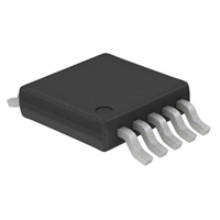
PIN CONFIGURATIONS
+VS 1 NC 2 OUT A 3 –IN A 4 +IN A 5
10 9 8 7 6
OUT B –IN B +IN B PD1
06027-001
PD0
NC = NO CONNECT
Figure 1. Thermally Enhanced, 10-Lead MINI_SO_EP
16 OUT A
15 NC
13 OUT B
14 +VS
NC 1 −IN A 2 +IN A 3 GND 4 NC = NO CONNECT
12 NC 11 −IN B 10 +IN B 9 PD1
APPLICATIONS
Home networking line drivers Twisted pair line drivers Power line communications Video line drivers ARB line drivers I/Q channel amplifiers
PD0 8
–VS 7
NC 5
NC 6
Figure 2. Thermally Enhanced, 4 mm × 4 mm 16-Lead LFCSP_VQ
GENERAL DESCRIPTION
The ADA4310-1 is comprised of two high speed, current feedback operational amplifiers. The high output current, high bandwidth, and fast slew rate make it an excellent choice for broadband applications requiring high linearity performance while driving low impedance loads. The ADA4310-1 incorporates a power management function that provides shutdown capabilities and/or the ability to optimize the amplifiers quiescent current. The CMOScompatible, power-down control pins (PD1 and PD0) enable the ADA4310-1 to operate in four different modes: full power, medium power, low power, and complete power down. In the power-down mode, quiescent current drops to only 0.65 mA/amplifier, while the amplifier output goes to a high impedance state. The ADA4310-1 is available in a thermally enhanced, 10-lead MSOP with an exposed paddle for improved thermal conduction and in a thermally enhanced, 4 mm × 4 mm 16-lead LFCSP. The ADA4310-1 is rated to work in the extended industrial temperature range of −40°C to +85°C.
1/2
ADA4310-1
VMID1
1/2
06027-003
ADA4310-1
VCC – VEE 1V = MID 2
Figure 3. Typical PLC Driver Application
Rev. 0
Information furnished by Analog Devices is believed to be accurate and reliable. However, no responsibility is assumed by Analog Devices for its use, nor for any infringements of patents or other rights of third parties that may result from its use. Specifications subject to change without notice. No license is granted by implication or otherwise under any patent or patent rights of Analog Devices. Trademarks and registered trademarks are the property of their respective owners.
One Technology Way, P.O. Box 9106, Norwood, MA 02062-9106, U.S.A. Tel: 781.329.4700 www.analog.com Fax: 781.461.3113 ©2006 Analog Devices, Inc. All rights reserved.
06027-002
�ADA4310-1 TABLE OF CONTENTS
Features .............................................................................................. 1 Applications....................................................................................... 1 Pin Configurations ........................................................................... 1 General Description ......................................................................... 1 Revision History ............................................................................... 2 Specifications..................................................................................... 3 Absolute Maximum Ratings............................................................ 5 Thermal Resistance ...................................................................... 5 ESD Caution.................................................................................. 5 Pin Configurations and Function Descriptions ........................... 6 Typical Performance Characteristics ............................................. 7 Theory of Operation ...................................................................... 10 Application Information................................................................ 11 Feedback Resistor Selection...................................................... 11 Power Control Modes of Operation ........................................ 11 Exposed Thermal Pad Connections ........................................ 11 Power Line Application ............................................................. 11 Board Layout............................................................................... 12 Power Supply Bypassing ............................................................ 12 Outline Dimensions ....................................................................... 13 Ordering Guide .......................................................................... 13
REVISION HISTORY
10/06—Revision 0: Initial Version
Rev. 0 | Page 2 of 16
�ADA4310-1 SPECIFICATIONS
VS = 12 V, ±6 V (@ TA = 25°C, G = +5, RL = 100 Ω, unless otherwise noted). Table 1.
Parameter DYNAMIC PERFORMANCE −3 dB Bandwidth Test Conditions/Comments G = +5, VOUT = 0.1 V p-p, PD1 = 0, PD0 = 0 PD1 = 0, PD0 = 1 PD1 = 1, PD0 = 0 G = +5, VOUT = 2 V p-p, RLOAD = 50 Ω, PD1 = 0, PD0 = 0 PD1 = 0, PD0 = 1 PD1 = 1, PD0 = 0 fC = 1 MHz, VOUT = 2 V p-p, RLOAD = 50 Ω PD1 = 0, PD0 = 0 PD1 = 0, PD0 = 1 PD1 = 1, PD0 = 0 fC = 10 MHz, VOUT = 2 V p-p, RLOAD = 50 Ω PD1 = 0, PD0 = 0 PD1 = 0, PD0 = 1 PD1 = 1, PD0 = 0 fC = 20 MHz, VOUT = 2 V p-p, RLOAD = 50 Ω PD1 = 0, PD0 = 0 PD1 = 0, PD0 = 1 PD1 = 1, PD0 = 0 f = 100 kHz f = 100 kHz Min Typ 190 140 100 820 790 750 Max Unit MHz MHz MHz V/μs V/μs V/μs
Slew Rate
NOISE/DISTORTION PERFORMANCE Distortion (Worst Harmonic)
−95 −88 −77 −69 −57 −47 −50 −42 −35 2.85 21.8 1 −2 6
dBc dBc dBc dBc dBc dBc dBc dBc dBc nV/√Hz pA/√Hz mV μA μA MΩ MΩ dB kΩ VP VP VP VP V p-p ±6 +12 V V mA/amp mA/amp mA/amp mA/amp
Input Voltage Noise Input Current Noise DC PERFORMANCE Input Offset Voltage Input Bias Current Noninverting Input Inverting Input Open-Loop Transimpedance
RLOAD = 50 Ω RLOAD = 100 Ω Common-Mode Rejection INPUT CHARACTERISTICS Input Resistance OUTPUT CHARACTERISTICS Single-Ended +Swing Single-Ended −Swing Single-Ended +Swing Single-Ended −Swing Differential Swing POWER SUPPLY Operating Range (Dual Supply) Operating Range (Single Supply) Supply Current
14 35 −62 500 +5.08 −5.12 +5.14 −5.17 20.4 ±2.5 +5
f < 100 kHz RLOAD = 50 Ω RLOAD = 50 Ω RLOAD = 100 Ω RLOAD = 100 Ω RLOAD = 100 Ω
PD1 = 0, PD0 = 0 PD1 = 0, PD0 = 1 PD1 = 1, PD0 = 0 PD1 = 1, PD0 = 1
7.6 5.6 3.9 0.65
Rev. 0 | Page 3 of 16
�ADA4310-1
Parameter POWER DOWN PINS PD1, PD0 Threshold PD1, PD0 = 0 Pin Bias Current PD1, PD0 = 1 Pin Bias Current Enable/Disable Time Power Supply Rejection Ratio Test Conditions/Comments Referenced to GND PD1 or PD0 = 0 V PD1 or PD0 = 3 V Positive/Negative Min Typ 1.5 −0.2 70 0.04/2 −70/−60 Max Unit V μA μA μs dB
Rev. 0 | Page 4 of 16
�ADA4310-1 ABSOLUTE MAXIMUM RATINGS
Table 2.
Parameter Supply Voltage 10-Lead MINI_SO_EP 16-Lead LFCSP_VQ Power Dissipation Storage Temperature Range Operating Temperature Range Lead Temperature (Soldering 10 sec) Junction Temperature Rating 12 V ±6V ( TJMAX − TA)/θJA −65°C to +125°C −40°C to +85°C 300°C 150°C
Maximum Power Dissipation
The maximum safe power dissipation for the ADA4310-1 is limited by the associated rise in junction temperature (TJ) on the die. At approximately 150°C, which is the glass transition temperature, the plastic changes its properties. Even temporarily exceeding this temperature limit can change the stresses that the package exerts on the die, permanently shifting the parametric performance of the amplifiers. Exceeding a junction temperature of 150°C for an extended period can result in changes in silicon devices, potentially causing degradation or loss of functionality. Figure 4 shows the maximum safe power dissipation in the package vs. the ambient temperature for the 10-lead MINI_SO_EP (44°C/W) and for the 16-lead LFCSP_VQ (63°C/W) on a JEDEC standard 4-layer board. θJA values are approximations.
5.0 4.5
Stresses above those listed under Absolute Maximum Ratings may cause permanent damage to the device. This is a stress rating only; functional operation of the device at these or any other conditions above those indicated in the operational section of this specification is not implied. Exposure to absolute maximum rating conditions for extended periods may affect device reliability.
MAXIMUM POWER DISSIPATION (W)
THERMAL RESISTANCE
θJA is specified for the worst-case conditions, that is, θJA is specified for device soldered in circuit board for surface-mount packages. Table 3.
Package Type 10-Lead MINI_SO_EP 16-Lead LFCSP_VQ θJA 44 63 Unit °C/W °C/W
4.0 3.5 3.0 2.5 LFCSP_VQ-16 2.0 1.5 1.0 0.5 –35 –15 5 25 45 65 85
06027-016
MINI_SO_EP-10
0
AMBIENT TEMPERATURE (°C)
Figure 4. Maximum Power Dissipation vs. Temperature for a 4-Layer Board
ESD CAUTION
ESD (electrostatic discharge) sensitive device. Electrostatic charges as high as 4000 V readily accumulate on the human body and test equipment and can discharge without detection. Although this product features proprietary ESD protection circuitry, permanent damage may occur on devices subjected to high energy electrostatic discharges. Therefore, proper ESD precautions are recommended to avoid performance degradation or loss of functionality.
Rev. 0 | Page 5 of 16
�ADA4310-1 PIN CONFIGURATIONS AND FUNCTION DESCRIPTIONS
16 OUT A 15 NC 14 +VS 13 OUT B
+VS 1 NC 2 OUT A 3 –IN A 4 +IN A 5
10 9 8 7 6
OUT B –IN B +IN B PD1
06027-001
NC 1 −IN A 2 +IN A 3 GND 4 NC = NO CONNECT
12 NC 11 −IN B 10 +IN B 9 PD1
PD0 8
–VS 7
NC 5
NC 6
NC = NO CONNECT
Figure 5. 10-Lead MSOP Pin Configuration
Figure 6. 16-Lead LFCSP Pin Configuration
Table 4. 10-Lead MSOP Pin Function Description
Pin No. 1 2 3 4 5 6 7 8 9 10 11 (Exposed Paddle) Mnemonic +VS NC OUT A −IN A +IN A PD0 PD1 +IN B −IN B OUT B GND Description Positive Power Supply Input No Connection Amplifier A Output Amplifier A Inverting Input Amplifier A Noninverting Input Power Dissipation Control Power Dissipation Control Amplifier B Noninverting Input Amplifier B Inverting Input Amplifier B Output Ground (Electrical Connection Required)
Table 5. 16-Lead LFCSP Pin Function Description
Pin No. 1, 5, 6, 12, 15 2 3 4 7 8 9 10 11 13 14 16 17 (Exposed Paddle) Mnemonic NC −IN A +IN A GND −VS PD0 PD1 +IN B −IN B OUT B +VS OUT A GND Description No Connection Amplifier A Inverting Input Amplifier A Noninverting Input Ground Negative Power Supply Input Power Dissipation Control Power Dissipation Control Amplifier B Noninverting Input Amplifier B Inverting Input Amplifier B Output Positive Power Supply Input Amplifier A Output Ground
Rev. 0 | Page 6 of 16
06027-002
PD0
�ADA4310-1 TYPICAL PERFORMANCE CHARACTERISTICS
12 9 6
NORMALIZED GAIN (dB)
VOUT = 100mV p-p RL = 50Ω PD1, PD0 = 0, 0
–20
G = +2
HARMONIC DISTORTION (dBc)
–30 –40 –50 –60 –70 –80 –90 –100 –110
06027-022
VOUT = 2V p-p RL = 50Ω G = +5 PD1, PD0 = 1, 0 PD1, PD0 = 0, 1 PD1, PD0 = 0, 0
HD2 HD3
3 0 –3 –6 –9 –12 –15 –18 1 10 100 1000 G = +20 G = +10 G = +5
1
10 FREQUENCY (MHz)
100
FREQUENCY (MHz)
Figure 7. Small Signal Frequency Response for Various Closed-Loop Gains
23 20 17 14 11
Figure 10. Harmonic Distortion vs. Frequency
100
VOUT = 100mV p-p G = +5 RL = 50Ω
PD1, PD0 = 0, 0
8 5 2 –1 –4 –7
PD1, PD0 = 0, 1
VOLTAGE NOISE (nV/√Hz)
GAIN (dB)
10
PD1, PD0 = 1, 0
FREQUENCY (MHz)
FREQUENCY (Hz)
Figure 8. Small Signal Frequency Response for Various Modes
100000 0°
Figure 11. Voltage Noise vs. Frequency
0.20 0.15 0.10
RL = 100Ω
10000
–45
G = +5 RL = 50Ω 10ns/DIV
MAGNITUDE (kΩ)
PHASE (Degrees)
1000
–90
100
–135
OUTPUT (V)
0.05 0 –0.05 –0.10
10
–180
1
–225
06027-020
–0.15
0.1 0.0001 –270 1000
0.001
0.01
0.1
1
10
100
FREQUENCY (MHz)
Figure 9. Open-Loop Transimpedance Gain and Phase vs. Frequency
06027-013
–0.20
Figure 12. Small Signal Transient Response
Rev. 0 | Page 7 of 16
06027-012
10
100
1000
06027-021
–10
1
1
10
100
1k
10k
100k
1M
10M
100M
1G
06027-023
–120 0.1
�ADA4310-1
0 –10 –20 –30 –40 –50 –60 –70 0.01
–120 –60
PD1, PD0 = (0, 0) RL = 100Ω
–40
PD1, PD0 = (1,1)
COMMON-MODE REJECTION (dB)
FEEDTHROUGH (dB)
06027-007
–80
–100
0.1
1
10
100
1000
1
10
100
1000
FREQUENCY (MHz)
FREQUENCY (MHz)
Figure 13. Common-Mode Rejection(CMR) vs. Frequency
0 –10
POWER SUPPLY REJECTION (dB)
Figure 16. Off-Isolation vs. Frequency
1000
G = +5 PD1, PD0 = (0, 0) RL = 100Ω
PD1, PD0 = (1,1)
100
OUTPUT IMPEDANCE (kΩ)
–20 –30 –40 –PSR –50 –60 –70 –80 0.01
10
+PSR
1
0.1
0.01
0.1
1
10
100
1000
FREQUENCY (MHz)
FREQUENCY (MHz)
Figure 14. Power Supply Rejection(PSR) vs. Frequency
100
Figure 17. Output Impedance vs. Frequency (Disabled)
2.5
PD1, PD0 = (0, 0)
10ns/DIV VOUT
2.0
OUTPUT IMPEDANCE (Ω)
10
1.5
1
VPD0, VPD1
VOLTAGE (V)
1.0
0.1
0.5
0
1 10 FREQUENCY (MHz) 100 1000
06027-009
06027-008
0.1
1
10
100
1000
06027-006
0.001 0.01
06027-010
0.01 0.1
–0.5
Figure 15. Closed-Loop Output Impedance vs. Frequency
Figure 18. Power-Down Turn On/Turn Off
Rev. 0 | Page 8 of 16
06027-011
�ADA4310-1
0
–20
CROSSTALK (dB)
–40
–60
–80
–100
1
10 FREQUENCY (MHz)
100
1000
Figure 19. Crosstalk
06027-014
–120 0.1
Rev. 0 | Page 9 of 16
�ADA4310-1 THEORY OF OPERATION
The ADA4310-1 is a current feedback amplifier with high output current capability. With a current feedback amplifier, the current into the inverting input is the feedback signal, and the open-loop behavior is that of a transimpedance, dVO/dIIN or TZ. The open-loop transimpedance is analogous to the open-loop voltage gain of a voltage feedback amplifier. Figure 20 shows a simplified model of a current feedback amplifier. Because RIN is proportional to 1/gm, the equivalent voltage gain is just TZ × gm, where gm is the transconductance of the input stage. Basic analysis of the follower with gain circuit yields
VO TZ ( s ) = G× VIN TZ ( s ) + G × RIN + RF
Because G × RIN