Wideband, Differential, High Output Current
Line Driver with Shutdown
ADA4312-1
Data Sheet
13 OUT B
15 NC
14 VCC
16 OUT A
FUNCTIONAL BLOCK DIAGRAM
NC 1
12 NC
–IN A 2
ADA4312-1
10 +IN B
9 SD
NC = NO CONNECT. DO NOT CONNECT
TO THIS PIN.
11044-001
NC 8
GND 4
11 –IN B
VEE 7
+IN A 3
NC 6
High speed
−3 dB bandwidth: 195 MHz, GDIFF = +16 V/V, RL, DIFF = 40 Ω
Differential slew rate: 2100 V/µs
Wide output swing: 18.0 V p-p differential, 12 V supply
High output current: 225 mA peak
G.hn MTPR at 16 dBm line power
−64 dBc typical at 5 MHz, referred to −58 dBm/Hz
−64 dBc typical at 17 MHz, referred to −58 dBm/Hz
−64 dBc typical at 28 MHz, referred to −58 dBm/Hz
−63 dBc typical at 31 MHz, referred to −58 dBm/Hz
−61 dBc typical at 59 MHz, referred to −58 dBm/Hz
−62 dBc typical at 82 MHz, referred to −58 dBm/Hz
Shutdown
CMOS-compatible SD pin
Shutdown quiescent current: 3 mA
ZOUT in shutdown: 10 kΩ differential (open-loop)
Resistor adjustable quiescent current
IADJ 5
FEATURES
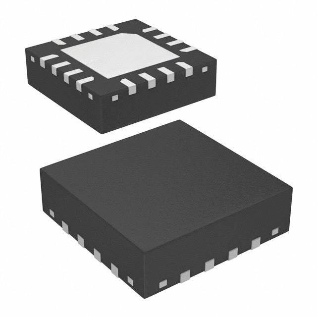
Figure 1. Thermally Enhanced, 4 mm × 4 mm, 16-Lead LFCSP
TYPICAL APPLICATION CIRCUIT
1/2
APPLICATIONS
ADA4312-1
ITU G.hn (ITU G.9960/G.9961)
HomePlug AV
HomePlug AV2
IEEE 1901
VMID*
The ADA4312-1 is a high speed, differential, current feedback line
driver designed for half-duplex G.hn power line communication
(PLC) modems. The high output current, high bandwidth, and
slew rate of 2100 V/µs make the ADA4312-1 an excellent choice
for G.hn broadband applications that require high linearity
while driving low impedance loads.
VMID =
VCC
2
ADA4312-1
11044-002
1/2
GENERAL DESCRIPTION
Figure 2. Typical PLC Driver Application
The CMOS-compatible shutdown control pin (SD) reduces
the quiescent current to 3 mA while maintaining an output
impedance of 10 kΩ differential. The ADA4312-1 also provides
resistor adjustable quiescent current for improved efficiency in
transmit mode.
The ADA4312-1 is available in a thermally enhanced, 16-lead
LFCSP with an exposed pad to facilitate robust thermal
management. The ADA4312-1 is rated to operate over the
extended industrial temperature range of −40°C to +85°C.
Rev. A
Document Feedback
Information furnished by Analog Devices is believed to be accurate and reliable. However, no
responsibility is assumed by Analog Devices for its use, nor for any infringements of patents or other
rights of third parties that may result from its use. Specifications subject to change without notice. No
license is granted by implication or otherwise under any patent or patent rights of Analog Devices.
Trademarks and registered trademarks are the property of their respective owners.
One Technology Way, P.O. Box 9106, Norwood, MA 02062-9106, U.S.A.
Tel: 781.329.4700 ©2012–2017 Analog Devices, Inc. All rights reserved.
Technical Support
www.analog.com
�ADA4312-1
Data Sheet
TABLE OF CONTENTS
Features .............................................................................................. 1
Test Circuit .........................................................................................8
Applications ....................................................................................... 1
Applications Information .................................................................9
General Description ......................................................................... 1
Feedback Resistor Selection .........................................................9
Functional Block Diagram .............................................................. 1
General Operation ........................................................................9
Typical Application Circuit ............................................................. 1
Half-Duplex Operation ................................................................9
Revision History ............................................................................... 2
Establishing VMID ...........................................................................9
Specifications..................................................................................... 3
Bias Control and Linearity ...........................................................9
Absolute Maximum Ratings ............................................................ 4
PCB Layout ................................................................................. 10
Thermal Resistance ...................................................................... 4
Thermal Management ............................................................... 10
Maximum Power Dissipation ..................................................... 4
Power Supply Bypassing ............................................................ 10
ESD Caution .................................................................................. 4
Evaluation Board ........................................................................ 11
Pin Configuration and Function Descriptions ............................. 5
Outline Dimensions ....................................................................... 12
Typical Performance Characteristics ............................................. 6
Ordering Guide .......................................................................... 12
REVISION HISTORY
4/2017—Rev. 0 to Rev. A
Changed LFCSP_WQ to LFCSP .................................. Throughout
Updated Outline Dimensions ....................................................... 12
Changes to Ordering Guide .......................................................... 12
10/2012—Revision 0: Initial Version
Rev. A | Page 2 of 12
�Data Sheet
ADA4312-1
SPECIFICATIONS
VCC = 12 V, VEE = GND, RF = 732 Ω, RIADJ 1 = 0 Ω (at TA = 25°C, GDIFF = +16 V/V, RL, DIFF = 40 Ω, SD = 0 V), unless otherwise noted.
Table 1.
Parameter
DYNAMIC PERFORMANCE
−3 dB Bandwidth
Full Power Bandwidth
Slew Rate
NOISE/DISTORTION PERFORMANCE
G.hn Multitone Power Ratio (MTPR)
Differential Output Voltage Noise
DC PERFORMANCE
Differential Input Offset Voltage
Input Bias Current
Noninverting Input
Inverting Input
Open-Loop Transimpedance
Common-Mode Rejection Ratio (CMRR)
OUTPUT CHARACTERISTICS
Positive Swing
Negative Swing
Differential Swing
Peak Output Current Drive
Differential Output Impedance 2
Disabled Output Voltage
POWER SUPPLY
Single-Supply Voltage
Supply Current
SHUTDOWN PIN
High Level Input Voltage, VIH
Low Level Input Voltage, VIL
SD = Low Bias Current
SD = High Bias Current
Enable Time
Disable Time
Power Supply Rejection Ratio (PSRR)
1
2
Test Conditions/Comments
Min
Typ
Max
Unit
VOUT = 0.2 V p-p differential
VOUT = 5 V p-p differential
VOUT = 4 V p-p differential, GDIFF = +2 V/V
195
168
2100
MHz
MHz
V/µs
VOUT = 16 dBm line power
fC = 5 MHz, referred to −58 dBm/Hz
fC = 17 MHz, referred to −58 dBm/Hz
fC = 28 MHz, referred to −58 dBm/Hz
fC = 31 MHz, referred to −58 dBm/Hz
fC = 59 MHz, referred to −58 dBm/Hz
fC = 82 MHz, referred to −58 dBm/Hz
f = 10 MHz
−64
−64
−64
−63
−61
−62
57
dBc
dBc
dBc
dBc
dBc
dBc
nV/√Hz
−1.2
+1.2
mV
−20
−175
+20
+175
µA
µA
kΩ
dB
47
−70
10.4
Disabled (SD ≥ 2.0 V)
SD ≥ 2.0 V, referred to VMID
10.5
1.5
18
225
10
±15
SD ≤ 0.8 V
SD ≥ 2.0 V
12
46
3
17.6
Referenced to GND
Referenced to GND
SD = 0.8 V
SD = 2.0 V
RIADJ is the resistor that must be installed between IADJ (Pin 5) and GND (Pin 4).
Differential output impedance is measured open-loop.
Rev. A | Page 3 of 12
−30
−15
2.0
0.8
−20
−9
1
1
−70
1.6
49.5
4
V peak
V peak
V p-p
mA peak
kΩ
mV
V
mA
mA
V
V
µA
µA
µs
µs
dB
�ADA4312-1
Data Sheet
ABSOLUTE MAXIMUM RATINGS
Table 2.
Parameter
Supply Voltage, VCC
SD Voltage
Power Dissipation
Storage Temperature Range
Operating Temperature Range
Lead Temperature (Soldering, 10 sec)
Junction Temperature
MAXIMUM POWER DISSIPATION
Rating
13.2 V
VCC
1.25 W
−65°C to +125°C
−40°C to +85°C
300°C
150°C
Exceeding a junction temperature of 150°C can result in changes
to silicon devices, potentially causing degradation or loss of
functionality.
The power dissipation of the ADA4312-1 is 750 mW for a typical
G.hn application delivering 16 dBm into a 40 Ω differential load.
Stresses above those listed under Absolute Maximum Ratings
may cause permanent damage to the device. This is a stress
rating only; functional operation of the device at these or any
other conditions above those indicated in the operational
section of this specification is not implied. Exposure to absolute
maximum rating conditions for extended periods may affect
device reliability.
The maximum internal power dissipation should not exceed
1.25 W over the extended industrial temperature range of −40°C
to +85°C on a PCB designed according to the guidelines in the
Thermal Management section.
ESD CAUTION
THERMAL RESISTANCE
The thermal resistance (θJA) was specified using the ADA4312-1
evaluation board (EVAL-ADA4312-1ACPZ).
Table 3.
Package Type
16-Lead LFCSP
θJA
31.8
Unit
°C/W
Rev. A | Page 4 of 12
�Data Sheet
ADA4312-1
14 VCC
13 OUT B
15 NC
16 OUT A
PIN CONFIGURATION AND FUNCTION DESCRIPTIONS
NC 1
+IN A 3
12 NC
ADA4312-1
11 –IN B
10 +IN B
GND 4
SD
NC 8
VEE 7
NC 6
IADJ 5
9
NOTES
1. NC = NO CONNECT. DO NOT CONNECT TO THIS PIN.
2. CONNECT THE EXPOSED PAD TO A SOLID EXTERNAL
PLANE WITH LOW THERMAL RESISTANCE.
11044-003
–IN A 2
Figure 3. Pin Configuration
Table 4. Pin Function Descriptions
Pin No.
1
2
3
4
5
6
7
8
9
10
11
12
13
14
15
16
Mnemonic
NC
−IN A
+IN A
GND
IADJ
NC
VEE
NC
SD
+IN B
−IN B
NC
OUT B
VCC
NC
OUT A
EPAD
Description
No Connect. Do not connect to this pin.
Amplifier A Inverting Input.
Amplifier A Noninverting Input.
Ground (Reference for SD and IADJ). Electrical connection required.
Resistor Controlled Bias Current Adjust. A resistor connection to GND is required.
No Connect. Do not connect to this pin.
Negative Power Supply Input.
No Connect. Do not connect to this pin.
Shutdown Control.
Amplifier B Noninverting Input.
Amplifier B Inverting Input.
No Connect. Do not connect to this pin.
Amplifier B Output.
Positive Power Supply Input.
No Connect. Do not connect to this pin.
Amplifier A Output.
No electrical connection. Connect the exposed pad to a solid external plane with low thermal resistance
(see the Thermal Management section).
Rev. A | Page 5 of 12
�ADA4312-1
Data Sheet
TYPICAL PERFORMANCE CHARACTERISTICS
The figures in this section refer to the test circuit shown in Figure 16, unless otherwise noted.
27
30
GAIN = 16V/V
24
27
21
GAIN = 12V/V
24
GAIN = 8V/V
CLOSED-LOOP GAIN (dB)
CLOSED-LOOP GAIN (dB)
18
15
12
GAIN = 4V/V
9
6
3
COMMON-MODE
0
–3
–6
21
18
15
12
9
6
–9
–12
3
1
10
100
0
11044-005
–18
1000
FREQUENCY (MHz)
Figure 4. Small Signal Differential and Common-Mode Frequency Response
1
10
100
11044-004
–15
1000
FREQUENCY (MHz)
Figure 7. Large Signal Differential Frequency Response, Gain = +16 V/V,
Differential VOUT = 5 V p-p
–40
10k
732Ω
OUTPUT VOLTAGE NOISE (nV/√Hz)
–50
TRANSMIT POWER (dBm/Hz)
–60
–70
–80
–90
–100
–110
–120
1.1Ω
40.2Ω
97.6Ω
1k
1.1Ω
732Ω
100
–130
20
30
40
50
60
70
80
90
100
FREQUENCY (MHz)
10
1
1k
10k
100k
1M
10M
100M
1G
Figure 8. Differential Output Voltage Noise vs. Frequency, Gain = +16 V/V
100
100
80
80
OUT B
OUTPUT PULSE AMPLITUDE (mV)
OUTPUT PULSE AMPLITUDE (mV)
100
FREQUENCY (Hz)
Figure 5. G.hn Transmit Spectrum, 16 dBm into 40 Ω Differential
60
40
20
0
–20
–40
OUT A
–60
OUT A
60
40
20
0
–20
–40
OUT B
–60
–80
–80
–40
0
40
80
120
160
TIME (ns)
200
240
280
320
–100
–80
11044-022
–100
–80
10
11044-006
10
–40
0
40
80
120
160
TIME (ns)
Figure 6. Small Signal Output Transient Response, Normalized to 0 V,
10 ns Rise Time, 10 ns Fall Time, 1 µs Pulse Width, 10% Duty Cycle
200
240
280
320
11044-023
0
11044-020
–140
Figure 9. Small Signal Output Transient Response, Normalized to 0 V,
10 ns Rise Time, 10 ns Fall Time, 1 µs Pulse Width, 10% Duty Cycle
Rev. A | Page 6 of 12
�Data Sheet
ADA4312-1
70
100k
60
1k
SUPPLY CURRENT (mA)
OUTPUT IMPEDANCE (Ω)
10k
RF
50Ω
100
VMID
ZOUT
RG
50
DRIVING 16dBm
INTO 40Ω
40
30
20
QUIESCENT
50Ω
10
RF
1
10
0
11044-018
100
FREQUENCY (MHz)
0
3.5
13
3.0
12
2000
3000
2.5
6
–0.5
OUTB
–1.0
4
–1.5
3
–2.0
0
0.5
1.0
1.5
2.0
2.5
3.0
–2.5
3.5
TIME (µs)
0.5
0.25
–0.5
AVERAGE GLITCH
0
–0.25
–1.5
–1.5
–1.0
–0.5
0
0.5
1.0
1.5
2.0
2.5
3.0
–2.5
3.5
TIME (µs)
Figure 11. Shutdown Enable/Disable with Differential OFDM Input
Figure 14. Shutdown Enable/Disable Glitch, Normalized to 0 V,
Differential Input = 0 V
1.25
3.5
1.00
2.5
1.00
2.5
0.75
1.5
SD
0.50
0.5
0.25
–0.5
AVERAGE GLITCH
0
–0.25
1.8
1.9
2.0
2.1
2.2
2.3
GLITCH AMPLITUDE (V)
3.5
SD AMPLITUDE (V)
1.25
0.75
–2.5
2.4
TIME (µs)
1.5
SD
–1.5
0.50
0.5
0.25
–0.5
0
11044-009
GLITCH AMPLITUDE (V)
0.50
SD AMPLITUDE (V)
0
1.5
11044-008
OUTA
0.75
–0.25
–2.0
Figure 12. Differential Output Enable Glitch, Normalized to 0 V
AVERAGE GLITCH
–1.5
–1.0
–0.5
–1.5
0
0.5
1.0
1.5
–2.5
2.0
TIME (µs)
Figure 15. Differential Output Disable Glitch, Normalized to 0 V
Rev. A | Page 7 of 12
SD AMPLITUDE (V)
0.5
8
GLITCH AMPLITUDE (V)
1.0
SD AMPLITUDE (V)
1.5
9
–0.5
8000
3.5
1.00
11044-010
OUTPUT AMPLITUDE (V)
10
–1.0
7000
SD
2.0
2
–1.5
6000
1.25
2.5
5
5000
Figure 13. Supply Current vs. IADJ Resistance (RIADJ)
SD
11
7
4000
RIADJ (Ω)
Figure 10. Open-Loop Disabled Differential Output Impedance vs. Frequency
14
1000
11044-007
1
0.1
11044-109
10
�ADA4312-1
Data Sheet
TEST CIRCUIT
+
ADA4312-1
1.1Ω
–
732Ω
1.5kΩ
97.6Ω
VMID
1.5kΩ
40.2Ω
732Ω
–
+
1.1Ω
RIADJ
Figure 16. Test Circuit, RIADJ = 0 Ω
Rev. A | Page 8 of 12
11044-019
ADA4312-1
�Data Sheet
ADA4312-1
APPLICATIONS INFORMATION
VCC
0.1µF
CIN
10µF
+
RBT
ADA4312-1
VCC
–
10kΩ
RBIAS
10kΩ
RBIAS
RF
1:1
RG
0.1µF
RL
RF
–
ADA4312-1
RBT
RIADJ
CIN
11044-017
+
Figure 17. Typical G.hn Application Circuit
FEEDBACK RESISTOR SELECTION
HALF-DUPLEX OPERATION
The feedback resistor value has a direct impact on the closedloop bandwidth of the current feedback amplifiers used in the
architecture of the ADA4312-1 differential line driver. Table 5
provides a guideline for the selection of feedback resistor values
used in typical differential line driver circuits (refer to Figure 17).
In systems such as G.hn PLC modems, half-duplex or timedivision duplex (TDD) systems require the line driver to be
switched between transmit mode and high output impedance
receive mode. The ADA4312-1 is equipped with a shutdown pin
(SD, Pin 9) that stops the line driver from transmitting while
switching the outputs to a high output impedance equivalent to
10 kΩ in parallel with 2RF + RG (see Figure 17). The shutdown
(SD) pin is compatible with standard 3.3 V CMOS logic. If the
SD pin is left floating, an internal pull-up resistor places the
output in a disabled, high output impedance state. SD logic is
referred to GND (Pin 4), which should be connected to 0 V.
Table 5. Resistor Values and Frequency Performance
Gain
16 V/V
12 V/V
8 V/V
4 V/V
RF (Ω)
732
750
768
806
RG (Ω)
97.6
137
221
536
−3 dB SS BW (MHz)
195
200
209
222
Selecting a feedback resistor with a value that is lower than the
values in Table 5 can create peaking in the frequency response;
in extreme cases, this peaking can lead to instability. Conversely,
a feedback resistor that exceeds the values in Table 5 can limit
the closed-loop bandwidth.
GENERAL OPERATION
The ADA4312-1 is a differential line driver designed for singlesupply operation in G.hn line driver applications. The core
architecture comprises two high speed current feedback amplifiers.
The inputs of these amplifiers are arranged in a unique way that
facilitates extended differential bandwidth, linearity, and stability
while limiting common-mode bandwidth and enhancing
common-mode stability.
The patented input stage of the core amplifiers is not conducive
to operating either core amplifier independently. The ADA4312-1
input stage is designed to operate only in differential applications
similar to the circuit shown in Figure 17.
ESTABLISHING VMID
In single-supply applications such as the one shown in
Figure 17, it is necessary to establish a midsupply operating
point (VMID). To establish VMID, use two 10 kΩ resistors to form
a resistor divider from VCC to ground and a 0.1 µF ceramic chip
capacitor for decoupling. Place the VMID decoupling capacitor
and the RBIAS resistors as close as possible to the ADA4312-1.
BIAS CONTROL AND LINEARITY
The ADA4312-1 is equipped with a biasing adjustment feature
that lowers the quiescent operating current. A resistor (RIADJ)
must be placed between IADJ (Pin 5) and GND (Pin 4) for proper
operation of the ADA4312-1. Using a resistor larger than 0 Ω
reduces the quiescent current of the line driver and improves
efficiency in transmit mode. Figure 13 shows the quiescent
current vs. RIADJ.
Rev. A | Page 9 of 12
�ADA4312-1
Data Sheet
Note that there is a trade-off between the adjusted quiescent
current and the linearity (or MTPR) of the transmitted signal.
Multitone power ratio (MTPR) was monitored at 5 MHz,
17 MHz, 28 MHz, 31 MHz, 59 MHz, and 82 MHz. Figure 18
can be used to gauge the approximate degradation of MTPR
vs. RIADJ and quiescent current while transmitting the G.hn
signal across a 40 Ω differential load in the circuit shown in
Figure 17.
–40
8kΩ, IQ = 11mA
2kΩ, IQ = 26mA
–60
–65
–70
1kΩ, IQ = 33mA
0Ω, IQ = 46.5mA
0
10
20
The ADA4312-1 evaluation board (EVAL-ADA4312-1ACPZ)
represents a robust example of an effective thermal management
approach (see Figure 19 and Figure 20).
30
40
50
60
70
80
90
FREQUENCY (MHz)
11044-021
MTPR (dBc)
4kΩ, IQ = 18mA
–55
The thermal pad of the ADA4312-1 is an electrically isolated
copper pad that should be soldered to an external thermal
ground plane. The number of thermal vias that connect the
exposed pad of the ADA4312-1 to the PCB can influence the
thermal conductivity of the PCB assembly. Moving heat away
from the ADA4312-1 die to the ambient environment is the
objective of a PCB designed in accordance with the guidelines
found in the AN-772 Application Note.
The outer layers of the PCB are the best choice to radiate heat
into the environment by convection. Conducting heat away
from the ADA4312-1 die into the outer layers of the PCB can
be accomplished with nine thermal vias connecting the exposed
pad to both outer layers. The vias can be spaced 0.75 mm apart
in a 3 × 3 matrix.
–45
–50
THERMAL MANAGEMENT
Figure 18. MTPR vs. RIADJ
PCB LAYOUT
As is the case with many high speed line driver applications, careful attention to printed circuit board (PCB) layout can improve
performance and help maintain stability while preventing excessive
die temperatures during normal operation. Differential signal
balance can be maintained by using symmetry in the PCB layout
of input and output signal traces.
Keeping the input and output traces as short as possible helps
prevent excessive parasitics from affecting overall performance
and stability. Keep the feedback resistors and gain setting resistor
as close to the line driver as physically possible. The back termination resistors and line coupling transformer should be placed
as close to the ADA4312-1 outputs as possible.
For more information about high speed board layout, see A
Practical Guide to High-Speed Printed-Circuit-Board Layout
(Analog Dialogue, Volume 39, September 2005).
For more information about thermal management, solder
assembly techniques for LFCSP packages, and important
package mechanical and materials information, refer to the
following link:
http://www.analog.com/en/technical-library/packages/cspchip-scale-package/lfcsp/index.html
POWER SUPPLY BYPASSING
The ADA4312-1 should be operated on a well-regulated single
+12 V power supply. Pay careful attention to power supply
decoupling. Use high quality capacitors with low equivalent series
resistance (ESR), such as multilayer ceramic capacitors (MLCCs),
to minimize supply voltage ripple and power dissipation.
Locate the 0.1 µF MLCC decoupling capacitor no more than
one-eighth of an inch away from the VCC supply pin. In addition,
a 10 µF tantalum capacitor is recommended to provide good
decoupling for lower frequency signals and to supply current for
fast, large signal changes at the ADA4312-1 outputs. Lay out
bypassing capacitors to keep return currents away from the
inputs of the amplifiers. A large ground plane provides a low
impedance path for the return currents.
Rev. A | Page 10 of 12
�Data Sheet
ADA4312-1
11044-011
11044-012
EVALUATION BOARD
Figure 19. Evaluation Board Top Layer
Figure 20. Evaluation Board Bottom Layer
Rev. A | Page 11 of 12
�ADA4312-1
Data Sheet
OUTLINE DIMENSIONS
DETAIL A
(JEDEC 95)
PIN 1
INDICATOR
4.10
4.00 SQ
3.90
0.35
0.30
0.25
0.65
BSC
16
13
PIN 1
INDIC ATOR AREA OPTIONS
(SEE DETAIL A)
12
1
EXPOSED
PAD
4
2.70
2.60 SQ
2.50
9
0.80
0.75
0.70
SIDE VIEW
PKG-004828
SEATING
PLANE
0.45
0.40
0.35
5
8
BOTTOM VIEW
0.05 MAX
0.02 NOM
COPLANARITY
0.08
0.20 REF
0.20 MIN
FOR PROPER CONNECTION OF
THE EXPOSED PAD, REFER TO
THE PIN CONFIGURATION AND
FUNCTION DESCRIPTIONS
SECTION OF THIS DATA SHEET.
COMPLIANT TO JEDEC STANDARDS MO-220-WGGC.
02-22-2017-C
TOP VIEW
Figure 21. 16-Lead Lead Frame Chip Scale Package [LFCSP]
4 mm × 4 mm Body and 0.75 mm Package Height
(CP-16-17)
Dimensions shown in millimeters
ORDERING GUIDE
Model 1
ADA4312-1ACPZ-R2
ADA4312-1ACPZ-R7
ADA4312-1ACPZ-RL
1
Temperature Range
−40°C to +85°C
−40°C to +85°C
−40°C to +85°C
Package Description
16-Lead Lead Frame Chip Scale Package [LFCSP]
16-Lead Lead Frame Chip Scale Package [LFCSP]
16-Lead Lead Frame Chip Scale Package [LFCSP]
Z = RoHS Compliant Part.
©2012–2017 Analog Devices, Inc. All rights reserved. Trademarks and
registered trademarks are the property of their respective owners.
D11044-0-4/17(A)
Rev. A | Page 12 of 12
Package Option
CP-16-17
CP-16-17
CP-16-17
�


 工商网监
湘ICP备2023018690号
工商网监
湘ICP备2023018690号

