18-Bit, 2 MSPS,
µModule Data Acquisition Solution
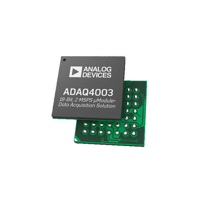
ADAQ4003
Data Sheet
FEATURES
GENERAL DESCRIPTION
Improved design journey
Fully differential ADC driver with selectable input range
Input ranges with 5 V VREF: ±10 V, ±5 V, or ±2.5 V
Essential passive components included
±0.005% iPassives matched resistor array
Wide input common-mode voltage range
High common-mode rejection ratio
Single-ended to differential conversion
Increased signal chain density
Small, 7 mm × 7 mm, 0.80 mm pitch, 49-ball CSP_BGA
4× footprint reduction vs. discrete solution
On-board reference buffer with VCM generation
High performance
Throughput: 2 MSPS, no pipeline delay
Guaranteed 18-bit no missing codes
INL: ±3 ppm typical, ±8 ppm guaranteed
SINAD: 99 dB typical (G = 0.454)
Offset error drift: 0.7 ppm/°C typical (G = 0.454)
Gain error drift: ±0.5 ppm/°C typical
Low total power dissipation: 51.6 mW typical at 2 MSPS
Serial interface SPI-/QSPI™-/MICROWIRE™-/DSP-compatible
Versatile logic interface supply with 1.8 V, 2.5 V, 3 V, or 5 V
The ADAQ4003 is a µModule® precision data acquisition (DAQ),
signal chain solution that reduces the development cycle of a
precision measurement system by transferring the signal chain
design challenge of component selection, optimization, and
layout from the designer to the device.
APPLICATIONS
Automatic test equipment
Machine automation
Process controls
Medical instrumentation
Digital control loops
REF
REF_OUT VDD
Table 1. µModule Data Acquisition Solutions
0.1µF
PD_REF
10kΩ
VCMO
1kΩ
1.1kΩ
IN+
R1K1+
R1K+
1.1kΩ
10kΩ
1nF
33Ω
FDA
ADC
33Ω
1kΩ
1kΩ
Type
16-Bit
18-Bit
2.2µF
0.1µF
1kΩ
VCMO
10µF
1nF
VIO
500 kSPS
ADAQ7988
≥1000 kSPS
ADAQ7980
ADAQ4003
SDI
SCK
SDO
CNV
0.1µF
ADAQ4003
OUT–
VCMO
PD_AMP
VS–
MODE
GND
ADCIN+
ADCIN–
21657-001
OUT+
R1K–
R1K1–
IN–
Using Analog Devices, Inc., iPassives® technology, the
ADAQ4003 also incorporates crucial passive components with
superior matching and drift characteristics to minimize
temperature dependent error sources and to offer optimized
performance (see Figure 1). Housing this signal chain solution
in a small, 7 mm × 7 mm, 0.80 mm pitch, 49-ball CSP_BGA
enables compact form factor designs without sacrificing
performance and simplifies end system bill of materials
management. This level of system integration makes the
ADAQ4003 much less sensitive to printed circuit board (PCB)
layout while still providing flexibility to adapt to a wide range of
signal levels.
The serial peripheral interface (SPI)-compatible, serial user interface
is compatible with 1.8 V, 2.5 V, 3 V, or 5 V logic, using a separate
VIO supply. Specified operation of ADAQ4003 is from −40°C
to +125°C.
FUNCTIONAL BLOCK DIAGRAM
VS+
Using system-in-package (SIP) technology, the ADAQ4003
reduces end system component count by combining multiple
common signal processing and conditioning blocks into a
single device. These blocks include a high resolution 18-bit,
2 MSPS successive approximation register (SAR), analog-todigital converter (ADC), a low noise, fully differential ADC
driver amplifier (FDA), and a stable reference buffer.
Figure 1.
Rev. 0
Document Feedback
Information furnished by Analog Devices is believed to be accurate and reliable. However, no
responsibility is assumed by Analog Devices for its use, nor for any infringements of patents or other
rights of third parties that may result from its use. Specifications subject to change without notice.
No license is granted by implication or otherwise under any patent or patent rights of Analog
Devices. Trademarks and registered trademarks are the property of their respective owners.
One Technology Way, P.O. Box 9106, Norwood, MA 02062-9106, U.S.A.
Tel: 781.329.4700
©2020 Analog Devices, Inc. All rights reserved.
Technical Support
www.analog.com
�ADAQ4003
Data Sheet
TABLE OF CONTENTS
Features .............................................................................................. 1
Analog Inputs ............................................................................. 21
Applications ...................................................................................... 1
Ease of Drive Features ............................................................... 21
Functional Block Diagram .............................................................. 1
Voltage Reference Input............................................................ 23
General Description ......................................................................... 1
Power Supply (Power Tree) ...................................................... 23
Revision History ............................................................................... 2
Digital Interface .......................................................................... 23
Specifications .................................................................................... 3
Register Read and Write Functionality ................................... 24
Timing Specifications .................................................................. 6
Status Word ................................................................................ 26
Absolute Maximum Ratings ........................................................... 8
CS Mode, 3-Wire Turbo Mode ................................................ 27
Thermal Resistance ...................................................................... 8
CS Mode, 3-Wire Without Busy Indicator............................. 28
Electrostatic Discharge (ESD) Ratings ...................................... 8
CS Mode, 3-Wire with Busy Indicator .................................... 29
ESD Caution.................................................................................. 8
CS Mode, 4-Wire Turbo Mode ................................................ 30
Pin Configuration and Function Descriptions ............................ 9
CS Mode, 4-Wire Without Busy Indicator............................. 31
Typical Performance Characteristics ........................................... 11
Terminology .................................................................................... 17
Theory of Operation ...................................................................... 18
Circuit Information ................................................................... 18
Transfer Functions ..................................................................... 18
Applications Information.............................................................. 19
CS Mode, 4-Wire with Busy Indicator .................................... 32
Daisy-Chain Mode ..................................................................... 33
Layout Guidelines ...................................................................... 34
Outline Dimensions ....................................................................... 35
Ordering Guide .......................................................................... 35
Typical Application Diagrams.................................................. 19
REVISION HISTORY
9/2020—Revision 0: Initial Version
Rev. 0 | Page 2 of 35
�Data Sheet
ADAQ4003
SPECIFICATIONS
VDD = 1.8 V ± 5%, VS+ = 5.5 V ± 5%, VS− = 0 V, VIO = 1.7 V to 5.5 V, reference voltage (VREF) = 5 V, sampling frequency (fS) =
2 MSPS, all specifications TMIN to TMAX, high-Z mode disabled, span compression disabled, and turbo mode enabled, unless otherwise
noted. ADC driver configured in single-ended to differential configuration and fast mode, unless otherwise noted.
Table 2.
Parameter
RESOLUTION
ANALOG INPUTS
Input Impedance (ZIN)
Differential Input Voltage Ranges1
Input Capacitance
THROUGHPUT
Complete Cycle
Conversion Time
Acquisition Phase2
Throughput Rate3
Transient Response4
DC ACCURACY
No Missing Codes
Integral Linearity Error (INL)
Test Conditions/Comments
IN+, IN−, R1K1+, R1K1−, R1K+, and R1K−
Single-ended to differential configuration
G = 0.454, input voltage (VIN) = 22 V p-p
G = 0.909, VIN = 11 V p-p
G = 1, VIN = 10 V p-p
G = 1.9, VIN = 5.2 V p-p
Fully differential configuration
G = 0.454 and G = 0.909,
VIN = 22 V p-p and 11 V p-p
G = 1, VIN = 10 V p-p
G = 1.9, VIN = 5.2 V p-p
G = 0.454, VIN = 22 V p-p
G = 0.909, VIN = 11 V p-p
G = 1, VIN = 10 V p-p
G = 1.9, VIN = 5.2 V p-p
IN+ and IN−
Unit
Bit
kΩ
kΩ
kΩ
Ω
1.1
kΩ
1
523
kΩ
Ω
V
V
V
V
pF
−2.2 × VREF
−1.1 × VREF
−VREF
−0.526 × VREF
+2.2 × VREF
+1.1 × VREF
+VREF
+0.526 × VREF
12
290
0
320
2
40
ns
ns
ns
MSPS
μs
Single-ended to differential configuration
All gains, VS− = −1 V
Transition Noise
Gain Error
Gain Error Drift
Offset Error
All gains
All gains
All gains
G = 0.454
G = 0.909, G = 1
G = 1.9
G = 0.454
G = 0.909 and G = 1
G = 1.9
Fully differential configuration, all gains
Negative
1/f Noise6
Input Current Noise
Max
1.3
1.44
1.33
778
290
All gains, VS− = −1 V
Common-Mode Rejection Ratio (CMRR)
Power Supply Rejection Ratio (PSRR)
Positive
Typ
500
Differential Linearity Error (DNL)
Offset Error Drift
Min
18
VDD = 1.71 V to 1.89 V
VS+ = 5.225 V to 5.775 V, VS− = 0 V
VS+ = +5.5 V, VS− = 0 V to −0.5 V
Bandwidth = 0.1 Hz to 10 Hz
Input frequency (fIN) = 100 kHz
Rev. 0 | Page 3 of 35
18
−8
−2.1
−1
−3.8
−0.05
−3
−1
−0.9
−1.5
−8
−10
−15
±3
±0.8
±0.4
±2.66
0.93
±0.005
±0.5
±0.1
±0.06
±0.01
+0.7
+1.6
+2.6
90
72
110
107
38
1
+8
+2.1
+1
+3.8
+0.05
+3
+1
+0.9
+1.5
+8
+10
+15
Bits
ppm
LSB5
LSB5
ppm
LSB
%FS
ppm/°C
mV
mV
mV
ppm/°C
ppm/°C
ppm/°C
dB
dB
dB
dB
μV p-p
pA/√Hz
�ADAQ4003
Parameter
AC ACCURACY
Dynamic Range
Oversampled Dynamic Range
Total RMS Noise
Signal-to-Noise Ratio (SNR)
Signal-to-Noise + Distortion (SINAD)
Total Harmonic Distortion (THD)
Spurious-Free Dynamic Range (SFDR)
−3 dB Input Bandwidth
Recovery Time
Input Overdrive
Output Overdrive
Clamp
Aperture Delay
Aperture Jitter
REFERENCE
VREF Range
Input Current (IREF)
REF_OUT Current (IREF_OUT)
Data Sheet
Test Conditions/Comments
Single-ended to differential and fully
differential configuration
All gains, −60 dBFS
G = 0.454
G = 0.909 and G = 1
G = 1.9
Oversampling ratio (OSR) = 2, all gains
OSR = 256, all gains
All gains
fIN = 1 kHz, −0.5 dBFS
G = 0.454
G = 0.909 and G =1
G = 1.9
fIN = 100 kHz, G = 0.909
fIN = 400 kHz, G = 0.909
Low power mode enabled, G = 0.909
VS+ = 3.3 V, VS− = 0 V,
VREF = 2.5 V, G = 0.909
fIN = 1 kHz, −0.5 dBFS
G = 0.454
G = 0.909 and G =1
G = 1.9
fIN = 100 kHz, G = 0.909
fIN = 400 kHz, G = 0.909
Low power mode enabled, G = 0.909
VS+ = 3.3 V, VS− = 0 V,
VREF = 2.5 V, G = 0.909
fIN = 1 kHz, −0.5 dBFS, all gains
fIN = 100 kHz, G = 0.909
fIN = 400 kHz, G = 0.909
Low power mode enabled, G = 0.909
VS+ = 3.3 V, VS− = 0 V,
VREF = 2.5 V, G = 0.909
fIN = 1 kHz, −0.5 dBFS, all gains
fIN = 100 kHz, G = 0.909
fIN = 400 kHz, G = 0.909
Low power mode enabled, G = 0.909
VS+ = 3.3 V, VS− = 0 V,
VREF = 2.5 V, G = 0.909
Min
Rev. 0 | Page 4 of 35
Max
94.5
Unit
99.5
97
98
98
92
96
92
dB
dB
dB
dB
dB
dB
µV rms
dB
dB
dB
dB
dB
dB
dB
dB
99
96.5
97.5
97.5
91.5
95.5
91.5
dB
dB
dB
dB
dB
dB
dB
dB
−120
−100
−95
−110
−118
dB
dB
dB
dB
dB
122
101
95
110
118
dB
dB
dB
dB
dB
4.4
MHz
280
120
100
1
1
ns
ns
ns
ns
ps rms
100
97.5
98.5
103
122
35.35
94.2
94
All gains
All gains
All gains
Buffer enabled
Buffer enabled
Buffer disabled, 2 MSPS, VREF = 5 V
Typ
2.4
5.1 or VS+ − 0.08
60
1.27
V
µA
mA
�Data Sheet
Parameter
VCMO
VCMO Voltage (VVCMO) 7
Output Impedance
DIGITAL INPUTS
Logic Levels
Input Low Voltage (VIL)
Input High Voltage (VIH)
Input Low Current (IIL)
Input High Current (IIH)
Input Pin Capacitance
DIGITAL OUTPUTS 8
Data Format
Output Low Voltage (VOL)
Output High Voltage (VOH)
POWER-DOWN AND MODE SIGNALING
ADC Driver and Reference Buffer
PD_AMP, PD_REF, and MODE Voltage
Low
High
POWER REQUIREMENTS
VDD
VS+
VS−
VIO
Total Standby Current 9, 10
Power-Down Current
Power Dissipation
VS+
VDD
VIO
Total
ADAQ4003
Test Conditions/Comments
Min
Typ
Max
Unit
VREF/2 − 0.003
VREF/2
5
VREF/2 + 0.003
V
kΩ
+0.3 × VIO
+0.2 × VIO
VIO + 0.3
VIO + 0.3
+1
+1
V
V
V
V
µA
µA
pF
SDI, SCK, and CNV
VIO > 2.7 V
VIO ≤ 2.7 V
VIO > 2.7 V
VIO ≤ 2.7 V
−0.3
−0.3
0.7 × VIO
0.8 × VIO
−1
−1
6
Sink current (ISINK) = +500 µA
Source current (ISOURCE) = −500 µA
Twos complement
0.4
VIO − 0.3
Powered down, low power mode
Enabled, fast mode
1.7
1.71
3
VS+ − 10
1.7
Static, all devices enabled
ADC driver, reference buffer disabled
VDD = VIO = 1.8 V, VS+ = 5.5 V, VS− = 0 V
1.8
5.5
0
V
V
V
V
11
100
1.89
VS− + 10
0.1
5.5
14
250
V
V
V
V
mA
nA
41.5
9.5
0.6
51.6
51.5
12
0.7
64.2
mW
mW
mW
mW
44
12.8
0.6
57.4
53
16.5
0.7
70.2
mW
mW
mW
mW
+125
°C
VDD = VIO = 1.8 V, VS+ = 5 V, VS− = 0 V,
high-Z mode enabled
VS+
VDD
VIO
Total
TEMPERATURE RANGE
Specified Performance
TMIN to TMAX
−40
VIN must be within the allowed input common-mode range as per Figure 35, Figure 36, and Figure 37 and is dependent on the VS+ and VS− supply rails used.
The acquisition phase is the time available for the input sampling capacitors to acquire a new input with the ADC running at a throughput rate of 2 MSPS.
3
A throughput rate of 2 MSPS can only be achieved with turbo mode enabled and a minimum SCK rate of 75 MHz. Refer to Table 5 for the maximum achievable
throughput for different modes of operation.
4
Transient response is the time required for the ADAQ4003 to acquire a full-scale input step to ±1 LSB accuracy.
5
The weight of the LSB, referred to input, changes depending on the input voltage range. See Table 10 for the LSB size.
6
See the 1/f noise plot in Figure 28.
7
The VCMO voltage can be used for other circuitry, but it should be driven with a buffer to ensure the VCMO voltage remains stable as per the specified range.
8
There is no pipeline delay. Conversion results are available immediately after a conversion is completed.
9
With all digital inputs forced to VIO or GND as required.
10
The total standby current during the acquisition phase.
1
2
Rev. 0 | Page 5 of 35
�ADAQ4003
Data Sheet
TIMING SPECIFICATIONS
VDD = 1.8 V ± 5%, VS+ = 5.5 V ± 5%, VS− = 0 V, VIO = 1.71 V to 5.5V, VREF = 5 V, fS = 2 MSPS, all specifications TMIN to TMAX, high-Z
mode disabled, span compression disabled, and turbo mode enabled, unless otherwise noted.
Table 3. Digital Interface Timing
Parameter
Conversion Time—CNV Rising Edge to Data Available
Acquisition Phase 1
Time Between Conversions
CNV Pulse Width (CS Mode) 2
Symbol
tCONV
tACQ
tCYC
tCNVH
SCK Period (CS Mode) 3
tSCK
VIO > 2.7 V
VIO > 1.7 V
SCK Period (Daisy-Chain Mode) 4
VIO > 2.7 V
VIO > 1.7 V
SCK Low Time
SCK High Time
SCK Falling Edge to Data Remains Valid Delay
SCK Falling Edge to Data Valid Delay
VIO > 2.7 V
VIO > 1.7 V
CNV or SDI Low to SDO D17 MSB Valid Delay (CS Mode)
Min
Typ
290
Max
320
290
500
10
Unit
ns
ns
ns
ns
9.8
12.3
ns
ns
20
25
3
3
1.5
ns
ns
ns
ns
ns
tSCK
tSCKL
tSCKH
tHSDO
tDSDO
7.5
10.5
ns
ns
10
13
ns
ns
ns
ns
ns
tEN
VIO > 2.7 V
VIO > 1.7 V
CNV Rising Edge to First SCK Rising Edge Delay
Last SCK Falling Edge to CNV Rising Edge Delay
CNV or SDI High or Last SCK Falling Edge to SDO High Impedance (CS Mode)
tQUIET1
tQUIET2
tDIS
190
60
SDI Valid Setup Time from CNV Rising Edge
SDI Valid Hold Time from CNV Rising Edge (CS Mode)
tSSDICNV
tHSDICNV
2
2
ns
ns
SCK Valid Hold Time from CNV Rising Edge (Daisy-Chain Mode)
SDI Valid Setup Time from SCK Rising Edge (Daisy-Chain Mode)
SDI Valid Hold Time from SCK Rising Edge (Daisy-Chain Mode)
tHSCKCNV
tSSDISCK
tHSDISCK
12
2
2
ns
ns
ns
20
The acquisition phase is the time available for the input sampling capacitors to acquire a new input with the ADC running at a throughput rate of 2 MSPS.
For turbo mode, tCNVH must match the tQUIET1 minimum.
3
A throughput rate of 2 MSPS can only be achieved with turbo mode enabled and a minimum SCK rate of 75 MHz.
4
A 50% duty cycle is assumed for SCK.
1
2
Rev. 0 | Page 6 of 35
�Data Sheet
ADAQ4003
Table 4. Register Read and Write Timing
Parameter
READ AND WRITE OPERATION
CNV Pulse Width 1
SCK Period
VIO > 2.7 V
VIO > 1.7 V
SCK Low Time
SCK High Time
READ OPERATION
CNV Low to SDO D17 MSB Valid Delay
VIO > 2.7 V
VIO > 1.7 V
SCK Falling Edge to Data Remains Valid
SCK Falling Edge to Data Valid Delay
VIO > 2.7 V
VIO > 1.7 V
CNV Rising Edge to SDO High Impedance
WRITE OPERATION
SDI Valid Setup Time from SCK Rising Edge
SDI Valid Hold Time from SCK Rising Edge
CNV Rising Edge to SCK Edge Hold Time
CNV Falling Edge to SCK Active Edge Setup Time
1
Symbol
Min
tCNVH
tSCK
10
ns
9.8
12.3
3
3
ns
ns
ns
ns
tSCKL
tSCKH
Typ
Max
Unit
tEN
tHSDO
tDSDO
ns
ns
ns
7.5
10.5
20
ns
ns
ns
1.5
tDIS
tSSDISCK
tHSDISCK
tHCNVSCK
tSCNVSCK
10
13
2
2
0
6
ns
ns
ns
ns
For turbo mode, tCNVH must match the tQUIET1 minimum.
Y% VIO1
X% VIO1
tDELAY
tDELAY
VIH2
VIL2
1FOR
VIO ≤ 2.7V, X = 80, AND Y = 20; FOR VIO > 2.7V, X = 70, AND Y = 30.
VIH AND MAXIMUM VIL USED. SEE DIGITAL INPUTS
SPECIFICATIONS IN TABLE 2.
2MINIMUM
21657-002
VIH2
VIL2
Figure 2. Voltage Levels for Timing
Table 5. Achievable Throughput for Different Modes of Operation
Parameter
THROUGHPUT, CS MODE
3-Wire and 4-Wire Turbo Mode
3-Wire and 4-Wire Turbo Mode and Six Status Bits
3-Wire and 4-Wire Mode
3-Wire and 4-Wire Mode and Six Status Bits
Test Conditions/Comments
fSCK = 100 MHz, VIO ≥ 2.7 V
fSCK = 80 MHz, VIO < 2.7 V
fSCK = 100 MHz, VIO ≥ 2.7 V
fSCK = 80 MHz, VIO < 2.7 V
fSCK = 100 MHz, VIO ≥ 2.7 V
fSCK = 80 MHz, VIO < 2.7 V
fSCK = 100 MHz, VIO ≥ 2.7 V
fSCK = 80 MHz, VIO < 2.7 V
Rev. 0 | Page 7 of 35
Min
Typ
Max
Unit
2
2
2
1.78
1.75
1.62
1.59
1.44
MSPS
MSPS
MSPS
MSPS
MSPS
MSPS
MSPS
MSPS
�ADAQ4003
Data Sheet
ABSOLUTE MAXIMUM RATINGS
THERMAL RESISTANCE
Table 6.
Parameter
Analog Inputs
R1K+, R1K−, R1K1+, R1K1− to GND1
Supply Voltage
REF_OUT and VIO to GND
VDD to GND
VDD to VIO
VS+ to VS−
VS+ to GND
VS− to GND
Digital Inputs to GND
Digital Outputs to GND
Temperature
Storage Range
Junction
Lead Soldering
1
2
Thermal performance is directly linked to PCB design and
operating environment. Careful attention to PCB thermal
design is required.
Rating
−16 V to +16 V2 or
±18 mA2
θJA is the natural convection, junction to ambient thermal
resistance measured in a one cubic foot sealed enclosure, and
θJC is the junction to case thermal resistance.
−0.3 V to +6.0 V
−0.3 V to +2.1 V
−6 V to +2.4 V
11 V
−0.3 V to +11 V
−11 V to +0.3 V
−0.3 V to VIO + 0.3 V
−0.3 V to VIO + 0.3 V
Table 7. Thermal Resistance
Package Type1
BC-49-5
1
θJA
53.5
θJC
54.9
Unit
°C/W
JEDEC Board Layers
2S2P
Test Condition 1: thermal impedance simulated values are based upon use
of a 2S2P JEDEC standard PCB configuration per JEDEC Standard JESD51-7.
ELECTROSTATIC DISCHARGE (ESD) RATINGS
−65°C to +150°C
150°C
260°C reflow as per
JEDEC J-STD-020
The following ESD information is provided for handling of
ESD-sensitive devices in an ESD protected area only.
Human body model (HBM) per ANSI/ESDA/JEDDEC JS-001.
See the Analog Inputs section.
The iPassives resistors can sustain specified maximum voltage and current
indefinitely.
Stresses at or above those listed under Absolute Maximum
Ratings may cause permanent damage to the product. This is a
stress rating only; functional operation of the product at these
or any other conditions above those indicated in the operational
section of this specification is not implied. Operation beyond
the maximum operating conditions for extended periods may
affect product reliability.
Field induced charged device model (FICDM) per ANSI/
ESDA/JEDEC JS-002.
ESD Ratings for the ADAQ4003
Table 8. ADAQ4003, 49-Ball CSP_BGA
ESD Model
HBM
FICDM
ESD CAUTION
Rev. 0 | Page 8 of 35
Withstand Threshold (V)
4000
1000
Class
2
C4
�Data Sheet
ADAQ4003
PIN CONFIGURATION AND FUNCTION DESCRIPTIONS
A1 BALL
CORNER
1
2
3
4
5
6
1
2
3
4
5
6
7
A
GND
VDD
OUT+
VS–
REF_OUT
REF
GND
B
R1K−
R1K−
OUT+
VS–
GND
VIO
VIO
C
R1K1−
R1K1−
VS–
VS–
DNC
PD_AMP
SDI
D
IN−
IN+
DNC
DNC
DNC
PD_REF
SCK
E
R1K1+
R1K1+
MODE
VS+
ADCIN+
GND
SDO
F
R1K+
R1K+
OUT–
VS+
DNC
DNC
CNV
G
GND
VCMO
OUT−
VS+
VS+
ADCIN−
GND
7
A
B
C
D
21657-003
F
G
21657-004
E
Figure 4. Ball Configuration
Figure 3. Ball Configuration, Top View
Table 9. Ball Function Descriptions
Ball No.
A1, A7, B5, E6, G1, G7
A2
A3, B3
A4, B4, C3, C4
A5
A6
B1, B2
B6, B7
Mnemonic
GND
VDD
OUT+
VS−
REF_OUT
REF
R1K−
VIO
Type 1
P
P
AO
P
AO
AI
AI
P
C1, C2
C5, D3 to D5, F5, F6
C6
R1K1−
DNC
PD_AMP
AI
N/A
DI
C7
SDI
DI
Description
Power Supply Ground.
1.8 V Power Supply. The VDD range is 1.71 V to 1.89 V.
Positive Output of the Fully Differential ADC Driver.
Negative Supply of the Fully Differential ADC Driver.
Reference Buffer Output Voltage.
Reference Buffer Input Voltage.
1 kΩ Resistor Input to Negative Input of the Fully Differential ADC Driver.
Input and Output Interface Digital Power. Nominally, the VIO pins are at the same supply as
the host interface (1.8 V, 2.5 V, 3 V, or 5 V).
1.1 kΩ Resistor Input to Negative Input of the Fully Differential ADC Driver.
Do Not Connect. Do not connect to this pin.
Power-Down Amplifier. Active low. Connect the PD_AMP pin to GND to power down the
fully differential ADC driver. Otherwise, connect the PD_AMP pin to logic high.
Serial Data Input. This input provides multiple features. SDI selects the interface mode of
the ADC as follows:
Daisy-chain mode is selected if SDI is low during the CNV rising edge. In this mode, SDI is
used as a data input to daisy-chain the conversion results of two or more ADCs onto a
single SDO line. The digital data level on SDI is output on SDO with a delay of 18 SCK cycles.
CS mode is selected if SDI is high during the CNV rising edge. In this mode, either SDI or
CNV can enable the serial output signals when low. If SDI or CNV is low when the conversion
is complete, the busy indicator feature is enabled. With CNV low, the device can be
programmed by clocking in a 16-bit word on SDI on the rising edge of SCK.
Rev. 0 | Page 9 of 35
�ADAQ4003
Data Sheet
Ball No.
D1
D2
D6
Mnemonic
IN−
IN+
PD_REF
Type 1
AI
AI
DI
Description
Negative Input of the Fully Differential ADC Driver.
Positive Input of the Fully Differential ADC Driver.
Power-Down Reference Buffer. Active low. Connect the PD_REF pin to GND to power down
the reference buffer. Otherwise, connect the PD_REF pin to logic high.
D7
SCK
DI
E1, E2
E3
R1K1+
MODE
AI
DI
E4, F4, G4, G5
E5
VS+
ADCIN+
P
AO
E7
F1, F2
F3, G3
F7
SDO
R1K+
OUT−
CNV
DO
AI
AO
DI
G2
G6
VCMO
ADCIN−
AO
AO
Serial Data Clock Input. When the device is selected, the conversion result is shifted out by
this clock.
1.1 kΩ Resistor Input to Positive Input of the Fully Differential ADC Driver.
Power Mode for the Fully Differential ADC Driver. Full performance when the MODE pin is
high, and low power mode when the MODE pin is low.
Fully Differential ADC Driver and Reference Buffer Positive Supply.
Positive Input to the ADC. Extra capacitance can be added on the ADCIN+ pin to reduce the
RC filter bandwidth.
Serial Data Output. The conversion result is output on the SDO pin. SDO synchronizes to SCK.
1 kΩ Resistor Input to Positive Input of the Fully Differential ADC Driver.
Negative Output of the Fully Differential ADC Driver.
Convert Input. This input has multiple functions. On its leading edge, CNV initiates the
conversions and selects the interface mode of the device: daisy-chain mode or CS mode.
In CS mode, the SDO pin is enabled when CNV is low. In daisy-chain mode, the data is read
when CNV is high.
Fully Differential ADC Driver Output Common-Mode Voltage. Nominally, VREF/2.
Negative Input to the ADC. Extra capacitance can be added on the ADCIN− pin to reduce
the RC filter bandwidth.
1
P is power, AO is analog output, AI is analog input, N/A is not applicable, DI is digital input, and DO is digital output.
Rev. 0 | Page 10 of 35
�Data Sheet
ADAQ4003
TYPICAL PERFORMANCE CHARACTERISTICS
VS+ = 5.5 V, VS− = 0 V, VDD = 1.8 V, VIO = 3.3 V, VREF = 5 V, TA = 25°C, high-Z mode disabled, span compression disabled, turbo
mode enabled, and fS = 2 MSPS, unless otherwise noted.
1.0
0.5
–40°C
+25°C
125°C
0.6
0.3
0.4
0.2
0.2
0.1
0
–0.1
–0.4
–0.2
–0.6
–0.3
–0.8
–0.4
32768
65536
–0.5
21657-105
–1.0
98304 131072 163840 196608 229376 262144
CODE
0
65536
98304 131072 163840 196608 229376 262144
CODE
Figure 8. DNL vs. Code for Various Temperatures, VREF = 5 V, G = 0.454
Figure 5. INL vs. Code for Various Temperatures, VREF = 5 V, G = 0.454
400000
0
160
32768
21657-108
0
–0.2
0
–40°C
+25°C
+125°C
0.4
DNL (LSB)
INL (LSB)
0.8
140
VREF = 5V
VREF = 2.5V
350000
–50
120
80
–150
60
40
–200
20
250000
COUNTS
–100
PHASE (Degrees)
200000
150000
100000
0
–250
50000
–20
1
10
100
1k
10k
100k
1M
10M
100M
–300
1G
0
21657-007
–40
FREQUENCY (Hz)
Figure 6. ADC Driver Open-Loop Gain and Phase vs. Frequency
–23
–19
–17
–15
–13
–11
–9
–7
–5
–3
CODES
Figure 9. Histogram of a DC Input at the Code Center, VREF = 2.5 V and VREF = 5 V
2.9
400000
VREF = 5V
VREF = 2.5V
2.7
350000
2.5
2.3
300000
G
G
G
G
G
G
G
G
2.1
1.9
1.7
1.5
= 0.454, VREF = 5V
= 0.454, VREF = 2.5V
= 0.909, VREF = 5V
= 0.909, VREF = 2.5V
= 1, VREF = 5V
= 1, VREF = 2.5V
= 1.9, VREF = 5V
= 1.9, VREF = 2.5V
250000
COUNTS
TRANSITION NOISE (LSB)
–21
21657-005
OPEN-LOOP GAIN (dB)
300000
100
200000
150000
1.3
1.1
100000
0.9
–20
0
20
40
60
TEMPERATURE (°C)
80
100
120
0
21657-110
0.5
–40
–23
–21
–19
–17
–15
–13
CODES
Figure 7. Transition Noise vs. Temperature for G = 0.454, G = 0.909, G = 1, and
G = 1.9 and VREF = 5 V and VREF = 2.5 V
–11
–9
–7
–5
–3
21657-006
50000
0.7
Figure 10. Histogram of a DC Input at the Code Transition, VREF = 2.5 V and
VREF = 5 V
Rev. 0 | Page 11 of 35
�ADAQ4003
Data Sheet
–20
–40
–40
–60
–60
–80
–100
–120
–120
–160
–160
10k
FREQUENCY (Hz)
100k
1M
–180
100
21657-112
1k
100k
1M
Figure 14. 1 kHz, −0.5 dBFS Input Tone FFT, Wide View, G = 1,
VREF = 2.5 V, Single-Ended
VREF = 5V
SNR = 97.5dB
THD = –117.9dB
SINAD= 97.4dB
–20
–40
–60
–80
–100
–60
–80
–100
–120
–120
–140
–140
–160
–160
10k
FREQUENCY (Hz)
100k
1M
–180
100
21657-113
1k
0
VREF = 2.5V
SNR = 93.3dB
THD = –117.8dB
SINAD = 93.1dB
–20
10k
FREQUENCY (Hz)
100k
1M
Figure 15. 1 kHz, −0.5 dBFS Input Tone FFT, Wide View, Differential,
G = 0.909, VREF = 5 V, Low Power Mode
Figure 12. 1 kHz, −0.5 dBFS Input Tone FFT, Wide View, G = 1,
VREF = 5 V, Single-Ended
0
1k
21657-117
AMPLITUDE (dB)
–40
–20
VREF = 5V
SNR = 95.3dB
THD = –105.3dB
SINAD = 94.9dB
–40
–60
–80
–100
–60
–80
–100
–120
–120
–140
–140
–160
–160
10k
FREQUENCY (Hz)
100k
1M
–180
100
21657-115
1k
Figure 13. 1 kHz, −0.5 dBFS Input Tone FFT, Wide View, G = 1, VREF = 2.5 V,
Differential
1k
10k
FREQUENCY (Hz)
100k
1M
21657-118
AMPLITUDE (dB)
–40
–180
100
10k
FREQUENCY (Hz)
VREF = 5V
SNR = 98.1dB
THD = –117.9dB
SINAD = 98.0dB
–20
–180
100
1k
0
0
AMPLITUDE (dB)
–100
–140
Figure 11. 1 kHz, −0.5 dBFS Input Tone Fast Fourier Transform (FFT),
Wide View, G = 1,VREF = 5 V, Differential
AMPLITUDE (dB)
–80
–140
–180
100
VREF = 2.5V
SNR = 93.1dB
THD = –112.1dB
SINAD = 92.9dB
–20
AMPLITUDE (dB)
AMPLITUDE (dB)
0
VREF = 5V
SNR = 98.2dB
THD = –123.1dB
SINAD = 98.1dB
21657-116
0
Figure 16. 100 kHz, −0.5 dBFS Input Tone FFT, Wide View, G = 1, VREF = 5 V
Rev. 0 | Page 12 of 35
�Data Sheet
ADAQ4003
0
VREF = 2.5V
SNR = 92.4dB
THD = –113.7dB
SINAD = 92.2dB
–20
–40
–40
–60
–60
AMPLITUDE (dB)
–80
–100
–120
–100
–120
–140
–160
–160
10k
100k
1M
–180
100
21657-120
1k
FREQUENCY (Hz)
98
100k
1M
16.5
100
98
15.95
16.0
96
15.55
95
94
93
3.0
3.5
4.0
4.5
15.35
90
14.5
G
G
G
G
G
G
15.15
86
14.95
5.0
REFERENCE VOLTAGE (V)
Figure 18. SNR, SINAD, and Effective Number of Bits (ENOB) vs. Reference
Voltage for G = 0.454, G = 0.909, and G = 1.9, fIN = 1 kHz
99.0
15.0
92
88
84
21657-039
G = 0.454 SNR
G = 0.454 SINAD
G = 0.454 ENOB
G = 0.909 SNR
G = 0.909 SINAD
G = 0.909 ENOB
G = 1.9 SNR
G = 1.9 SINAD
G = 1.9 ENOB
15.5
94
ENOB (Bits)
96
ENOB (Bits)
15.75
SNR, SINAD (dB)
97
92
2.5
10k
Figure 20. 400 kHz, −0.5 dBFS Input Tone FFT, G = 1, Wide View, VREF = 5 V
16.15
99
1k
FREQUENCY (Hz)
Figure 17. 1 kHz, −0.5 dBFS Input Tone FFT, Wide View, Differential,
G = 0.909, VREF = 2.5 V, Low Power Mode
SNR, SINAD (dB)
–80
–140
–180
100
VREF = 5V
SNR = 88.3dB
THD = –87.6dB
SINAD = 85.7dB
= 1.9 SNR
= 1.9 SINAD
= 1.9 ENOB
= 0.909 SNR
= 0.909 SINAD
= 0.909 ENOB
1k
14.0
10k
13.5
1M
100k
21657-123
AMPLITUDE (dB)
–20
21657-150
0
FREQUENCY (Hz)
Figure 21. SNR, SINAD, and ENOB vs. Frequency for G = 1.9 and G = 0.909,
VREF = 5 V
16.15
–112
16.10
–114
16.05
–116
G = 0.454
G = 0.909
G = 1.9
98.8
16.00
98.0
15.95
97.8
97.6
THD (dB)
98.2
–118
–120
15.90
–122
15.85
–124
15.80
–126
G = 1.9 SNR
G = 1.9 SINAD
G = 1.9 ENOB
97.0
–40
–20
0
97.2
G = 0.909 SNR
G = 0.454 SNR
G = 0.909 SINAD G = 0.454 SINAD
G = 0.909 ENOB
G = 0.454 ENOB
20
40
60
80
100
120
TEMPERATURE (°C)
Figure 19. SNR, SINAD, and ENOB vs. Temperature,
G =1.9, G = 0.909, and G = 0.454, fIN = 1 kHz
2.5
3.0
3.5
4.0
REFERENCE VOLTAGE (V)
4.5
5.0
21657-043
97.4
21657-040
SNR, SINAD (dB)
98.4
ENOB (Bits)
98.6
Figure 22. THD vs. Reference Voltage, G = 0.454, G = 0.909, and G = 1.9,
fIN = 1 kHz
Rev. 0 | Page 13 of 35
�ADAQ4003
Data Sheet
–112
126
G = 0.454
G = 0.909
G = 1.9
–114
G = 0.454
G = 0.909
G = 1.9
124
–116
SFDR (dB)
THD (dB)
122
–118
–120
120
118
–122
0
20
40
60
80
100
120
TEMPERATURE (°C)
114
–40
0.25
–90
125
0.20
–95
120
–100
115
–115
100
–120
95
–125
90
–130
10k
1k
60
80
100
120
= 0.454
= 0.909
=1
= 1.9
0.10
0.05
0
–0.05
–0.10
–0.15
FREQUENCY (Hz)
Figure 24. THD and SFDR vs. Frequency for G = 0.909 and G = 1.9, VREF = 5 V
–0.25
–40
–20
0
20
40
60
TEMPERATURE (°C)
80
100
120
Figure 27. Offset Error vs. Temperature for G = 0.454, G = 0.909, G = 1, and
G = 1.9
126
39.5
ADC OUTPUT VOLTAGE (µV)
124
122
SFDR (dB)
40
–0.20
85
1M
100k
OFFSET ERROR (mV)
105
SFDR (dB)
–110
110
G
G
G
G
0.15
21657-126
THD (dB)
130
= 0.909 SFDR
= 1.9 SFDR
= 1.9 THD
= 0.909 THD
20
Figure 26. SFDR vs. Temperature for G = 0.454, G = 0.909, and G = 1.9,
fIN = 1kHz
–85
G
G
G
G
0
TEMPERATURE (°C)
Figure 23. THD vs. Temperature for G = 0.454, G = 0.909, and G = 1.9,
fIN = 1 kHz
–105
–20
21657-130
–20
21657-041
–126
–40
21657-045
116
–124
120
118
116
39.0
38.5
38.0
37.5
2.5
3.0
3.5
4.0
REFERENCE VOLTAGE (V)
4.5
5.0
Figure 25. SFDR vs. Reference Voltage for G = 0.454, G = 0.909, and G = 1.9,
fIN = 1 kHz
Rev. 0 | Page 14 of 35
37.0
0
1
2
3
4
5
6
7
8
9
10
TIME (Seconds)
Figure 28. 1/f Noise for 0.1 Hz to 10 Hz Bandwidth, 100 kSPS,
250 Samples Averaged per Reading
21657-048
114
21657-044
G = 0.454
G = 0.909
G = 1.9
�ADAQ4003
10
20
9
18
8
16
7
14
POWER (mW)
6
5
4
VDD, HIGH-Z DISABLED
VDD, HIGH-Z ENABLED
VIO, HIGH-Z DISABLED
VIO, HIGH-Z ENABLED
VS+, HIGH-Z DISABLED
VS+, HIGH-Z ENABLED
3
2
VDD
VIO
REF
TOTAL POWER
12
10
8
6
4
1
2
–5
25
85
125
TEMPERATURE (°C)
0
100
21657-131
0
–40
1k
10k
100k
21657-137
OPEARTING CURRENT (mA)
Data Sheet
1M
THROUGHPUT (Hz)
Figure 29. Operating Current vs. Temperature, 2 MSPS
Figure 32. Power vs. Throughput
30
130
25
POSITIVE FULL-SCALE ERROR, G = 0.454
POSITIVE FULL-SCALE ERROR, G = 0.909
POSITIVE FULL-SCALE ERROR, G = 1.9
NEGATIVE FULL-SCALE ERROR, G = 0.454
NEGATIVE FULL-SCALE ERROR, G = 0.909
NEGATIVE FULL-SCALE ERROR, G = 1.9
20
10
110
PSRR (dB)
GAIN ERROR (LSB)
15
120
5
0
–5
100
90
VS+
VS–
VDD
80
–10
–15
70
–20
25
85
125
TEMPERATURE (°C)
50
100
125
120
115
120
= 0.454, DYNAMIC RANGE
= 0.454, fIN = 1kHz
= 0.454, fIN = 10kHz
= 0.909, DYNAMIC RANGE
= 0.909, fIN = 1kHz
= 0.909, fIN = 10kHz
= 1.9, DYNAMIC RANGE
= 1.9, fIN = 1kHz
= 1.9, fIN = 10kHz
100
110
105
90
80
70
100
60
95
50
90
0
2
4
8
16
32
1M
G = 0.454
G = 0.909
G = 1.9
110
64
128
OVERSAMPLING RATE (OSR)
256
512
1024
21657-133
DYNAMIC RANGE AND SNR (dB)
130
100k
Figure 33. PSRR vs. Frequency
CMRR (dB)
G
G
G
G
G
G
G
G
G
10k
FREQUENCY (Hz)
Figure 30. Gain Error vs. Temperature for Positive Full-Scale Error and
Negative Full-Scale Error and for G = 0.454, G = 0.909, and G = 1.9
135
1k
Figure 31. Dynamic Range and SNR vs. Oversampling Rate for G = 0.454,
G = 0.909, and G = 1.9, and for Input Frequencies, 2 MSPS
Rev. 0 | Page 15 of 35
40
100
1k
10k
FREQUENCY (Hz)
100k
1M
21657-136
–5
21657-233
–30
–40
21657-135
60
–25
Figure 34. CMRR vs. Frequency for G = 0.454, G = 0.909, and G = 1.9
�ADAQ4003
–4.55, +10
8
+4.55, +10
+4.55, +8
–4.55, +8
INPUT COMMON-MODE VOLTAGE (V)
6
VS = ±5V
VS = +5.5V/0V
VS = +5.5V/–1V
3
–0
–3
–4.55, –5.5
+4.55, –5.5
0, –6
–6
+4.55, –8.8
–4.55, –8.8
0, –9.3
–9
–4.55, –10.5
–12
–5
–4
–3
–2
–1
0
–4.77, +5
4
2
0
2
3
4
5
–4.77, –1.43
+4.77, –1.43
0, –1.43
–2
0, –2.91
–4
–4.77, –2.95
+4.77, –2.95
–6
–10
+4.77, –8.85
–4.77, –8.85
0, –8.9
–4.55, +7.15
–4.55, +7.15
–5
–4
–3
–2
–1
0
1
2
3
4
5
FDA OUTPUT VOLTAGE (V)
Figure 35. Input Common-Mode Voltage vs. FDA Output Voltage, G = 0.454,
Differential Input
9
+4.77, +5
VS = ±5V
VS = +5.5V/0V
VS = +5.5V/–1V
+4.55, –10.5
1
FDA OUTPUT VOLTAGE (V)
Figure 37. Input Common-Mode Voltage vs. FDA Output Voltage, G = 1.9,
Differential Input
5
+4.55, +7.15
+4.55, +7.15
6
0
–4.55, +6
+4.55, +6
3
–5
–4.55, –2.4
+4.55, –2.4
0, –2.8
–3
GAIN (dB)
0
0, –4.8
–4.55, –4.8
–15
+4.55, –4.8
VS = ±5V
VS = +5.5V/0V
VS = +5.5V/–1V
–9
–20
–25
–12
–15
–10
–4.55, –13.25
–5
–4
–3
+4.55, –13.25
0, –13.25
–2
–1
0
1
2
FDA OUTPUT VOLTAGE (V)
3
4
5
–30
0.1
G
G
G
G
G
G
= 1.9, FULL POWER
= 1.9, LOW POWER
= 0.454, FULL POWER
= 0.454, LOW POWER
= 0.909, FULL POWER
= 0.909, LOW POWER
1
10
FREQUENCY (MHz)
100
21657-134
–6
21657-046
INPUT COMMON-MODE VOLTAGE (V)
6
–8
0, –10.5
+4.77, +5.93
+4.77, +5.93
–4.77, +5.93
–4.77, +5.93
21657-047
9
10
+4.55, +10
–4.55, +10
21657-042
INPUT COMMON-MODE VOLTAGE (V)
12
Data Sheet
Figure 38. Small Signal Frequency Response and 0.1 dB Flatness for
G = 1.9, G = 0.454, and G = 0.909 at Full Power and Low Power
Figure 36. Input Common-Mode Voltage vs. FDA Output Voltage,
G = 0.909, Differential Input
Rev. 0 | Page 16 of 35
�Data Sheet
ADAQ4003
TERMINOLOGY
Integral Nonlinearity (INL) Error
INL error is the deviation of each individual code from a line
drawn from negative full scale through positive full scale. The
point used as negative full scale occurs ½ LSB before the first
code transition. Positive full scale is defined as a level 1½ LSB
beyond the last code transition. The deviation is measured from
the middle of each code to the true straight line (see Figure 39).
Differential Nonlinearity (DNL) Error
In an ideal ADC, code transitions are 1 LSB apart. DNL is the
maximum deviation from this ideal value. DNL error is often
specified in terms of resolution for which no missing codes are
guaranteed.
Offset Error
Offset error is the difference between the ideal midscale voltage,
0 V, and the actual voltage producing the midscale output code,
0 LSB.
Gain Error
The first transition (from 100 … 00 to 100 … 01) occurs at
a level ½ LSB above nominal negative full scale. The last
transition (from 011 … 10 to 011 … 11) occurs for an analog
voltage 1½ LSB below the nominal full scale. The gain error is
the deviation of the difference between the actual level of the last
transition and the actual level of the first transition from the
difference between the ideal levels.
Spurious-Free Dynamic Range (SFDR)
SFDR is the difference, in decibels (dB), between the rms
amplitude of the input signal and the peak spurious signal,
including harmonics.
Dynamic Range
Dynamic range is the ratio of the rms value of the full scale to
the total rms noise measured. The value for dynamic range is
expressed in decibels. Dynamic range is measured with a signal
at −60 dBFS so that the range includes all noise sources and
DNL artifacts.
Signal-to-Noise Ratio (SNR)
SNR is the ratio of the rms value of the actual input signal to
the rms sum of all other spectral components below the
Nyquist frequency, excluding harmonics and dc. The value for
SNR is expressed in decibels.
Signal-to-Noise-and-Distortion Ratio (SINAD)
SINAD is the ratio of the rms value of the actual input signal to
the rms sum of all other spectral components that are less than
the Nyquist frequency, including harmonics but excluding dc.
The value of SINAD is expressed in decibels.
Aperture Delay
Aperture delay is the measure of the acquisition performance
and is the time between the rising edge of the CNV input and
when the input signal is held for a conversion.
Transient Response
Transient response is the time required for the ADC to acquire
a full-scale input step to ±1 LSB accuracy.
Common-Mode Rejection Ratio (CMRR)
CMRR is the ratio of the power in the ADC output at the
frequency, f, to the power of a 200 mV p-p sine wave applied to
the input common-mode voltage of f.
CMRR (dB) = 10log(PADC_IN/PADC_OUT)
Effective Number of Bits (ENOB)
ENOB is a measurement of the resolution with a sine wave
input. ENOB is related to SINAD as follows:
where:
PADC_IN is the common-mode power at f applied to the inputs.
PADC_OUT is the power at f in the ADC output.
ENOB = (SINADdB − 1.76)/6.02
ENOB is expressed in bits.
Total Harmonic Distortion (THD)
THD is the ratio of the rms sum of the first five harmonic
components to the rms value of a full-scale input signal and is
expressed in decibels.
Power Supply Rejection Ratio (PSRR)
PSRR is the ratio of the power in the ADC output at f to the
power of a 200 mV p-p sine wave applied to the ADC VDD
supply of f.
PSRR (dB) = 10 log(PVDD_IN/PADC_OUT)
where:
PVDD_IN is the power at f at the VDD pin.
PADC_OUT is the power at f in the ADC output.
Rev. 0 | Page 17 of 35
�ADAQ4003
Data Sheet
THEORY OF OPERATION
The ADAQ4003 is capable of converting 2,000,000 samples per
second (2 MSPS). The ADAQ4003 has a valid first conversion
after being powered down for long periods that can reduce
power consumed in applications where the ADC does not
convert constantly.
The ADAQ4003 interfaces to any 1.8 V to 5 V digital logic
family. The device is housed in a 7 mm × 7 mm, 0.80 mm pitch
49-ball CSP_BGA that provides significant space savings and
allows flexible configurations.
TRANSFER FUNCTIONS
The ideal transfer characteristics for the ADAQ4003 are shown
in Figure 39 and Table 10.
The ADAQ4003 offers a significant reduction in form factor
and total cost of ownership compared to traditional discrete signal
chains from a selection of individual components, size of PCB, and
manufacturing perspective, while still providing flexibility to
adapt to a wide array of applications.
The ADAQ4003 incorporates a fully differential, high speed
ADC driver with integrated precision resistors. The precision
resistors can be pin strapped to achieve different gains for the
fully differential ADC driver, which allows the user to match
the input signal range. The fully ADC driver can be used in a
differential manner or to perform a single-ended to differential
conversion for a single-ended input.
011...111
011...110
011...101
100...010
100...001
100...000
–FSR
–FSR + 1 LSB
–FSR + 0.5 LSB
+FSR – 1 LSB
+FSR – 1.5 LSB
ANALOG INPUT
21657-012
The ADAQ4003 SiP is a fast, precision DAQ signal chain that
uses a SAR architecture. As shown in Figure 1, the ADAQ4003
μModule DAQ solution contains a high bandwidth, fully
differential, ADC driver, a low noise reference buffer, and an
18-bit SAR ADC, along with the critical precision passive
components required to achieve optimized performance with
pin-selectable gain options of 0.454, 0.909, 1, or 1.9. All active
components including iPassives thin film resistors with ±0.005%
matching in the circuit are designed by Analog Devices, which
are factory calibrated to achieve a high degree of specified accuracy
and minimize temperature dependent error sources.
The fast conversion time of the ADAQ4003, along with turbo
mode, allows low clock rates to read back conversions, even when
running at its maximum throughput rate. Note that for the
ADAQ4003, the full throughput rate of 2 MSPS can be achieved
only with turbo mode enabled. Because the ADAQ4003 has onboard conversion clocks, the serial clock (SCK) is not required
for the conversion process.
ADC CODE (TWOS COMPLEMENT)
CIRCUIT INFORMATION
Figure 39. ADC Ideal Transfer Function (FSR Is Full-Scale Range)
Table 10. Output Codes and Ideal Input Voltages
Analog Inputs
Description
FSR − 1 LSB
Midscale + 1 LSB
Midscale
Midscale − 1 LSB
−FSR + 1 LSB
−FSR
Span Compression Disabled
(131,071 × VREF)/(131,072 × G)
VREF/(131,072 × G)
0V
−VREF/(131,072 × G)
−(131,071 × VREF)/(131,072 × G)
−VREF × G
Span Compression Enabled
(131,071 × 0.8 × VREF)/(131,072 × G)
0.8 × VREF/(131,072 × G)
0V
−0.8 × VREF/(131,072 × G)
−(131,071 × 0.8 × VREF)/(131,072 × G)
−0.8 × VREF × G
1
Digital Output Code1
(Twos Complement, Hex)
0x1FFFF2
0x00001
0x00000
0x3FFFF
0x20001
0x200003
This output code assumes that the negative input, IN−, of the ADC driver is being driven.
This output code is also the code for an overranged analog input (IN+ − IN− above VREF with the span compression disabled and above 0.8 × VREF with the span
compression enabled).
3
This output code is also the code for an underranged analog input (IN+ − IN− below −VREF with the span compression disabled and above 0.8 × VREF with the span
compression enabled).
2
Rev. 0 | Page 18 of 35
�Data Sheet
ADAQ4003
APPLICATIONS INFORMATION
TYPICAL APPLICATION DIAGRAMS
Figure 40 through Figure 47 show the recommended connection diagrams for the ADAQ4003 when applying a single-ended and
differential input signal for four different gain options with respect to ground reference.
VS+ = 5.5V
REF = 5V
REF_OUT
VDD = 1.8V
0.1µF
G = 0.454
PD_REF
R1K1–
+11V
10kΩ
VCMO
OUT+
R1K–
R1K1–
0V
IN–
IN+
R1K1+
R1K+
–11V
10µF
2.2µF
10kΩ
1kΩ
0.1µF
1kΩ
1nF
33Ω
1.1kΩ
VCMO
FDA
33Ω
1kΩ
1kΩ
SDI
SCK
SDO
CNV
ADC
1.1kΩ
1nF
0.1µF
VIO
ADAQ4003
VCMO
PD_AMP
VS– MODE
GND
ADCIN+
21657-013
OUT–
ADCIN–
Figure 40. Single-Ended to Differential Configuration with G = 0.454
VS+ = 5.5V
REF = 5V
REF_OUT
VDD = 1.8V
0.1µF
PD_REF
10kΩ
VCMO
+5.5V
R1K1–
0V
OUT+
R1K–
R1K1–
IN–
–5.5V
IN+
R1K1+
R1K+
10µF
2.2µF
10kΩ
1kΩ
0.1µF
1kΩ
1nF
33Ω
1.1kΩ
VCMO
FDA
33Ω
1kΩ
1kΩ
1nF
0.1µF
ADAQ4003
OUT–
VCMO
PD_AMP VS–
SDI
SCK
SDO
CNV
ADC
1.1kΩ
VIO
MODE
GND
ADCIN+
21657-014
G = 0.909
ADCIN–
Figure 41. Single-Ended to Differential Configuration with G = 0.909
VS+ = 5.5V REF = 5V
REF_OUT
0.1µF
PD_REF
0V
–5V
10kΩ
VCMO
R1K–
OUT+
R1K–
R1K1–
IN–
2.2µF
10kΩ
1kΩ
0.1µF
1kΩ
FDA
ADC
1.1kΩ
33Ω
1kΩ
1kΩ
1nF
33Ω
1.1kΩ
VCMO
IN+
R1K1+
R1K+
10µF
1nF
0.1µF
PD_AMP VS–
MODE
SDI
SCK
SDO
CNV
ADAQ4003
OUT–
VCMO
VIO
GND
ADCIN+
ADCIN–
Figure 42. Single-Ended to Differential Configuration with G = 1
Rev. 0 | Page 19 of 35
21657-015
G=1
+5V
VDD = 1.8V
�ADAQ4003
Data Sheet
VS+ = 5.5V REF = 5V
REF_OUT
VDD = 1.8V
0.1µF
PD_REF
G = 1.9
R1K–/R1K1–
OUT+
R1K–
R1K1–
IN–
IN+
R1K1+
R1K+
2.2µF
10kΩ
1kΩ
1nF
33Ω
1.1kΩ
VCMO
FDA
33Ω
1kΩ
1kΩ
1nF
0.1µF
ADAQ4003
OUT–
PD_AMP
VS–
SDI
SCK
SDO
CNV
ADC
1.1kΩ
VCMO
VIO
0.1µF
1kΩ
MODE
GND
ADCIN+
21657-016
+2.6V
0V
–2.6V
10µF
10kΩ
VCMO
ADCIN–
Figure 43. Single-Ended to Differential Configuration with G = 1.9
G = 0.454
EXAMPLE 1
EXAMPLE 2
+15.5V
VS+ = 5.5V
EXAMPLE 3
PD_REF
R1K1–
0V
0V
–5.5V
–11V
R1K1+
–5.5V
OUT+
R1K–
R1K1–
IN–
R1K1–
VDD = 1.8V
IN+
R1K1+
R1K+
10µF
10kΩ
VCMO
+5.5V
+4.5V
0V
REF_OUT
0.1µF
R1K1+
+10V
R1K1+
REF = 5V
2.2µF
10kΩ
1kΩ
0.1µF
1kΩ
1nF
33Ω
1.1kΩ
VCMO
FDA
33Ω
1kΩ
1kΩ
SDI
SCK
SDO
CNV
ADC
1.1kΩ
VIO
1nF
0.1µF
R1K1–
ADAQ4003
VCMO
PD_AMP
VS–
MODE
GND
ADCIN+
21657-017
OUT–
ADCIN–
Figure 44. Differential Configuration with G = 0.454
VS+ = 5.5V
G = 0.909
EXAMPLE 2
R1K1+
EXAMPLE 3
+9.75V
+7V
+0.35V
R1K1+
–2.4V
–5.15V
+7V
10kΩ
VCMO
R1K1–
+2.75V
0V
R1K1+
OUT+
R1K–
R1K1–
IN–
R1K1–
R1K1–
IN+
R1K1+
R1K+
–7V
2.2µF
10kΩ
0.1µF
1kΩ
1nF
33Ω
1.1kΩ
VCMO
FDA
ADC
1.1kΩ
33Ω
1kΩ
1kΩ
1nF
0.1µF
–7V
VCMO
PD_AMP VS–
MODE
Figure 45. Differential Configuration with G = 0.909
Rev. 0 | Page 20 of 35
VIO
SDI
SCK
SDO
CNV
ADAQ4003
OUT–
–7V
10µF
1kΩ
0V
–2.75V
VDD = 1.8V
0.1µF
PD_REF
+7V
+4.25V
REF_OUT
GND
ADCIN+
ADCIN–
21657-018
EXAMPLE 1
REF = 5V
�Data Sheet
ADAQ4003
VS+ = 5.5V REF = 5V
G=1
EXAMPLE 3
EXAMPLE 2
R1K+
+9.5V
+7V
PD_REF
+4.5V
+0.5V
R1K–
–2.5V
R1K–
R1K–
10kΩ
1nF
33Ω
1.1kΩ
VCMO
IN+
R1K1+
R1K+
FDA
–7V
1.1kΩ
33Ω
1kΩ
VCMO
1nF
0.1µF
PD_AMP
VS–
SDI
SCK
SDO
CNV
ADC
ADAQ4003
OUT–
–7V
VIO
0.1µF
1kΩ
1kΩ
–7V
2.2µF
1kΩ
IN–
0V
0V
–2V
–4.5V
R1K+
OUT+
R1K–
R1K1–
10µF
10kΩ
VCMO
+2.5V
R1K+
0.1µF
+7V
+7V
VDD = 1.8V
MODE
GND
ADCIN+
21657-019
EXAMPLE 1
REF_OUT
ADCIN–
Figure 46. Differential Configuration with G = 1
VS+ = 5.5V REF = 5V
REF_OUT
VDD = 1.8V
G = 1.9
+6.3V
+3.7V
PD_REF
R1K+
+5V
+5V
R1K+
R1K–
0V
–2.6V
R1K+
OUT+
R1K–
R1K1–
R1K–
–5V
10kΩ
VCMO
IN+
R1K1+
R1K+
1nF
33Ω
1.1kΩ
FDA
ADC
1.1kΩ
33Ω
1kΩ
1kΩ
–5V
2.2µF
0.1µF
1kΩ
R1K–
–5V
10µF
1kΩ
IN–
0V
–1.3V
–1.3V
10kΩ
VCMO
+5V
+1.3V
+0V
0.1µF
EXAMPLE 3
1nF
0.1µF
PD_AMP
VS–
MODE
SDI
SCK
SDO
CNV
ADAQ4003
OUT–
VCMO
VIO
GND
ADCIN+
ADCIN–
21657-020
EXAMPLE 2
EXAMPLE 1
Figure 47. Differential Configuration with G = 1.9
ANALOG INPUTS
ADC High-Z Mode
High Frequency Input Signals
The ADAQ4003 incorporates ADC high-Z mode, which reduces
the nonlinear charge kickback when the capacitor DAC
switches back to the input at the start of the acquisition. The
ADC high-Z mode is disabled by default but can be enabled by
writing to the register (see Table 14). Disable high-Z mode for
input frequencies above 100 kHz or when multiplexing.
The ADAQ4003 ac performance over a wide input frequency
range using a 5 V reference voltage is shown in Figure 21 and
Figure 24. The ADAQ4003 maintains exceptional ac performance
for input frequencies up to the Nyquist frequency with minimal
performance degradation.
EASE OF DRIVE FEATURES
Driving the ADAQ4003 Using a High Impedance PGIA
Input Span Compression
The majority of instrumentation and programmable gain
instrumentation amplifiers (PGIAs) are single-ended output,
which cannot directly drive the fully differential data
acquisition signal chain. However, the LTC6373 PGIA offers
fully differential outputs, low noise, low distortion, and high
bandwidth. The LTC6373 is dc-coupled on the input and the
output with programmable gain settings (using the A2, A1, and
A0 pins). These features enable the LTC6373 to drive the
ADAQ4003 directly in many signal chain applications without
sacrificing precision performance.
The ADAQ4003 includes a span compression feature that
increases the headroom and footroom available to the ADC driver
by reducing the input range by 10% from the top and bottom of
the range while still accessing all available ADC codes. The SNR
decreases by approximately 1.9 dB (20 × log(8/10)) for the
reduced input range when span compression is enabled. Span
compression is disabled by default but can be enabled by writing to
the relevant register bit (see the Digital Interface section).
Rev. 0 | Page 21 of 35
�ADAQ4003
Data Sheet
–92
In Figure 50, the LTC6373 is used in a differential input to
differential output configuration with dual supplies of ±15V.
The LTC6373 can also be used in a single-ended input to
differential output configuration, if required. The LTC6373 is
directly driving the ADAQ4003 with its gain set as 0.454. The
VOCM pin of LTC6373 is connected to ground and its outputs
swing between −5.5 V and +5.5 V (opposite in phase). The
FDA of ADAQ4003 level shifts the outputs of the LTC6373 to
match the desired input common mode of the ADAQ4003 and
provides the signal amplitude necessary to utilize the maximum
2 × VREF peak-to-peak differential signal range of the ADC
inside the ADAQ4003 μModule. Figure 48 and Figure 49 show
the SNR and THD performance using various gain settings of
the LTC6373 for the circuit configuration shown in Figure 50.
95
fIN = 1kHz
fIN = 5kHz
fIN = 10kHz
–97
THD (DB)
–102
–107
–112
–122
0.5
1.0
2.0
4.0
8.0
16.0
LTC6373 GAIN SETTING (G)
Figure 49. THD vs. LTC6373 Gain Setting, LTC6373 Driving the ADAQ4003
(Gain = 0.454)
fIN = 1kHz
fIN = 5kHz
fIN = 10kHz
SNR (dB)
93
91
89
0.5
1.0
2.0
4.0
8.0
16.0
LTC6373 GAIN SETTING (G)
21657-052
87
85
Figure 48. SNR vs. LTC6373 Gain Setting, LTC6373 Driving the ADAQ4003
(Gain = 0.454)
VS+ = 5.5V
REF = 5V
REF_OUT
VDD = 1.8V
0.1µF
PD_REF
10µF
+15V
(–5.5V)/G
–
V–IN
VOCM
(+5.5V)/G
–5.5V
LTC6373
DGND
CAP
+
V+IN
+5.5V
V–
+5.5V
OUT+
R1K–
R1K1–
IN–
IN+
R1K1+
R1K+
–15V
180pF
0.1µF
1kΩ
1nF
33Ω
1.1kΩ
VCMO
FDA
ADC
1.1kΩ
33Ω
1kΩ
1kΩ
–5.5V
(–5.5V)/G
10kΩ
1kΩ
1nF
VIO
SDI
SCK
SDO
CNV
0.1µF
ADAQ4003
OUT–
VCMO
PD_AMP
VS–
MODE
Figure 50. LTC6373 Driving ADAQ4003 (G = 0.454)
Rev. 0 | Page 22 of 35
GND
ADCIN+
ADCIN–
21657-054
V+
V+OUT
2.2µF
10kΩ
VCMO
A1
A2
A0
(+5.5V)/G
21657-053
–117
�Data Sheet
ADAQ4003
VOLTAGE REFERENCE INPUT
POWER SUPPLY (POWER TREE)
The ADAQ4003 voltage reference input (REF) is the
noninverting node of the on board, low noise reference buffer.
The reference buffer is included to optimally drive the dynamic
input impedance of the SAR ADC reference node.
The ADAQ4003 uses four power supply pins: an ADC driver
positive (VS+) and negative supply (VS−), a core ADC supply
(VDD), a digital input and output interface supply (VIO). VIO
allows direct interface with any logic among 1.8 V, 2.5 V, 3 V,
or 5 V. To reduce the number of supplies needed, VIO and
VDD can be tied together for 1.8 V operation. A combination
of the ADP5070 (dual, high performance dc-to-dc switching
regulator), the LT3032 (dual, low noise, positive and negative,
low dropout voltage linear regulator), and the LT3023 (dual,
micropower, low noise, low dropout regulator) can generate
independently regulated positive and negative rails for all four
power supply pins, including ±15 V rails for any additional signal
conditioning. Refer to the EVAL-ADAQ4003FMCZ user guide
for details. The ADAQ4003 is insensitive to power supply
variations (PSRR) over a wide frequency range, as shown in
Figure 33.
Also housed in the ADAQ4003 is a 10 µF decoupling capacitor
that is ideally laid out within the device. This decoupling capacitor
is a required piece of the SAR architecture. The REF_OUT
capacitor is not just a bypass capacitor. This capacitor is part
of the SAR ADC that cannot fit on the silicon simply. During
the bit decision process, because the bits are settled in a few
tens of nanoseconds or faster, the storage capacitor replenishes
the charge of the internal capacitive DAC. As the binary bit
weighted conversion is processed, small chunks of charge are
taken from the 10 µF capacitor. The internal capacitor array is a
fraction of the size of the decoupling capacitor, but this large
value storage capacitor is required to meet the SAR bit decision
settling time. There is no need for an additional lower value
ceramic decoupling capacitor (for example, 100 nF) between
the REF_OUT and GND pins.
The reference value sets the maximum ADC input voltage that
the SAR capacitor array can quantize. The reference buffer is
set in the unity-gain configuration. Therefore, the user sets the
reference voltage value with the REF pin and observes this
value at the REF_OUT pin. The user is responsible for selecting
a reference voltage value that is appropriate for the system
under design. Allowable reference values range from 2.4 V to
5.1 V. However, do not violate the input common-mode
voltage range specification of the reference buffer. With the
inclusion of the reference buffer, the user can implement a
much lower power reference source than many traditional SAR
ADC signal chains because the reference source drives a high
impedance node instead of the dynamic load of the SAR
capacitor array. Root sum square the reference buffer noise
with the reference source noise to arrive at a total noise
estimate. Generally, the reference buffer has a noise density
much less than that of the reference source.
For highest performance and lower drift, use a reference such
as the ADR4550, or use a low power reference such as the
ADR3450 at the expense of a decrease in the noise
performance.
The ADAQ4003 ADC powers down automatically at the end of
each conversion phase. Therefore, the power scales linearly
with the sampling rate. This feature makes the device ideal for
low sampling rates (even a few samples per second) and batterypowered applications. Figure 32 shows the ADAQ4003 total
power dissipation and individual power dissipation for each rail.
DIGITAL INTERFACE
Although the ADAQ4003 has a reduced number of pins, the
device offers flexibility in its serial interface modes. The
ADAQ4003 can also be programmed via 16-bit SPI writes
to the configuration registers.
When in CS mode, the ADAQ4003 is compatible with SPI, QSPI™,
MICROWIRE®, digital hosts, and digital signal processors (DSPs).
In this mode, the ADAQ4003 can use either a 3-wire or 4-wire
interface. A 3-wire interface using the CNV, SCK, and SDO
signals minimizes wiring connections, which is useful in
isolated applications. A 4-wire interface using the SDI, CNV,
SCK, and SDO signals allows CNV, which initiates the
conversions, to be independent of the readback timing (SDI).
This interface is useful in low jitter sampling or simultaneous
sampling applications.
The ADAQ4003 provides a daisy-chain feature using the SDI for
cascading multiple ADCs on a single data line, similar to a shift
register.
The mode in which the ADAQ4003 operates depends on the
SDI level when the CNV rising edge occurs. CS mode is selected if
SDI is high, and daisy-chain mode is selected if SDI is low. The
SDI hold time is such that when SDI and CNV are connected
together, daisy-chain mode is automatically selected.
In either 3-wire or 4-wire mode, the ADAQ4003 offers the
option of forcing a start bit in front of the data bits. This start bit
can be used as a busy signal indicator to interrupt the digital
Rev. 0 | Page 23 of 35
�ADAQ4003
Data Sheet
host and trigger the data reading. Otherwise, without a busy
indicator, the user must time out the maximum conversion time
prior to readback.
The busy indicator feature is enabled in CS mode if CNV or
SDI is low when the ADC conversion ends.
Table 12. Register Bits
The state of SDO on power-up is either low or high-Z
depending on the states of CNV and SDI (see Table 11).
Table 11. State of SDO on Power-Up
CNV
0
0
1
1
SDI
0
1
0
1
Table 14. The OV clamp flag is a read only sticky bit, and this
bit is cleared only if the register is read and the overvoltage
condition is no longer present. The OV clamp flag gives an
indication of the overvoltage condition when this bit is set to 0.
SDO
Low
Low
Low
High-Z
The ADAQ4003 has a turbo mode capability in both 3-wire
and 4-wire mode. Turbo mode is enabled by writing to the
configuration register and replaces the busy indicator feature
when enabled. Turbo mode allows a slower SPI clock rate,
making interfacing simpler. The maximum throughput of
2 MSPS for the ADAQ4003 can be achieved only with turbo
mode enabled and a minimum SCK rate of 75 MHz. The SCK
rate must be sufficiently fast to ensure the conversion result is
clocked out before another conversion initiates. The minimum
required SCK rate for an application can be derived based on
the sample period (tCYC), the number of bits that must be read
(including the data and optional status bits), and the digital
interface mode used. Timing diagrams and explanations for
each digital interface mode are given in the digital modes of
operation sections (see the CS Mode, 3-Wire Turbo Mode
section and the CS Mode, 4-Wire with Busy Indicator section).
Status bits can also be clocked out at the end of the conversion
data if the status bits are enabled in the configuration register.
The six status bits are described in Table 12.
The ADAQ4003 is configured by 16-bit SPI writes to the
desired configuration register. The 16-bit word can be written
via the SDI line while CNV is held low. The 16-bit word consists
of an 8-bit header and 8-bit register data. For isolated systems,
the ADuM141D is recommended, which can support the 75 MHz
SCK rate required to run the ADAQ4003 at its full throughput
of 2 MSPS.
REGISTER READ AND WRITE FUNCTIONALITY
The ADAQ4003 register bits are programmable, and the bits
default statuses are listed in Table 12. The register map is shown in
Register Bits
OV Clamp Flag
Default Status
1 bit, 1 = inactive (default)
Span Compression
High-Z Mode
Turbo Mode
Enable Six Status Bits
1 bit, 0 = disabled (default)
1 bit, 0 = disabled (default)
1 bit, 0 = disabled (default)
1 bit, 0 = disabled (default)
All access to the register map must start with a write to the 8-bit
command register in the SPI interface block. The ADAQ4003
ignores all 1s until the first 0 is clocked in (represented by WEN
in Figure 51, Figure 52, and Table 13). The value loaded into
the command register is always 0 followed by seven command
bits. This command determines whether that operation is a write
or a read. The ADAQ4003 command register is listed in Table 13.
Table 13. Command Register
Bit 7
WEN
Bit 6
R/W
Bit 5
0
Bit 4
1
Bit 3
0
Bit 2
1
Bit 1
0
Bit 0
0
All register read and writes must occur while CNV is low. Data
on SDI is clocked in on the rising edge of SCK. Data on SDO is
clocked out on the falling edge of SCK. At the end of the data
transfer, SDO is put in a high impedance state on the rising edge of
CNV if daisy-chain mode is not enabled. If daisy-chain mode is
enabled, SDO goes low on the rising edge of CNV. Register reads
are not allowed in daisy-chain mode.
A register write requires three signal lines: SCK, CNV, and SDI.
During a register write to read the current conversion results on
SDO, the CNV pin must be brought low after the conversion
completes. Otherwise, the conversion results may be incorrect
on SDO. However, the register write occurs regardless.
The LSB of each configuration register is reserved because a user
reading 16-bit conversion data may be limited to a 16-bit SPI
frame. The state of SDI on the last bit in the SDI frame may be
the state that then persists when CNV rises. Because interface
mode is partly set based on the SDI state when CNV rises, in
this scenario, the user may need to set the final SDI state.
The timing diagrams in Figure 51 through Figure 53 show how
data is read and written when the ADAQ4003 is configured in
register read, write, and daisy-chain mode.
Table 14. Register Map
ADDR[1:0]
0x0
Bit 7
Reserved
Bit 6
Reserved
Bit 5
Reserved
Bit 4
Enable six
status bits
Bit 3
Span
compression
Rev. 0 | Page 24 of 35
Bit 2
High-Z
mode
Bit 1
Turbo
mode
Bit 0
OV clamp flag (read only
sticky bit)
Reset
0xE1
�Data Sheet
ADAQ4003
tCYC
tCNVH
tSCK
CNV
tSCNVSCK
1
2
3
4
5
6
8
7
9
10
11
tHSDISCK
1
WEN
R/W
0
1
0
1
ADDR[1:0]
1
0
1
0
1
0
0
0
D16
D17
14
15
16
tHSDO
tDSDO
tEN
SDO
13
tSCKH
tSSDISCK
SDI
12
D15
D13
D14
D12
D11
B6
B7
D10
tDIS
B5
B3
B4
B2
B1
B0
21657-021
SCK
tSCKL
X
Figure 51. Register Read Timing Diagram
tCYC
tSCK
tCNVH 1
tHCNVSCK
CNV
tSCNVSCK
SCK
1
tSCKL
2
3
4
6
5
7
8
10
9
11
tHSDISCK
12
13
14
15
16
17
18
tSCKH
tSSDISCK
SDI
1
WEN
R/W
0
1
0
1
0
0
1
0
1
0
ADDR[1:0]
0
B6
B7
B5
B4
B3
B2
B1
1
B0
0
tHSDO
tEN
tDSDO
SDO
D17
D16
D15
D14
D13
D12
D11
D10
D8
D9
D7
D6
D5
D4
D3
D2
D1
D0
21657-022
CONVERSION RESULT ON D17:0
1THE USER MUST WAIT t
CONV TIME WHEN READING BACK THE CONVERSION RESULT AND DOING A REGISTER WRITE AT THE SAME TIME.
Figure 52. Register Write Timing Diagram
tCYC
tCNVH
tSCK
CNV
tSCNVSCK
SCK
tSCKL
1
24
tSCKH
SDIA
SDOA/SDIB
0
COMMAND (0x14)
0
DATA (0xAB)
COMMAND (0x14)
0
DATA (0xAB)
0
0
COMMAND (0x14)
Figure 53. Register Write Timing Diagram, Daisy-Chain Mode
Rev. 0 | Page 25 of 35
0
21657-023
tDIS
SDOB
�ADAQ4003
Data Sheet
STATUS WORD
The SDO line returns to high impedance after the sixth status
bit is clocked out (except in daisy-chain mode). The user is not
required to clock out all status bits to start the next conversion.
The serial interface timing for CS mode, 3-wire without busy
indicator, including status bits, is shown in Figure 54.
The 6-bit status word can be appended to the end of a conversion
result, and the default conditions of these bits are shown in
Table 15. The status bits must be enabled in the register setting.
When the OV clamp flag is 0, this bit indicates an overvoltage
condition. The OV clamp flag status bit updates on a per
conversion basis.
Table 15. Status Bits (Default Conditions)
Bit 5
OV clamp flag
Bit 4
Span compression
Bit 3
High-Z mode
Bit 2
Turbo mode
Bit 1
Reserved
Bit 0
Reserved
SDI = 1
tCYC
tCNVH
CN V
ACQ
ACQUISITION
ACQUISITION
CONVERSION
tSCK
tCONV
tQUIET2
tSCKL
1
2
3
16
24
23
tSCKH
tHSDO
tEN
SDO
22
18
17
tDSDO
D17
D16
D15
tDIS
D1
D0
B1
STATUS BITS B[5:0]
Figure 54. CS Mode, 3-Wire Without Busy Indicator Serial Interface Timing Diagram Including Status Bits (SDI High)
Rev. 0 | Page 26 of 35
B0
21657-024
SCK
�Data Sheet
ADAQ4003
SDO to high impedance. The user must wait the tQUIET1 time
after CNV is brought high before bringing CNV low to clock out
the previous conversion result. When the conversion is complete
(after tCONV), the ADAQ4003 enters the acquisition phase and
powers down. The user must also wait the tQUIET2 time after the
last falling edge of SCK to when CNV is brought high.
CS MODE, 3-WIRE TURBO MODE
This mode is typically used when a single ADAQ4003 device is
connected to an SPI-compatible digital host. This mode provides
additional time during the end of the ADC conversion process to
clock out the previous conversion result, providing a lower SCK
rate. The ADAQ4003 can achieve a throughput rate of 2 MSPS
only when turbo mode is enabled and using a minimum SCK rate
of 75 MHz. The connection diagram is shown in Figure 55, and
the corresponding timing diagram is shown in Figure 56.
When CNV goes low, the MSB is output to SDO. The remaining
data bits are clocked by subsequent SCK falling edges. The data is
valid on both SCK edges. Although the rising edge can capture
the data, a digital host using the SCK falling edge allows a faster
reading rate, provided it has an acceptable hold time, as dictated by
tHSDO (see Table 3). If the status bits are not enabled, SDO returns
to high impedance after the 18th SCK falling edge. If the status
bits are enabled, the bits are shifted out on SDO on the 19th
through the 24th SCK falling edges (see the Status Word
section). SDO returns to high impedance after the 18th SCK
falling edge, or when CNV goes high (whichever occurs first).
The user must also provide a delay of tQUIET2 between the final
SCK falling edge and the next CNV rising edge to ensure
specified performance.
To enable turbo mode, set the turbo mode enable bit in the
configuration register to 1 (see Table 12). This mode replaces
the 3-wire with busy indicator mode by programming the turbo
mode bit, Bit 1 (see Table 14). Writing to the user configuration
register requires SDI to be connected to the digital host (see the
Register Read and Write Functionality section). When turbo
mode is enabled, the conversion result read on SDO corresponds
to the result of the previous conversion.
When performing conversions in this mode, SDI must be held
high, and a CNV rising edge initiates a conversion and forces
DATA OUT
CONVERT
DIGITAL HOST
CNV
SDI
ADAQ4003
SDO
DATA IN
21657-025
SCK
CLK
Figure 55. CS Mode, 3-Wire Turbo Mode Connection Diagram (SDI High)
SDI = 1
tCYC
CNV
tACQ
ACQUISITION
CONVERSION
tSCK
tCONV
tSCKL
tQUIET2
tQUIET1
SCK
1
2
3
16
17
tSCKH
tHSDO
tEN
SDO
18
tDIS
tDSDO
D17
D16
D15
D1
D0
Figure 56. CS Mode, 3-Wire Turbo Mode Serial Interface Timing Diagram (SDI High)
Rev. 0 | Page 27 of 35
21657-026
ACQUISITION
�ADAQ4003
Data Sheet
CS MODE, 3-WIRE WITHOUT BUSY INDICATOR
When the conversion completes, the ADAQ4003 enters the
acquisition phase and powers down. When CNV goes low, the
MSB is output onto SDO. The remaining data bits are clocked by
subsequent SCK falling edges. The data is valid on both SCK
edges. Although the rising edge can capture the data, a digital host
using the SCK falling edge allows a faster reading rate, provided
that the digital host has an acceptable hold time. After the 18th
SCK falling edge or when CNV goes high (whichever occurs
first), SDO returns to high impedance.
This mode is typically used when a single ADAQ4003 device is
connected to an SPI-compatible digital host. The connection
diagram is shown in Figure 57, and the corresponding timing
diagram is shown in Figure 58.
When SDI is connected to VIO, a rising edge on CNV initiates a
conversion, selects the CS mode, and forces SDO to high
impedance. After a conversion initiates, it continues until
completion irrespective of the state of CNV. This feature can be
useful, for instance, to bring CNV low to select other SPI devices,
such as analog multiplexers. However, CNV must be returned
high before the minimum conversion time elapses and then
held high for the maximum possible conversion time to avoid
the generation of the busy signal indicator.
There must not be any digital activity on SCK during the
conversion.
CONVERT
DIGITAL HOST
CNV
VIO
SDI
ADAQ4003
SDO
DATA IN
21657-027
SCK
CLK
Figure 57. CS Mode, 3-Wire Without Busy Indicator Connection Diagram (SDI High)
SDI = 1
tCYC
tCNVH
CNV
tACQ
ACQUISITION
CONVERSION
tSCK
tCONV
tSCKL
SCK
1
2
3
16
tHSDO
17
18
tSCKH
tEN
SDO
tQUIET2
tDSDO
D17
D16
D15
tDIS
D1
Figure 58. CS Mode, 3-Wire Without Busy Indicator Serial Interface Timing Diagram (SDI High)
Rev. 0 | Page 28 of 35
D0
21657-028
ACQUISITION
�Data Sheet
ADAQ4003
CS MODE, 3-WIRE WITH BUSY INDICATOR
When the conversion completes, SDO goes from high
impedance to low impedance. With a pull-up resistor of 1 kΩ
on the SDO line, this transition can be used as an interrupt
signal to initiate the data reading controlled by the digital host.
The ADAQ4003 then enters the acquisition phase and powers
down. The data bits are then clocked out, MSB first, by
subsequent SCK falling edges. The data is valid on both SCK
edges. Although the rising edge can capture the data, a digital
host using the SCK falling edge allows a faster reading rate,
provided that the digital host has an acceptable hold time. After
the optional 19th SCK falling edge or when CNV goes high
(whichever occurs first), SDO returns to high impedance.
This mode is typically used when a single ADAQ4003 device is
connected to an SPI-compatible digital host with an interrupt
input (IRQ).
The connection diagram is shown in Figure 59, and the
corresponding timing diagram is shown in Figure 60.
When SDI is connected to VIO, a rising edge on CNV initiates a
conversion, selects the CS mode, and forces SDO to high
impedance. SDO is maintained in high impedance until the
completion of the conversion irrespective of the state of CNV.
Prior to the minimum conversion time, CNV can select other SPI
devices, such as analog multiplexers. However, CNV must be
returned low before the minimum conversion time elapses and
then held low for the maximum possible conversion time to
guarantee the generation of the busy signal indicator.
If multiple ADAQ4003 devices are selected at the same time,
the SDO output pin handles this contention without damage or
induced latch-up. Meanwhile, it is recommended to keep this
contention as short as possible to limit extra power dissipation.
There must not be any digital activity on the SCK during the
conversion.
CONVERT
VIO
DIGITAL HOST
CNV
1kΩ
VIO
ADAQ4003
SDO
DATA IN
IRQ
SCK
21657-029
SDI
CLK
Figure 59. CS Mode, 3-Wire with Busy Indicator Connection Diagram (SDI High)
SDI = 1
tCYC
tCNVH
CNV
tACQ
ACQUISITION
CONVERSION
tSCK
tCONV
tSCKL
SCK
1
2
3
tQUIET2
17
tHSDO
18
19
tSCKH
tDSDO
SDO
D17
D16
tDIS
D1
Figure 60. CS Mode, 3-Wire with Busy Indicator Serial Interface Timing Diagram (SDI High)
Rev. 0 | Page 29 of 35
D0
21657-030
ACQUISITION
�ADAQ4003
Data Sheet
CS MODE, 4-WIRE TURBO MODE
rising edge. The user must wait tQUIET1 after CNV is brought high
before bringing SDI low to clock out the previous conversion
result. The user must also wait tQUIET2 after the last falling edge
of SCK to when CNV is brought high.
This mode is typically used when a single ADAQ4003 is
connected to an SPI-compatible digital host. This mode provides
additional time during the end of the ADC conversion process
to clock out the previous conversion result, giving a lower SCK
rate. The ADAQ4003 can achieve a throughput rate of 2 MSPS
only when turbo mode is enabled and using a minimum SCK rate
of 75 MHz. The connection diagram is shown in Figure 61, and
the corresponding timing diagram is shown in Figure 62.
When the conversion is complete, the ADAQ4003 enters the
acquisition phase and powers down. The ADC result can be
read by bringing its SDI input low, which consequently outputs
the MSB onto SDO. The remaining data bits are then clocked
by subsequent SCK falling edges. The data is valid on both SCK
edges. Although the rising edge can capture the data, a digital
host using the SCK falling edge allows a faster reading rate,
provided that the digital host has an acceptable hold time. After
the 18th SCK falling edge or when SDI goes high (whichever
occurs first), SDO returns to high impedance.
This mode replaces the 4-wire with busy indicator mode by
programming the turbo mode bit, Bit 1 (see Table 14).
With SDI high, a rising edge on CNV initiates a conversion.
The previous conversion data is available to read after the CNV
CS1
CONVERT
VIO
DIGITAL HOST
CNV
1kΩ
ADAQ4003
SDO
DATA IN
IRQ
SCK
21657-031
SDI
CLK
Figure 61. CS Mode, 4-Wire Turbo Mode Connection Diagram
CNV
tCYC
tSSDICNV
SDI
tHSDICNV
ACQUISITION
tACQ
CONVERSION
ACQUISITION
tSCK
tCONV
tSCKL
tQUIET2
tQUIET1
1
2
3
16
tHSDO
18
tSCKH
tEN
SDO
17
tDIS
tDSDO
D17
D16
D15
Figure 62. CS Mode, 4-Wire Turbo Mode Timing Diagram
Rev. 0 | Page 30 of 35
D1
D0
21657-032
SCK
�Data Sheet
ADAQ4003
CS MODE, 4-WIRE WITHOUT BUSY INDICATOR
conversion time elapses and then held high for the maximum
possible conversion time to avoid the generation of the busy
signal indicator.
This mode is typically used when multiple ADAQ4003 devices
are connected to an SPI-compatible digital host.
When the conversion is complete, the ADAQ4003 enters the
acquisition phase and powers down. Each ADC result can be
read by bringing its SDI input low, which consequently outputs
the MSB onto SDO. The remaining data bits are then clocked
by subsequent SCK falling edges. The data is valid on both SCK
edges. Although the rising edge can capture the data, a digital
host using the SCK falling edge allows a faster reading rate,
provided that the digital host has an acceptable hold time. After
the 18th SCK falling edge or when SDI goes high (whichever occurs
first), SDO returns to high impedance and another ADAQ4003
can be read.
A connection diagram example using two ADAQ4003 devices
is shown in Figure 63, and the corresponding timing diagram is
shown in Figure 64.
With SDI high, a rising edge on CNV initiates a conversion,
selects the CS mode, and forces SDO to high impedance. In this
mode, CNV must be held high during the conversion phase
and the subsequent data readback. If SDI and CNV are low,
SDO is driven low. Prior to the minimum conversion time, SDI
can select other SPI devices, such as analog multiplexers.
However, SDI must be returned high before the minimum
CS2
CS1
CONVERT
CNV
ADAQ4003
SDO
SDI
DIGITAL HOST
ADAQ4003
DEVICE A
DEVICE B
SCK
SCK
SDO
21657-033
SDI
CNV
DATA IN
CLK
Figure 63. CS Mode, 4-Wire Without Busy Indicator Connection Diagram
tCYC
CNV
tACQ
ACQUISITION
CONVERSION
ACQUISITION
tCONV
tQUIET2
tSSDICNV
SDI (CS1)
tHSDICNV
SDI (CS2)
tSCK
tSCKL
1
2
3
16
tHSDO
18
19
20
34
35
36
tSCKH
tDIS
tDSDO
tEN
SDO
17
D17
D16
D15
D1
D0
D17
D16
Figure 64. CS Mode, 4-Wire Without Busy Indicator Serial Interface Timing Diagram
Rev. 0 | Page 31 of 35
D1
D0
21657-034
SCK
�ADAQ4003
Data Sheet
CS MODE, 4-WIRE WITH BUSY INDICATOR
However, SDI must be returned low before the minimum
conversion time elapses and then held low for the maximum
possible conversion time to guarantee the generation of the
busy signal indicator.
This mode is typically used when a single ADAQ4003 device is
connected to an SPI-compatible digital host with an interrupt
input (IRQ), and when it is desired to keep CNV, which samples
the analog input, independent of the signal used to select the data
reading. This independence is particularly important in
applications where low jitter on CNV is desired.
When the conversion is complete, SDO goes from high impedance
to low impedance. With a pull-up resistor of 1 kΩ on the SDO
line, this transition can be used as an interrupt signal to initiate
the data readback controlled by the digital host. The ADAQ4003
then enters the acquisition phase and powers down. The data
bits are then clocked out, MSB first, by subsequent SCK falling
edges. The data is valid on both SCK edges. Although the rising
edge can capture the data, a digital host using the SCK falling
edge allows a faster reading rate, provided that the digital host
has an acceptable hold time. After the optional 19th SCK falling
edge or when SDI goes high (whichever occurs first), SDO
returns to high impedance.
The connection diagram is shown in Figure 65, and the
corresponding timing diagram is shown in Figure 66.
With SDI high, a rising edge on CNV initiates a conversion,
selects the CS mode, and forces SDO to high impedance. In this
mode, CNV must be held high during the conversion phase
and the subsequent data readback. If SDI and CNV are low,
SDO is driven low. Prior to the minimum conversion time, SDI
can select other SPI devices, such as analog multiplexers.
CS1
CONVERT
VIO
DIGITAL HOST
CNV
1kΩ
ADAQ4003
SDO
DATA IN
IRQ
SCK
21657-035
SDI
CLK
Figure 65. CS Mode, 4-Wire with Busy Indicator Connection Diagram
tCYC
CNV
tACQ
ACQUISITION
CONVERSION
ACQUISITION
tCONV
tQUIET2
tSSDICNV
SDI
tSCK
tHSDICNV
tSCKL
SCK
1
2
3
17
18
19
tSCKH
tHSDO
tDSDO
tDIS
SDO
D17
D16
D1
Figure 66. CS Mode, 4-Wire with Busy Indicator Serial Interface Timing Diagram
Rev. 0 | Page 32 of 35
D0
21657-036
tEN
�Data Sheet
ADAQ4003
first, and 18 × N clocks are required to read back the N ADCs.
The data is valid on both SCK edges. The maximum conversion
rate is reduced because of the total readback time.
DAISY-CHAIN MODE
Use this mode to daisy-chain multiple ADAQ4003 devices on
a 3-wire or 4-wire serial interface. This feature is useful for
reducing component count and wiring connections, for
example, in isolated multiconverter applications or for systems
with a limited interfacing capacity. Data readback is analogous
to clocking a shift register.
It is possible to write to each ADC register in daisy-chain mode
(see Figure 68). This mode requires 4-wire operation because
data is clocked in on the SDI line with CNV held low. The same
command byte and register data can be shifted through the entire
chain to program all ADCs in the chain with the same register
contents, which requires 8 × (N + 1) clocks for N ADCs. It is
possible to write different register contents to each ADC in the
chain by writing to the furthest ADC in the chain, first using 8 ×
(N + 1) clocks, and then the second furthest ADC with 8 × N
clocks, and so forth until reaching the nearest ADC in the chain,
which requires 16 clocks for the command and register data.
A connection diagram example using two ADAQ4003 devices
is shown in Figure 67, and the corresponding timing diagram is
shown in Figure 68.
When SDI and CNV are low, SDO is driven low. With SCK
low, a rising edge on CNV initiates a conversion, selects daisychain mode, and disables the busy indicator. In this mode,
CNV is held high during the conversion phase and the
subsequent data readback. When the conversion is complete,
the MSB is output onto SDO, and the ADAQ4003 enters the
acquisition phase and powers down. The remaining data bits
stored in the internal shift register are clocked out of SDO by
subsequent SCK falling edges. For each ADC, SDI feeds the
input of the internal shift register and is clocked by the SCK
rising edges. Each ADC in the daisy-chain outputs its data MSB
It is not possible to read register contents in daisy-chain mode.
However, the six status bits can be enabled if the user wants to
determine the ADC configuration. Note that enabling the
status bits require six extra clocks to clock out the ADC result
and the status bits per ADC in the chain. Turbo mode cannot
be used in daisy-chain mode.
CONVERT
SDI
DIGITAL HOST
CNV
ADAQ4003
SDO
ADAQ4003
SDI
DEVICE A
DEVICE B
SCK
SCK
DATA IN
SDO
21657-037
CNV
CLK
Figure 67. Daisy-Chain Mode Connection Diagram
SDIA = 0
tCYC
CNV
tACQ
CONVERSION
ACQUISITION
tCONV
tSCK
tQUIET2
tSCKL
tQUIET2
SCK
1
2
3
16
17
tSSDISCK
tHSCKCNV
18
19
20
34
35
36
tSCKH
tHSDISCK
tEN
DA17
SDOA = SDIB
DA16
DA15
DA1
DA0
tHSDO
tDIS
tDSDO
SDOB
DB17
DB16
DB15
DB 1
DB0
DA17
Figure 68. Daisy-Chain Mode Serial Interface Timing Diagram
Rev. 0 | Page 33 of 35
DA16
DA1
DA0
21657-038
ACQUISITION
�ADAQ4003
Data Sheet
The PCB layout is critical for preserving signal integrity and
achieving the expected performance from the ADAQ4003. It is
recommended to design a multilayer board with an internal,
clean ground plane and a separate power plane to route various
supply rails beneath the ADAQ4003. Care must be taken with
the placement of individual components and routing of various
signals on the board. It is highly recommended to route input
and output signals symmetrically while keeping the power
supply circuitry away from the analog signal path. Keep the
sensitive analog and digital sections separate and confined to
certain areas of the board and avoid crossover of digital and
analog signals.
The pinout of the ADAQ4003 eases the layout and allowing its
analog signals on the left side and its digital signals on the right
side. Fast switching signals, such as CNV or clocks, must not
run near or crossover analog signal paths to prevent noise
coupling to the ADAQ4003. Remove the ground and power
planes beneath the input and output pins of ADAQ4003 to
avoid undesired parasitic capacitance, especially underneath
summing junction nodes (IN+ and IN−) and any floating
inputs. Any undesired parasitic capacitance on the summing
junction nodes tends to reduce the phase margin of the FDA
and impact the distortion and linearity performance of the
ADAQ4003.
The ADAQ4003 enables high channel density PCB layout by
incorporating all the necessary decoupling ceramic capacitors for
the reference and power supply (REF, VS+, VS−, VDD, and
VIO) pins to provide a low impedance path to ground at high
frequencies and to handle the transient currents so that the
additional external decoupling capacitors are not required
without causing any performance impact or electromagnetic
interference (EMI) issues, saving board space. This performance
impact was verified on the EVAL-ADAQ4003FMCZ by
removing the external decoupling capacitors on the output of
reference and LDO regulators that generate the on-board rails
(REF, VS+, VS−, VDD, and VIO). Figure 69 shows that any
spurs are buried well below −120 dB in the noise floor whether
the external decoupling capacitors are used or removed. The
recommended board layout is outlined in the EVALADAQ4003FMCZ user guide.
0
–20
–40
–60
AMPLITUDE (dB)
LAYOUT GUIDELINES
–80
–100
–120
–140
–160
–200
0
200k
400k
600k
800k
FREQUENCY (Hz)
Figure 69. FFT with Shorted Inputs
Rev. 0 | Page 34 of 35
1M
21657-172
–180
�Data Sheet
ADAQ4003
OUTLINE DIMENSIONS
A1 BALL
CORNER
7.10
7.00 SQ
6.90
A1 BALL
CORNER
1.10
REF
7
6
5
4
3
2
1
A
B
4.80 REF
SQ
C
D
E
F
0.80
BSC
TOP VIEW
BOTTOM VIEW
DETAIL A
1.65 REF
DETAIL A
SIDE VIEW
0.40
0.35
0.30
PKG-005496
SEATING
PLANE
0.50
0.45
0.40
BALL DIAMETER
0.372
0.332
0.292
COPLANARITY
0.08
07-02-2018-A
2.432
2.332
2.232
G
Figure 70. 49-Ball Chip Scale Package Ball Grid Array [CSP_BGA]
(BC-49-5)
Dimensions shown in millimeters
ORDERING GUIDE
Model 1, 2
ADAQ4003BBCZ
ADAQ4003BBCZ-RL13
EVAL-ADAQ4003FMCZ
1
2
Temperature Range
−40°C to +125°C
−40°C to +125°C
Ordering Quantity
Tray, 416
Reel, 2000
Package Description
49-Ball Chip Scale Package Ball Grid Array [CSP_BGA]
49-Ball Chip Scale Package Ball Grid Array [CSP_BGA]
Evaluation Board Kit
Z = RoHS Compliant Part.
The EVAL-ADAQ4003FMCZ evaluation board kit is compatible with the EVAL-SDP-CH1Z. See the UG-1533 for more details.
©2020 Analog Devices, Inc. All rights reserved. Trademarks and
registered trademarks are the property of their respective owners.
D21657-9/20(0)
Rev. 0 | Page 35 of 35
Package Option
BC-49-5
BC-49-5
�