16-Bit, 1 MSPS
μModule Data Acquisition System
ADAQ7980/ADAQ7988
Data Sheet
FUNCTIONAL BLOCK DIAGRAM
Easy to use
μModule data acquisition system
All active components designed by Analog Devices, Inc.
50% PCB area savings
Includes critical passive components
SPI-/QSPI-/MICROWIRE™-/DSP-compatible serial interface
Daisy-chain multiple ADAQ7980/ADAQ7988 devices
Versatile supply configuration with 1.8 V/2.5 V/3 V/5 V
logic interface
High performance
16-bit resolution with no missing codes
Throughput: 1 MSPS (ADAQ7980) and 500 kSPS (ADAQ7988)
INL: ±8 ppm typical and 20 ppm maximum
SNR: 91.5 dB typical at 10 kHz (unity gain)
THD: −105 dB at 10 kHz
Zero error: ±0.06 mV typical (unity gain)
Zero error temperature drift: 1.3 μV/°C maximum
Low power dissipation
21 mW typical at 1 MSPS (ADAQ7980)
16.5 mW typical at 500 kSPS (ADAQ7988)
Flexible power-down modes
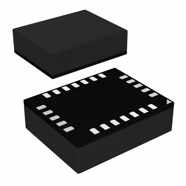
Small, 24-lead, 5 mm × 4 mm LGA package
Excellent ESD ratings
3500 V human body model (HBM)
1250 V field-induced charged device model (FICDM)
Wide operating temperature range: −55°C to +125°C
APPLICATIONS
LDO_OUT VDD
PD_REF
LDO
10µF
IN+
VIO
SDI
SCK
20Ω
IN–
PD_LDO
2.2µF
ADC
SDO
AMP_OUT
CNV
1.8nF
V– PD_AMP
ADAQ7980/
ADAQ7988
ADCN
GND
Figure 1.
The ADAQ7980/ADAQ7988 contain a high accuracy, low power,
16-bit SAR ADC, a low power, high bandwidth, high input
impedance ADC driver, a low power, stable reference buffer,
and an efficient power management block. Housed within a tiny,
5 mm × 4 mm LGA package, these products simplify the design
process for data acquisition systems. The level of system integration
of the ADAQ7980/ADAQ7988 solves many design challenges,
while the devices still provide the flexibility of a configurable
ADC driver feedback loop to allow gain and/or common-mode
adjustments. A set of four device supplies provides optimal system
performance; however, single-supply operation is possible with
minimal impact on device operating specifications.
The ADAQ7980/ADAQ7988 integrate within a compact,
integrated circuit (IC)-like form factor key components
commonly used in data acquisition signal chain designs. The
μModule family transfers the design burden of component
selection, optimization, and layout from designer to device,
shortening overall design time, system troubleshooting, and
ultimately improving time to market.
Automated test equipment (ATE)
Battery powered instrumentation
Communications
Data acquisition
Process control
Medical instruments
GENERAL DESCRIPTION
The ADAQ7980/ADAQ7988 are 16-bit analog-to-digital converter
(ADC) μModule® data acquisition systems that integrate four
common signal processing and conditioning blocks into a system
in package (SiP) design that supports a variety of applications.
These devices contain the most critical passive components,
eliminating many of the design challenges associated with
traditional signal chains that use successive approximation
register (SAR) ADCs. These passive components are crucial to
achieving the specified device performance.
Rev. A
V+ REF REF_OUT
15060-001
FEATURES
The serial peripheral interface (SPI)-compatible serial interface
features the ability to daisy-chain multiple devices on a single, 3wire bus and provides an optional busy indicator. The user
interface is compatible with 1.8 V, 2.5 V, 3 V, or 5 V logic.
Specified operation of these devices is from −55°C to +125°C.
Table 1. Integrated SAR ADC μModules
Type
16-Bit
500 kSPS
ADAQ7988
1000 kSPS
ADAQ7980
Document Feedback
Information furnished by Analog Devices is believed to be accurate and reliable. However, no
responsibility is assumed by Analog Devices for its use, nor for any infringements of patents or other
rights of third parties that may result from its use. Specifications subject to change without notice. No
license is granted by implication or otherwise under any patent or patent rights of Analog Devices.
Trademarks and registered trademarks are the property of their respective owners.
One Technology Way, P.O. Box 9106, Norwood, MA 02062-9106, U.S.A.
Tel: 781.329.4700
©2017 Analog Devices, Inc. All rights reserved.
Technical Support
www.analog.com
�ADAQ7980/ADAQ7988
Data Sheet
TABLE OF CONTENTS
Features .............................................................................................. 1
Slew Enhancement ..................................................................... 33
Applications ....................................................................................... 1
Effect of Feedback Resistor on Frequency Response ............ 33
General Description ......................................................................... 1
Voltage Reference Input ............................................................ 33
Functional Block Diagram .............................................................. 1
Power Supply............................................................................... 35
Revision History ............................................................................... 2
Specifications..................................................................................... 3
LDO Regulator Current-Limit and Thermal Overload
Protection .................................................................................... 36
Dual-Supply Configuration ........................................................ 3
LDO Regulator Thermal Considerations ............................... 36
Single-Supply Configuration ...................................................... 7
Digital Interface .......................................................................... 37
Timing Specifications ................................................................ 11
3-Wire CS Mode Without the Busy Indicator ........................ 38
Absolute Maximum Ratings .......................................................... 13
3-Wire CS Mode with the Busy Indicator ............................... 39
Thermal Data .............................................................................. 13
4-Wire CS Mode Without the Busy Indicator ........................ 40
Thermal Resistance .................................................................... 13
4-Wire CS Mode with the Busy Indicator ............................... 41
ESD Caution ................................................................................ 13
Chain Mode Without the Busy Indicator................................ 42
Pin Configuration and Function Descriptions ........................... 15
Chain Mode with the Busy Indicator ...................................... 43
Typical Performance Characteristics ........................................... 17
Application Circuits ....................................................................... 44
Terminology .................................................................................... 25
Nonunity Gain Configurations ................................................ 45
Theory of Operation ...................................................................... 26
Inverting Configuration with Level Shift ................................ 46
Circuit Information .................................................................... 26
Using the ADAQ7980/ADAQ7988 With Active Filters ........ 47
Converter Operation .................................................................. 26
Applications Information .............................................................. 48
Typical Connection Diagram.................................................... 27
Layout .......................................................................................... 48
ADC Driver Input ...................................................................... 28
Evaluating the Performance of the ADAQ7980/ADAQ7988 ... 48
Input Protection .......................................................................... 28
Outline Dimensions ....................................................................... 49
Noise Considerations And Signal Settling .............................. 28
Ordering Guide .......................................................................... 49
PD_AMP Operation .................................................................. 31
Dynamic Power Scaling (DPS) ................................................. 31
REVISION HISTORY
8/2017—Rev. 0 to Rev. A
Changed Integrated Data Acquisition System to μModule,
Subsystem to μModule Data Acquisition System, Subsystems to
μModule Data Acquisition Systems, and DAQ Subsystem to
μModule Data Acquisition System .............................. Throughout
Changes to Features Section and Table 1 Title ............................. 1
Moved General Description Section .............................................. 3
Changes to General Description Section ...................................... 3
Change to 0.1 Hz to 10 Hz Voltage Noise Parameter Heading,
Table 2 ................................................................................................ 4
Change to 0.1 Hz to 10 Hz Voltage Noise Parameter Heading,
Table 4 .................................................................................................8
Changes to Human Body Model (HBM) Parameter and
Endnote 4, Table 7 .......................................................................... 14
Change to Figure 27 Caption ........................................................ 21
Changes to Circuit Information Section ..................................... 27
Change to Table 15 Title ................................................................ 45
3/2017—Revision 0: Initial Version
Rev. A | Page 2 of 49
�ADAQ7980/ADAQ7988
Data Sheet
SPECIFICATIONS
DUAL-SUPPLY CONFIGURATION
VDD = 3.5 V to 10 V, V+ = 6.3 V to 7.7 V, V− = −2.5 V to −0.2 V, VIO = 1.7 V to 5.5 V, VREF = 5 V, TA = −55°C to +125°C, ADC driver in
a unity-gain buffer configuration, fSAMPLE = 1 MSPS (ADAQ7980), and fSAMPLE = 500 kSPS (ADAQ7988), unless otherwise noted.
Table 2.
Parameter
RESOLUTION
SYSTEM ACCURACY
No Missing Codes
Differential Nonlinearity Error (DNL)
Integral Nonlinearity Error (INL)
Transition Noise
Gain Error
Gain Error Temperature Drift
Zero Error
Zero Error Temperature Drift
Common-Mode Rejection Ratio
Power Supply Rejection Ratio
Positive
Negative
SYSTEM AC PERFORMANCE
Dynamic Range
Test Conditions/Comments
Min
16
16
−14
−20
Spurious-Free Dynamic Range
Total Harmonic Distortion (THD)
Signal-to-Noise-and-Distortion Ratio
Effective Number of Bits
Noise Free Code Resolution
SYSTEM SAMPLING DYNAMICS
Conversion Rate
ADAQ7980
ADAQ7988
Transient Response
−3 dB Input Bandwidth
−1 dB Frequency
−0.1 dB Frequency
0.1 Hz to 10 Hz Voltage Noise
Aperture Delay
Aperture Jitter
1
2
Max
+14
+20
Unit
Bits
Bits
ppm 1
ppm1
LSB1 rms
%FS
ppm/°C
mV
µV/°C
dB
TA = 25°C
−0.01
TA = 25°C
−0.5
ADC driver configured as difference amplifier
103
±7
±8
0.6
±0.002
0.1
±0.06
0.3
130
V+ = +6.3 V to +8 V, V− = −2 V
V+ = +7 V, V− = −1.0 V to −2.5 V
75
80
105
110
dB
dB
92
87
44.4
111
91.5
86.5
106
−105
91
86
14.8
14.1
dB 2
dB2
µV rms
dB2
dB2
dB2
dB2
dB2
dB2
dB2
Bits
Bits
VREF = 2.5 V
Total RMS Noise
Oversampled Dynamic Range
Signal-to-Noise Ratio (SNR)
Typ
Oversample dynamic range frequency (fODR) = 10 kSPS
Input frequency (fIN) = 10 kHz
fIN = 10 kHz, VREF = 2.5 V
fIN = 10 kHz
fIN = 10 kHz
fIN = 10 kHz
fIN = 10 kHz, VREF = 2.5 V
fIN = 10 kHz
VIO ≥ 3.0 V
VIO ≥ 1.7 V
VIO ≥ 1.7 V
Full-scale step
ADC driver RC filter
ADC driver RC filter
ADC driver RC filter
90.5
84.5
90
84
14.65
0
0
0
430
4.42
2.2
0.67
17
2.0
2.0
LSB means least significant bit. With the 5 V input range, 1 LSB is 76.3 µV and 1 LSB = 15.26 ppm.
All specifications in dB are referred to a full-scale input, FSR. Tested with an input signal at 0.5 dB below full scale, unless otherwise specified.
Rev. A | Page 3 of 49
+0.01
0.4
+0.5
1.3
−100
1
833
500
500
MSPS
kSPS
kSPS
ns
MHz
MHz
MHz
µV p-p
ns
ns
�ADAQ7980/ADAQ7988
Data Sheet
VDD = 3.5 V to 10 V, V+ = 6.3 V to 7.7 V, V− = −2.5 V to −0.2 V, VIO = 1.7 V to 5.5 V, VREF = 5 V, TA = −55°C to +125°C, ADC driver in
a unity-gain buffer configuration, and fSAMPLE = 1 MSPS (ADAQ7980) and fSAMPLE = 500 kSPS (ADAQ7988), unless otherwise noted.
Table 3.
Parameter
REFERENCE
Input Voltage Range
Load Current
Buffer Input
Resistance
Capacitance
Bias Current
Offset Voltage
Offset Voltage Drift
Voltage Noise
Voltage Noise 1/f Corner Frequency
Current Noise
0.1 Hz to 10 Hz Voltage Noise
Linear Output Current
Short-Circuit Current
ADC DRIVER CHARACTERISTICS
Voltage Range
Absolute Input Voltage
−3 dB Bandwidth
Bandwidth for 0.1 dB Flatness
Slew Rate
Input Voltage Noise
1/f Corner Frequency
0.1 Hz to 10 Hz Voltage Noise
Input Current
Noise
Bias
Offset
Input Offset Voltage
Drift
Open-Loop Gain
Input Resistance
Common Mode
Differential Mode
Input Capacitance
Input Common-Mode Voltage Range
Output Overdrive Recovery Time
Linear Output Current
Short-Circuit Current
DIGITAL INPUTS
Logic Levels
Input Voltage
Low (VIL)
High (VIH)
Test Conditions/Comments
Min
Voltage at REF pin
REFOUT
2.4
REF
REF
TA = 25°C
fIN = 100 kHz
fIN = 100 kHz
REFOUT
REFOUT sinking/sourcing
IN+, IN−, AMP_OUT
IN+, IN−, AMP_OUT
ADCN
G = +1, VAMP_OUT = 0.02 V p-p
G = +1, VAMP_OUT = 2 V p-p
G = +1, VAMP_OUT = 0.1 V p-p
G = +1, VAMP_OUT = 2 V step
G = +1, VAMP_OUT = 5 V step
f = 100 kHz
Typ
Max
Unit
5.1
330
V
µA
50
1
550
13
0.2
5.2
8
0.7
44
±40
85/73
MΩ
pF
nA
µV
µV/°C
nV/√Hz
Hz
pA/√Hz
nV rms
mA
mA
0
−0.1
−0.1
800
125
1.3
VREF
+5.1
+0.1
37
35
4
110
40
5.2
8
44
f = 100 kHz
IN+, IN−
0.7
550
2.1
13
0.2
111
TA = 25°C
800
125
1.3
V
V
V
MHz
MHz
MHz
V/µs
V/µs
nV/√Hz
Hz
nV rms
pA/√Hz
nA
nA
µV
µV/°C
dB
IN+, IN−
IN+, IN−
Specified performance
VIN+ = 10% overdrive, fIN = 10 kHz
50
260
1
−0.1
−0.3
−0.3
0.7 × VIO
0.9 × VIO
Rev. A | Page 4 of 49
+0.3 × VIO
+0.1 × VIO
VIO + 0.3
VIO + 0.3
V
V
V
V
500
±40
85/73
Sinking/sourcing
VIO > 3.0 V
VIO ≤ 3.0 V
VIO > 3.0 V
VIO ≤ 3.0 V
V+ − 1.3V
MΩ
kΩ
pF
V
ns
mA
mA
�Data Sheet
ADAQ7980/ADAQ7988
Parameter
Input Current
Low (IIL)
High (IIH)
DIGITAL OUTPUTS
Data Format
Pipeline Delay
Test Conditions/Comments
VOL
VOH
POWER-DOWN SIGNALING
ADC Driver/REF Buffer
PD_AMP, PD_REF Voltage
Low
High
Turn-Off Time
ISINK = 500 µA
ISOURCE = −500 µA
Turn-On Time
Dynamic Power Scaling Period
Low Dropout (LDO) Regulator
PD_LDO Voltage
Low
High
PD_LDO Logic Hysteresis
Turn-Off Time
Turn-On Time
POWER REQUIREMENTS
VDD
LDO Voltage Accuracy
LDO Line Regulation
LDO Load Regulation
LDO Start-Up Time
LDO Current-Limit Threshold
LDO Thermal Shutdown
Threshold
Hysteresis
LDO Dropout Voltage
V+
V−
VIO
Total Standby Current 1, 2
ADAQ7980 Current Draw
VIO
V+/V−
VDD
Min
Typ
−1
−1
10
Powered down
Enabled
1.06
1.15
2.2 µF capacitive load
3.5
−0.8
−1.8
TJ rising
ILDO_OUT = 10 mA
ILDO_OUT = 100 mA
3.7
V+ − 10
1.7
Rev. A | Page 5 of 49
+1
+1
µA
µA
V
V
2.6
1.25
2.75
2
7.25
µs
µs
1.12
1.22
100
460
370
1.18
1.30
650
425
V
V
mV
µs
µs
5
10
+0.8
+1.8
V
%
%
+0.015
0.004
460
%/V
%/mA
µs
mA
1.2
56
14
60
420
V− + 10
+0.1
5.5
1.7
103
23
°C
°C
mV
mV
V
V
V
mA
µA
µA
0.3
1.5
1.45
0.34
2.0
1.6
mA
mA
mA
−0.015
250
Static, all devices enabled
ADC driver, REF buffer disable
ADC driver, REF buffer, LDO disable
1 MSPS
Unit
Serial 16 bits, straight binary
Conversion results available
immediately after completed
conversion
0.4
VIO − 0.3
Powered down
Enabled
50% of PD_AMP, PD_REF to 3.0 V
VIO ≤ 3.0 V
VIO > 3.0 V
VIO ≤ 3.0 V
V+ − 1.3
MΩ
kΩ
pF
V
ns
mA
mA
�Data Sheet
ADAQ7980/ADAQ7988
Parameter
Input Current
Low (IIL)
High (IIH)
DIGITAL OUTPUTS
Data Format
Pipeline Delay
Test Conditions/Comments
VOL
VOH
POWER-DOWN SIGNALING
ADC Driver/Reference Buffer
PD_AMP, PD_REF Voltage
Low
High
Turn-Off Time
ISINK = 500 µA
ISOURCE = −500 µA
Turn-On Time
Dynamic Power Scaling Period
LDO
PD_LDO Voltage
Low
High
PD_LDO Logic Hysteresis
Turn-Off Time
Turn-On Time
POWER REQUIREMENTS
VDD
LDO Voltage Accuracy
LDO Line Regulation
LDO Load Regulation
LDO Start-Up Time
LDO Current-Limit Threshold
LDO Thermal Shutdown
Threshold
Hysteresis
LDO Dropout Voltage
V+
V−
VIO
Total Standby Current 1, 2
ADAQ7980 Current Draw
VIO
V+/V−
VDD
Min
Typ
−1
−1
Max
Unit
+1
+1
µA
µA
Serial 16 bits straight binary
Conversion results available
immediately after completed
conversion
0.4
VIO − 0.3
Powered down
Enabled
50% of PD_AMP, PD_REF to 3.0V, X = 70, AND Y = 30.
2 MINIMUM V AND MAXIMUM V USED. SEE DIGITAL INPUTS
IH
IL
SPECIFICATIONS IN TABLE 3 OR TABLE 5.
Figure 3. Voltage Levels for Timing
Rev. A | Page 12 of 49
15060-003
1
Symbol
tHSDO
tDSDO
�Data Sheet
ADAQ7980/ADAQ7988
ABSOLUTE MAXIMUM RATINGS
TA = 25°C, unless otherwise noted.
THERMAL RESISTANCE
Table 7.
Thermal resistance values specified in Table 8 were calculated
based on JEDEC specifications and must be used in compliance
with JESD51-12. Because the product contains more than one
silicon device, only the worst case junction temperature is reported.
Parameter
V+ to V−
V+ to GND
V− to GND
VDD to GND
REF_OUT/VIO to GND
IN+/IN−/REF to GND
AMP_OUT/ADCN to GND
Differential Analog Input Voltage
(IN+ − IN−)
Digital Input1 Voltage to GND
Digital Output2 Voltage to GND
Input Current to Any Pin Except Supplies3, 4
Operating Temperature Range
Storage Temperature Range
Junction Temperature
ESD
Human Body Model (HBM)
Field Induced Charged Device Model
(FICDM)
Rating
11 V
−0.3 V to +11 V
−11 V to +0.3 V
−0.3 V to +24 V
−0.3 V to +6 V
V− − 0.7 V to V+ + 0.7 V
−0.3 V to VREF + 0.3 V or
±130 mA
±1 V
−0.3 V to VIO + 0.3 V
−0.3 V to VIO + 0.3 V
±10 mA
−55°C to +125°C
−65°C to +150°C
150°C
3500 V
1250 V
The digital input pins include the following: CNV, SDI, and SCK.
The digital output pin is SDO.
3
Transient currents of up to 100 mA do not cause SCR latch-up.
4
Condition applies when power is provided to the device.
1
2
Table 8. Thermal Resistance
Package Type1, 2
CC-24-2
θJA
65
θJC TOP2
103
ΨJT
12.6
Unit
˚C/W
These values represent the worst case die junction in the package.
Table 8 values were calculated based on the standard JEDEC test conditions
defined in Table 9, unless otherwise specified.
3
For θJC test, 100 µm thermal interface material (TIM) was used. TIM is
assumed to be 3.6 W/mK.
1
2
Only use θJA and θJC TOP to compare thermal performance of the
package of the device with other semiconductor packages when
all test conditions listed are similar. One common mistake is to
use θJA and θJC to estimate the junction temperature in the system
environment. Instead, using ΨJT is a more appropriate way to
estimate the worst case junction temperature of the device in the
system environment. First, take an accurate thermal measurement
of the top center of the device (on the mold compound in this
case) while the device operates in the system environment. This
measurement is known in the following equation as TTOP. This
equation can then be used to solve for the worst case TJ in that
given environment as follows:
TJ = ΨJT × P + TTOP
Stresses at or above those listed under Absolute Maximum Ratings
may cause permanent damage to the product. This is a stress
rating only; functional operation of the product at these or any
other conditions above those indicated in the operational section of
this specification is not implied. Operation beyond the maximum
operating conditions for extended periods may affect product
reliability.
THERMAL DATA
where:
ΨJT is the junction to top thermal characterization number as
specified in data sheet.
P refers to total power dissipation in the chip (W).
TTOP refers to the package top temperature (°C) and is measured
at the top center of the package in the environment of the user.
ESD CAUTION
Absolute maximum ratings apply individually only, not in
combination. The ADAQ7980/ADAQ7988 can be damaged
when the junction temperature (TJ) limits are exceeded.
Monitoring ambient temperature does not guarantee that TJ is
within the specified temperature limits. In applications with
high power dissipation and poor thermal resistance, the
maximum ambient temperature (TA) may have to be derated.
In applications with moderate power dissipation and low printed
circuit board (PCB) thermal resistance, the maximum TA can
exceed the maximum limit as long as the junction temperature
is within specification limits. The θJA of the package is based on
modeling and calculation using a 4-layer board. The θJA is highly
dependent on the application and board layout. In applications
where high maximum power dissipation exists, close attention
to thermal board design is required. The θJA value may vary
depending on PCB material, layout, and environmental conditions.
Rev. A | Page 13 of 49
�ADAQ7980/ADAQ7988
Data Sheet
Table 9. Standard JEDEC Test Conditions
Test Conditions
Main Heat Transfer Mode
Board Type
Board Thickness
Board Dimension
Signal Traces Thickness
PWR/GND Traces Thickness
Thermal Vias
Cold Plate
θJA
Convection
2S2P
1.6 mm
If package length is