Rail-to-Rail, Very Fast, 2.5 V to 5.5 V, Single-Supply CML Comparators ADCMP606/ADCMP607
FEATURES
Fully specified rail to rail at VCCI = 2.5 V to 5.5 V Input common-mode voltage from −0.2 V to VCCI + 0.2 V CML-compatible output stage 1.25 ns propagation delay 50 mW @ 2.5 V power supply Shutdown pin Single-pin control for programmable hysteresis and latch (ADCMP607 only) Power supply rejection > 60 dB −40°C to +125°C operation
GENERAL DESCRIPTION
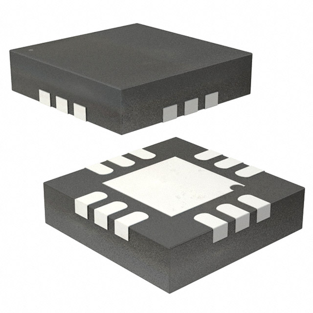
The ADCMP606 and ADCMP607 are very fast comparators fabricated on XFCB2, an Analog Devices, Inc., proprietary process. These comparators are exceptionally versatile and easy to use. Features include an input range from VEE − 0.5 V to VCCI + 0.2 V, low noise, CML-compatible output drivers, and TTL-/CMOS-compatible latch inputs with adjustable hysteresis and/or shutdown inputs. The devices offer 1.25 ns propagation delay with 2.5 ps rms random jitter (RJ). Overdrive and slew rate dispersion are typically less than 50 ps. A flexible power supply scheme allows the devices to operate with a single +2.5 V positive supply and a −0.5 V to +2.7 V input signal range up to a +5.5 V positive supply with a −0.5 V to +5.7 V input signal range. The ADCMP607 features split input/output supplies with no sequencing restrictions to support a wide input signal range with independent output swing control and power savings. The CML-compatible output stage is fully back-matched for superior performance. The comparator input stage offers robust protection against large input overdrive, and the outputs do not phase reverse when the valid input signal range is exceeded. On the ADCMP607, latch and programmable hysteresis features are also provided with a unique single-pin control option. The ADCMP606 is available in a 6-lead SC70 package and the ADCMP607 is available in a 12-lead LFCSP package.
APPLICATIONS
High speed instrumentation Clock and data signal restoration Logic level shifting or translation Pulse spectroscopy High speed line receivers Threshold detection Peak and zero-crossing detectors High speed trigger circuitry Pulse-width modulators Current-/voltage-controlled oscillators Automatic test equipment (ATE)
FUNCTIONAL BLOCK DIAGRAM
VCCI VCCO (ADCMP607 ONLY)
VP NONINVERTING INPUT
Q OUTPUT
ADCMP606/ ADCMP607
VN INVERTING INPUT
CML Q OUTPUT
LE/HYS INPUT (ADCMP607 ONLY) SDN INPUT (ADCMP607 ONLY)
Figure 1.
Rev. A
Information furnished by Analog Devices is believed to be accurate and reliable. However, no responsibility is assumed by Analog Devices for its use, nor for any infringements of patents or other rights of third parties that may result from its use. Specifications subject to change without notice. No license is granted by implication or otherwise under any patent or patent rights of Analog Devices. Trademarks and registered trademarks are the property of their respective owners.
One Technology Way, P.O. Box 9106, Norwood, MA 02062-9106, U.S.A. Tel: 781.329.4700 www.analog.com Fax: 781.461.3113 ©2006–2007 Analog Devices, Inc. All rights reserved.
05917-001
�ADCMP606/ADCMP607 TABLE OF CONTENTS
Features .............................................................................................. 1 Applications....................................................................................... 1 General Description ......................................................................... 1 Functional Block Diagram .............................................................. 1 Revision History ............................................................................... 2 Specifications..................................................................................... 3 Electrical Characteristics............................................................. 3 Timing Information ..................................................................... 5 Absolute Maximum Ratings............................................................ 6 Thermal Resistance ...................................................................... 6 ESD Caution.................................................................................. 6 Pin Configurations and Function Descriptions ........................... 7 Typical Performance Characteristics ............................................. 8 Application Information................................................................ 10 Power/Ground Layout and Bypassing..................................... 10 CML-Compatible Output Stage ............................................... 10 Using/Disabling the Latch Feature........................................... 10 Optimizing Performance........................................................... 10 Comparator Propagation Delay Dispersion ........................... 11 Comparator Hysteresis .............................................................. 11 Crossover Bias Points................................................................. 12 Minimum Input Slew Rate Requirement ................................ 12 Typical Application Circuits ......................................................... 13 Outline Dimensions ....................................................................... 14 Ordering Guide .......................................................................... 14
REVISION HISTORY
8/07—Rev. 0 to Rev. A Changes to Specifications Section.................................................. 3 Changes to Table 3............................................................................ 6 Changes to Ordering Guide .......................................................... 14 10/06—Revision 0: Initial Version
Rev. A | Page 2 of 16
�ADCMP606/ADCMP607 SPECIFICATIONS
ELECTRICAL CHARACTERISTICS
VCCI = VCCO = 2.5 V, TA = −40°C to +125°C, typical at TA = 25°C, unless otherwise noted. Table 1.
Parameter DC INPUT CHARACTERISTICS Voltage Range Common-Mode Range Differential Voltage Offset Voltage Bias Current Offset Current Capacitance Resistance, Differential Mode Resistance, Common Mode Active Gain Common-Mode Rejection Ratio Symbol VP, VN Conditions VCCI = 2.5 V to 5.5 V VCCI = 2.5 V to 5.5 V VCCI = 2.5 V to 5.5 V Min −0.5 −0.2 −5.0 −5.0 −2.0 −0.1 V to VCCI −0.5 V to VCCI + 0.5 V AV CMRR VCCI = 2.5 V, VCCO = 2.5 V, VCM = −0.2 V to +2.7 V VCCI = 2..5 V, VCCO = 5.5 V RHYS = ∞ 200 100 50 50
很抱歉,暂时无法提供与“ADCMP607BCPZ-WP”相匹配的价格&库存,您可以联系我们找货
免费人工找货