-..
W
HighResolution
16-Bit0/A Converters
ANALOG
DEVICES
ADoAC71/AoDAC72*
I
FEATURES
16-Bit Resolution
j: 0.003% Maximum Nonlinearity
Low Gain Drift j: 7ppm/oC
0 to + 70°C Operation (AD DAC71, AD DAC71H,
AD DAC72C)
- 25°C to + 85°C Operation (AD DAC72)
Current and Voltage Models Available
Improved Second-Source
Low Cost
AD DAC71/AD DAC 72 FUNCTIONAL
BLOCK DIAGRAM
.
if1
OBS
OLE
SUMMING JUNCTION
BIT 9
AD DAC71/AD
PRODUCT DESCRIPTION
The AD DAC71 and AD DACn are high resolution 16-bit
hybrid IC digital-to-analog converters including reference, scaling
resistors and output amplifier (V models).
The devices offer outstanding accuracy, including maximum
linearity error of 0.003% at room temperature and maximum
gain drifts of 15ppmrC (AD DAC71, AD DAC7IH, AD DACnC)
and 7ppm/°C (AD DACn). This performance is possible due to
the innovative design, using proprietary monolithic D/A converter
chips. Laser-trimmed thin fllm resistors provide the linearity
and wide temperature range for guaranteed monotonicity.
TE
DAC72
PRODUCT HIGHLIGHTS
1. The AD DAC7l and AD DACn
with 0.003% linearity error.
provide l6-bit resolution
2. The proprietary chips used in the hybrid design provide
excellent stability over temperature and improved reliability.
3. Unipolar and bipolar current and voltage output versions are
available to fill a wide range of system requirements.
4. The AD DAC71 and AD DACn are improved second source
replacements for DAC71 and DACn devices from other
manufacturers.
The AD DAC71 and AD DACn digital inputs are ITL-compatible. Coding is complementary straight binary (CSB) for
unipolar output versions and complementary offset binary (COB)
for bipolar output versions.
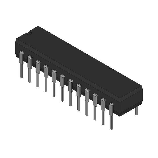
All versions are packaged in a 24-pin metal DIP. The AD DAC71,
AD DAC71H and AD DACnC are specified for operation from
0 to + 70°C, and the AD DACn is specified from - 25°C to
+ 85°C. The AD DAC7IH, AD DACn and AD DACnC are
supplied in hermetically-sealed packages.
The AD DAC71 and AD DACn are intended to serve as improved
second sources to DAC71 and DACn devices from other
manufacturers.
*Covered by Patent Numbers: 3,978,473; RE28,633;
3,803,590; 3,961,326; 4,213,806; 4,136,349.
4,020,486;
3,747,088;
~ ~-~~
�SPECIFICATIONS
(@ TA =
AD DAC71/AD DAC71H
MIN
TYP
MAX
MODEL
DIGITAL INPUTS
Resolution
Logic Levels (TTL-Compatible)t
Logical "I"
Logical "0"
+ 25°C,ratedpowersuppliesunlessotherwise
noted)
MIN
AD DAC72C
TYP
MAX
16
MIN
AD DAC72
TYP
MAX
16
+ 2.4
+0
+5.5
+0.4
UNITS
16
+2.4
+0
+ 5.5
+0.4
Birs
+2.4
+0
+5.5
+0.4
Vdc
Vdc
=0.003
=0.15
=0.25
=2.0
= 10.0
= 1.0
=5.0
+70
% ofFSR3
%
%
mV
mV
'" 19
",II
ppmofFSRI'C
ppmofFSRI'C
ACCURACY'
Linearity Error at 2S'C
Gain Error', Voltage
Current
Offset Error" Voltage, Unipolar
Voltage, Bipolar
Current, Unipolar
Current, Bipolar
MonotonicilY Temp. Range (14-Birs)
000.003
=0.1
=0.25
=2.0
=5.0
= 1.0
=5.0
+50
=0.01
=0.05
=0.1
o
=0.003
=0.15
=0.25
'" 2.0
= 10.0
= 1.0
=5.0
+50
=0.05
=0.05
=0.1
o
=0.05
=0.05
",0.1
o
flA
flA
'C
DRIFT (Over Specified Temp. Range)
Total Bipolar Drift (includes gain, offset,
and linearity drifl)
Voltage
",7
'1'min to 2S'C
= IS
= IS
=7
25'CtoTmu
Current
OBS
+15
TmintoTmu
",7
'" IS
=7
'" 15
=5
=5
+ IS
+10
ppmofFSRI'C
TOTAL ERROR OVER TEMP. RANGEs
Voltage, Unipolar
Tminto+2S'C
+2S'CtoTmu
Voltage, Bipolar
TminlO +2S'C
+2S'CtoTmu
Current, Unipolar ('1'mlnto '1'mu)
Bipolar ('1'mintoT mu)
",0.083
= 0.083
"'°.083
= 0.083
",0.100
",0.072
%ofFSR
%ofFSR
",0.071
",0.071
=0.23
=0.23
'" 0.071
=0.071
=0.23
",0.23
=0.100
",0.072
=0.24
",0.24
%ofFSR
%ofFSR
%ofFSR
%ofFSR
'" IS
'" 15
= 15
",IS
= 15
",7
TEMPERATURE COEFFICIENTS
Gain
Voltage
TminlO +2S'C
+ 2S'C to '1'mu
Current
Offset
'" IS
= IS
=2
"'I
Voltage, Unipolar
Bipolar
Currenl, Unipolar
Bipolar
Differential LinearilY over Temperalure
Linearity Error over Temperalure
OLE
"'1
= 10
",I
= 15
",10
=2
"'1
=10
",I
=8
",1
",15
",2
",2
=2
"'10
=2
=2
=I
",1
SETTLING TIME
Vollage Models(lo '" 0.003% ofFSR)
Output: 20V Step
ILSB Step'
Slew Rate
5
3
20
Current Models (to '" 0.003% ofFSR)7
Output: 2mA step IOn to loon Load
Ikn Load
Switching Transienl
10
5
5
3
20
1
3
10
5
5
3
20
I
3
10
5
I
3
500
500
500
010 11O
c'c1O
010 , 10
,,10
Oto.. 10
'10
TE
ppmofFSRI'C
ppmofFSRI'C
ppmofFSRI'C
ppm ofFSRI'C
ppmofFSRI'C
ppmofFSRI'C
ppmofFSRI'C
ppmofFSRI'C
ppm ofFSRI'C
flS
flS
VlflS
flS
flS
mV
ANALOG OUTPUT
Voltage Models
Ranges-CSB
COB
Output Currenl
OUIPUIImpedance (de)
Short Circuit Duralion
Current Models
5
Ranges-CSB
COB
OutPUI Impedance-Unipnlar
Bipolar
Compliance
INTERNAL REFERENCE VOLTAGE
Maximum External Current'
Temp. Coeff. of Drift
POWER SUPPLY SENSITIVITY
lJnipnlarOffset
= ISVdc
I 5Vdc
Bipolar Offsot
.IWdc
I 5V de
c'c5
0.05
Indefinite 10Common
010
'I
6.0
3.0
6.0
,]0
6.3
6.6
,3
',1O
5
0.05
IndefinilclnCommon
0.05
Indefinite In Common
()10 2
'I
6.0
3.0
Oto - 2
2
].5
IS
6.0
V
V
mA
"I
6.0
3.0
I ]0
6.3
0.0001
6.6
'3
'10
IS
6.()
, ]0
6.3
6.6
3
,,5
n
mA
mA
kn
kn
V
V
mA
nnml"C
().0001
,0.0001
+
'O.()()o1
',0.000]
'O.()()()]
%nfFSRI%V,
%ofFSR/%V,
. O.0004
'. 0.Q()()4
,O.Q(XJI
'O.00()4
'().OOOI
%nfFSR/% V,
% of FSRI% V,
'"O.()()()]
2-306 DIGITAL-TO-ANALOG CONVERTERS
�AD DAC71/AD DAC71H
MAX
TYI'
MIN
MODEL
POWER SUPPLY SENSITIVITY
(Contmued)
Gaio
, 1SVde
I SVde
POWER SUPPLY REQUIREMENTS
DAC71172
.
Dram.
TEMPERATURE
0.001
+
+ 14.5.
+ 15.0.
I 5.0
10
I 1SV de (no load)
AD DAC72
MAX
Tn
MIN
0.001
.,0.001
,,0.0005
. 0.0001
, 0.0005
I 4.75
Supply
AD DAC72C
MAX
TYI'
MIN
. 145.
'15.5.
I 5.25
. 15.0.
+ 4.75
10
20
'.15.5.
15.0
! 14.5.
+ 4.75
15.25
,15.0.
I 5.0
20
10
UNITS
.
%ofFSR/%V,
%ofFSR/% Vs
'15.5.
I 5.25
20
Vde
rnA
15Vdc(noload)
30
55
30
55
30
55
mA
I 5Vde(loglcsupply)
10
20
10
20
10
20
lOA
185
+ 100
; 110
"C
"C
"C
RANGE
Specification
Operating (double above Drift Specs)
Storage
0
25
. 55
0
I 70
185
+ 100
25
. 55
OBS
25
55
55
I 70
t 85
+ 100
NOTES
'Adding
