High Performance
Narrow-Band Transceiver IC
ADF7021
Data Sheet
FEATURES
On-chip VCO and fractional-N PLL
On-chip, 7-bit ADC and temperature sensor
Fully automatic frequency control loop (AFC)
Digital received signal strength indication (RSSI)
Integrated Tx/Rx switch
0.1 μA leakage current in power-down mode
Low power, narrow-band transceiver
Frequency bands using dual VCO
80 MHz to 650 MHz
862 MHz to 950 MHz
Modulation schemes
2FSK, 3FSK, 4FSK, MSK
Spectral shaping
Gaussian and raised cosine filtering
Data rates supported
0.05 kbps to 32.8 kbps
2.3 V to 3.6 V power supply
Programmable output power
−16 dBm to +13 dBm in 63 steps
Automatic PA ramp control
Receiver sensitivity
−130 dBm at 100 bps, 2FSK
−122 dBm at 1 kbps, 2FSK
−113 dBm at 25 kbps, raised cosine 2FSK
Patent pending, on-chip image rejection calibration
APPLICATIONS
Narrow-band standards
ETSI EN 300 220, FCC Part 15, FCC Part 90, FCC Part 95,
ARIB STD-T67
Low cost, wireless data transfer
Remote control/security systems
Wireless metering
Private mobile radio
Wireless medical telemetry service (WMTS)
Keyless entry
Home automation
Process and building control
Pagers
FUNCTIONAL BLOCK DIAGRAM
CE
RSET
TEMP
SENSOR
RLNA
MUX
7-BIT ADC
2FSK
3FSK
4FSK
LNA
RFIN
RSSI/
LOG AMP
IF FILTER
RFINB
CREG(1:4)
MUXOUT
LDO(1:4)
TEST MUX
CLOCK
AND DATA
RECOVERY
DEMODULATOR
TxRxCLK
Tx/Rx
CONTROL
TxRxDATA
SWD
GAIN
AGC
CONTROL
SLE
SERIAL
PORT
AFC
CONTROL
PA RAMP
DIV P
÷1/÷2
VCO1
VCO2
VCOIN
SCLK
GAUSSIAN/
RAISED COSINE
FILTER
3FSK
ENCODING
CP
PFD
DIV R
L2
2FSK
3FSK
4FSK
MOD CONTROL
Σ-∆
MODULATOR
÷2
MUX
L1
N/N + 1
SREAD
CPOUT
CLK
DIV
OSC
OSC1
OSC2
CLKOUT
05876-001
RFOUT
SDATA
Figure 1.
Rev. D
Document Feedback
Information furnished by Analog Devices is believed to be accurate and reliable. However, no
responsibility is assumed by Analog Devices for its use, nor for any infringements of patents or other
rights of third parties that may result from its use. Specifications subject to change without notice. No
license is granted by implication or otherwise under any patent or patent rights of Analog Devices.
Trademarks and registered trademarks are the property of their respective owners.
One Technology Way, P.O. Box 9106, Norwood, MA 02062-9106, U.S.A.
Tel: 781.329.4700 ©2007–2016 Analog Devices, Inc. All rights reserved.
Technical Support
www.analog.com
�ADF7021
Data Sheet
TABLE OF CONTENTS
Features .............................................................................................. 1
Receiver Setup ............................................................................. 34
Applications ....................................................................................... 1
Demodulator Considerations ................................................... 36
Functional Block Diagram .............................................................. 1
AFC Operation ........................................................................... 36
Revision History ............................................................................... 3
Automatic Sync Word Detection (SWD) ................................ 37
General Description ......................................................................... 4
Applications Information .............................................................. 38
Specifications..................................................................................... 5
IF Filter Bandwidth Calibration ............................................... 38
RF and PLL Specifications........................................................... 5
LNA/PA Matching ...................................................................... 38
Transmission Specifications ........................................................ 6
Image Rejection Calibration ..................................................... 39
Receiver Specifications ................................................................ 8
Packet Structure and Coding .................................................... 41
Digital Specifications ................................................................. 10
Applications Circuit ................................................................... 44
General Specifications ............................................................... 11
Serial Interface ................................................................................ 45
Timing Characteristics .............................................................. 11
Readback Format........................................................................ 45
Absolute Maximum Ratings .......................................................... 15
Interfacing to Microcontroller/DSP ........................................ 46
ESD Caution ................................................................................ 15
Register 0—N Register............................................................... 47
Pin Configuration and Function Descriptions ........................... 16
Register 1—VCO/Oscillator Register ...................................... 47
Typical Performance Characteristics ........................................... 18
Register 2—Transmit Modulation Register ............................ 49
Frequency Synthesizer ................................................................... 22
Register 3—Transmit/Receive Clock Register ........................ 50
Reference Input ........................................................................... 22
Register 4—Demodulator Setup Register ............................... 51
MUXOUT.................................................................................... 23
Register 5—IF Filter Setup Register......................................... 52
Voltage Controlled Oscillator (VCO) ...................................... 24
Register 6—IF Fine Cal Setup Register ................................... 53
Choosing Channels for Best System Performance ................. 25
Register 7—Readback Setup Register ...................................... 54
Transmitter ...................................................................................... 26
Register 8—Power-Down Test Register .................................. 55
RF Output Stage .......................................................................... 26
Register 9—AGC Register ......................................................... 56
Modulation Schemes.................................................................. 26
Register 10—AFC Register ....................................................... 57
Spectral Shaping ......................................................................... 28
Register 11—Sync Word Detect Register ................................ 58
Modulation and Filtering Options ........................................... 29
Register 12—SWD/Threshold Setup Register ........................ 58
Transmit Latency ........................................................................ 29
Register 13—3FSK/4FSK Demod Register ............................. 59
Test Pattern Generator ............................................................... 29
Register 14—Test DAC Register ............................................... 60
Receiver Section .............................................................................. 30
Register 15—Test Mode Register ............................................. 61
RF Front End ............................................................................... 30
Outline Dimensions ....................................................................... 62
IF Filter ........................................................................................ 30
Ordering Guide .......................................................................... 62
RSSI/AGC .................................................................................... 31
Demodulation, Detection, and CDR ....................................... 32
Rev. D | Page 2 of 62
�Data Sheet
ADF7021
REVISION HISTORY
9/2016—Rev. C to Rev. D
Changes to General Description Section ....................................... 4
Changes to Interfacing to Microcontroller/DSP Section and
Figure 58 ...........................................................................................46
10/2014—Rev. B to Rev. C
Changes to Table 8 ..........................................................................16
Change to Figure 36 ........................................................................24
Change to IF Filter Fine Calibration Overview Section ............30
Change to Post Demodulator Filter Setup Section .....................34
Change to Battery Voltage/ADCIN/Temperature Sensor
Readback Section ............................................................................45
Change to Register 4—Demodulator Setup Register Section ...51
Change to Register 7—Readback Setup Register Section ..........54
Change to Register 10—AFC Register Section ...........................57
4/2013—Rev. A to Rev. B
Changes to Figure 10 ......................................................................16
Updated Outline Dimensions ........................................................62
Changes to Ordering Guide ...........................................................62
9/2007—Rev. 0 to Rev. A
Change to UART/SPI Mode Section ............................................ 14
Changes to Figure 10 ...................................................................... 16
Change to Table 8 ............................................................................ 16
Changes to Figure 12 ...................................................................... 18
Change to Internal Inductor VCO Section.................................. 24
Changes to Figure 40 ...................................................................... 26
Changes to Figure 47 ...................................................................... 32
Change to Table 19 .......................................................................... 34
Changes to Figure 56 ...................................................................... 44
Change to SPI Mode Section ......................................................... 46
Changes to Figure 59 ...................................................................... 46
Changes to Figure 60 ...................................................................... 46
Change to Register 3—Transmit/Receive Clock
Register Section ............................................................................... 50
Change to Register 4—Demodulator Setup Register Section ......... 51
Change to Register 7—Readback Setup Register ........................ 54
Change to Register 13—3FSK/4FSK Demod Register Heading .... 59
3/2007—Revision 0: Initial Version
Rev. D | Page 3 of 62
�ADF7021
Data Sheet
GENERAL DESCRIPTION
The ADF7021 is a high performance, low power, highly integrated
2FSK/3FSK/4FSK transceiver. It is designed to operate in the
narrowband, license-free ISM bands, and in the licensed bands
with frequency ranges of 80 MHz to 650 MHz and 862 MHz to
950 MHz. The device has both Gaussian and raised cosine transmit
data filtering options to improve spectral efficiency for narrowband applications. It is suitable for circuit applications targeted
at European ETSI EN 300 220, the Japanese ARIB STD-T67, the
Chinese short range device regulations, and the North American
FCC Part 15, Part 90, and Part 95 regulatory standards. A complete
transceiver can be built using a small number of external discrete
components, making the ADF7021 very suitable for price
sensitive and area sensitive applications.
The range of on-chip FSK modulation and data filtering options
allows users greater flexibility in their choice of modulation
schemes while meeting tight spectral efficiency requirements.
The ADF7021 also supports protocols that dynamically switch
between 2FSK/3FSK/4FSK to maximize communication range
and data throughput.
The transmit section contains dual voltage controlled oscillators
(VCOs) and a low noise fractional-N PLL with an output resolution
of 10
>10
>25
>25
>10
>20
5
>5
>¼ × tBIT
>¼ × tBIT
Unit
ns
ns
ns
ns
ns
ns
ns
ns
ns
ns
ns
ns
µs
µs
Test Conditions/Comments
SDATA to SCLK setup time
SDATA to SCLK hold time
SCLK high duration
SCLK low duration
SCLK to SLE setup time
SLE pulse width
SCLK to SREAD data valid, readback
SREAD hold time after SCLK, readback
SCLK to SLE disable time, readback
TxRxCLK negative edge to SLE
TxRxDATA to TxRxCLK setup time (Tx mode)
TxRxCLK to TxRxDATA hold time (Tx mode)
TxRxCLK negative edge to SLE
SLE positive edge to positive edge of TxRxCLK
Rev. D | Page 11 of 62
�ADF7021
Data Sheet
Timing Diagrams
Serial Interface
t3
t4
SCLK
t1
SDATA
DB31 (MSB)
t2
DB30
DB1
(CONTROL BIT C2)
DB2
DB0 (LSB)
(CONTROL BIT C1)
t6
05876-002
SLE
t5
Figure 2. Serial Interface Timing Diagram
t1
t2
SCLK
SDATA
REG7 DB0
(CONTROL BIT C1)
SLE
t3
t10
RV16
RV2
RV15
RV1
X
05876-003
X
SREAD
t9
t8
Figure 3. Serial Interface Readback Timing Diagram
2FSK/3FSK Timing
±1 × DATA RATE/32
1/DATA RATE
TxRxCLK
TxRxDATA
05876-004
DATA
Figure 4. TxRxDATA/TxRxCLK Timing Diagram in Receive Mode
1/DATA RATE
TxRxCLK
TxRxDATA
FETCH
05876-005
DATA
SAMPLE
Figure 5. TxRxDATA/TxRxCLK Timing Diagram in Transmit Mode
Rev. D | Page 12 of 62
�Data Sheet
ADF7021
4FSK Timing
In 4FSK receive mode, MSB/LSB synchronization is guaranteed by SWD in the receive bit stream.
REGISTER 0 WRITE
SWITCH FROM Rx TO Tx
tSYMBOL
t13
t12
t11
tBIT
SLE
TxRxCLK
Rx SYMBOL
MSB
Rx SYMBOL
LSB
Tx/Rx MODE
Rx SYMBOL
MSB
Rx SYMBOL
LSB
Tx SYMBOL
MSB
Tx SYMBOL
LSB
Rx MODE
Tx SYMBOL
MSB
Tx MODE
05876-074
TxRxDATA
Figure 6. Receive-to-Transmit Timing Diagram in 4FSK Mode
REGISTER 0 WRITE
SWITCH FROM Tx TO Rx
t15
t14
tSYMBOL
tBIT
SLE
TxRxCLK
Tx/Rx MODE
Tx SYMBOL
MSB
Tx SYMBOL
LSB
Tx SYMBOL
MSB
Tx SYMBOL
LSB
Tx MODE
Figure 7. Transmit-to-Receive Timing Diagram in 4FSK Mode
Rev. D | Page 13 of 62
Rx SYMBOL
MSB
Rx SYMBOL
LSB
Rx MODE
05876-075
TxRxDATA
�ADF7021
Data Sheet
UART/SPI Mode
UART mode is enabled by setting R0_DB28 to 1. SPI mode is enabled by setting R0_DB28 to 1 and setting R15_DB[17:19] to 0x7.
The transmit/receive data clock is available on the CLKOUT pin.
tBIT
CLKOUT
(TRANSMIT/RECEIVE DATA
CLOCK IN SPI MODE.
NOT USED IN UART MODE.)
Tx BIT
SAMPLE
Tx BIT
TxRxDATA
(RECEIVE DATA OUTPUT
IN UART/SPI MODE.)
Tx BIT
Tx BIT
Tx BIT
HIGH-Z
Tx/Rx MODE
05876-082
TxRxCLK
(TRANSMIT DATA INPUT
IN UART/SPI MODE.)
FETCH
Tx MODE
Figure 8. Transmit Timing Diagram in UART/SPI Mode
tBIT
CLKOUT
(TRANSMIT/RECEIVE DATA
CLOCK IN SPI MODE.
NOT USED IN UART MODE.)
FETCH SAMPLE
TxRxCLK
(TRANSMIT DATA INPUT
IN UART/SPI MODE.)
Tx/Rx MODE
Rx BIT
Rx BIT
Rx BIT
Rx BIT
Rx MODE
Figure 9. Receive Timing Diagram in UART/SPI Mode
Rev. D | Page 14 of 62
Rx BIT
05876-078
TxRxDATA
(RECEIVE DATA OUTPUT
IN UART/SPI MODE.)
HIGH-Z
�Data Sheet
ADF7021
ABSOLUTE MAXIMUM RATINGS
TA = 25°C, unless otherwise noted.
Table 7.
Parameter
VDD to GND1
Analog I/O Voltage to GND
Digital I/O Voltage to GND
Operating Temperature Range
Industrial (B Version)
Storage Temperature Range
Maximum Junction Temperature
MLF θJA Thermal Impedance
Reflow Soldering
Peak Temperature
Time at Peak Temperature
1
Rating
−0.3 V to +5 V
−0.3 V to AVDD + 0.3 V
−0.3 V to DVDD + 0.3 V
−40°C to +85°C
−65°C to +125°C
150°C
26°C/W
260°C
40 sec
Stresses at or above those listed under Absolute Maximum
Ratings may cause permanent damage to the product. This is a
stress rating only; functional operation of the product at these
or any other conditions above those indicated in the operational
section of this specification is not implied. Operation beyond
the maximum operating conditions for extended periods may
affect product reliability.
This device is a high performance RF integrated circuit with an
ESD rating of 10 ppm
tolerance, but to comply with the absolute frequency error
specifications of narrow-band regulations (for example, ARIB
STD-T67 and ETSI EN 300-220), compensation for the
frequency error of the crystal is necessary.
The CLKOUT circuit takes the reference clock signal from the
oscillator section, shown in Figure 32, and supplies a divideddown, 50:50 mark-space signal to the CLKOUT pin. The CLKOUT
signal is inverted with respect to the reference clock. An even
divide from 2 to 30 is available. This divide number is set in
R1_DB[7:10]. On power-up, the CLKOUT defaults to divide-by-8.
DVDD
CLKOUT
ENABLE BIT
05876-083
CP1
Two parallel resonant capacitors are required for oscillation at
the correct frequency. Their values are dependent upon the
crystal specification. When choosing the values of the capacitors,
make sure that the series value of capacitance added to the PCB
track capacitance adds up to the specified load capacitance of the
crystal, usually 12 pF to 20 pF. Track capacitance values vary
from 2 pF to 5 pF, depending on board layout. When possible,
choose capacitors that have a very low temperature coefficient
to ensure stable frequency operation over all conditions.
Using a TCXO Reference
A single-ended reference (TCXO, VCXO, or OCXO) can also be
used with the ADF7021. This is recommended for applications
having absolute frequency accuracy requirements of 6 and KP < 7
The recommended settings to give optimal AFC performance
are KI = 11 and KP = 4.
To tradeoff between AFC settling time and AFC accuracy, the
KI and KP parameters can be adjusted from the recommended
settings (staying within the allowable range) such that
Signals that are within the AFC pull-in range but outside the IF
filter bandwidth are attenuated by the IF filter. As a result, the
signal can be below the sensitivity point of the receiver and,
therefore, not detectable by the AFC.
Rev. D | Page 57 of 62
�ADF7021
Data Sheet
DB5
DB4
DB3
DB2
DB1
DB0
PL1
C4 (1)
C3 (0)
C2 (1)
C1 (1)
DB9
SB2
CONTROL
BITS
PL2
MATCHING_
TOLERANCE
DB10
SB3
DB6
DB11
SB4
MT1
DB12
SB5
DB7
DB13
SB6
DB8
DB14
SB7
SB1
DB15
SB8
MT2
DB16
SB9
SB10 DB17
SB11 DB18
SB12 DB19
SB13 DB20
SB14 DB21
SB15 DB22
SB16 DB23
SB17 DB24
SB18 DB25
SB19 DB26
SB20 DB27
SB21 DB28
SB22 DB29
SB23 DB30
SYNC_BYTE_SEQUENCE
SB24 DB31
SYNC_BYTE_
LENGTH
REGISTER 11—SYNC WORD DETECT REGISTER
PL2
PL1
SYNC BYTE
LENGTH
0
0
1
1
0
1
0
1
12 BITS
16 BITS
20 BITS
24 BITS
0
0
1
1
0
1
0
1
ACCEPT 0 ERRORS
ACCEPT 1 ERROR
ACCEPT 2 ERRORS
ACCEPT 3 ERRORS
05876-041
MATCHING
MT2 MT1 TOLERANCE
Figure 73. Register 11—Sync Word Detect Register Map
SWD_MODE
LOCK_
THRESHOLD_
MODE
REGISTER 12—SWD/THRESHOLD SETUP REGISTER
DB15
DB14
DB13
DB12
DB11
DB10
DB9
DB8
DB7
DB6
DB5
DB4
DB3
DB2
DB1
DB0
DP7
DP6
DP5
DP4
DP3
DP2
DP1
IL2
IL1
LM2
LM1
C4 (1)
C3 (1)
C2 (0)
C1 (0)
CONTROL
BITS
DP8
DATA_PACKET_LENGTH
DATA PACKET LENGTH
0
1
...
255
INVALID
1 BYTE
...
255 BYTES
SWD MODE
0
1
2
3
SWD PIN LOW
SWD PIN HIGH AFTER NEXT SYNCWORD
SWD PIN HIGH AFTER NEXT SYNCWORD
FOR DATA PACKET LENGTH NUMBER OF BYTES
INTERRUPT PIN HIGH
3
THRESHOLD FREE RUNNING
LOCK THRESHOLD AFTER NEXT SYNCWORD
LOCK THRESHOLD AFTER NEXT SYNCWORD
FOR DATA PACKET LENGTH NUMBER OF BYTES
LOCK THRESHOLD
05876-042
LOCK THRESHOLD MODE
0
1
2
Figure 74. Register 12—SWD/Threshold Setup Register Map
Lock threshold locks the threshold of the envelope detector. This has the effect of locking the slicer in linear demodulation and locking
the AFC and AGC loops when using linear or correlator demodulation.
Rev. D | Page 58 of 62
�Data Sheet
ADF7021
REGISTER 13—3FSK/4FSK DEMOD REGISTER
...
0
0
0
0
.
.
1
...
...
...
...
...
...
...
0
0
0
0
.
.
1
OFF
1
2
3
.
.
127
VM2 VM1
0
0
1
1
0
1
0
1
DB2
DB1
DB0
C2 (0)
C1 (1)
DB4
ST1
DB3
DB5
ST2
C3 (1)
DB6
ST3
C4 (1)
DB7
DB8
CONTROL
BITS
ST4
ST5
DB9
DB12
PC1
0
1
0
1
.
.
1
ST6
DB13
VM1
0
0
1
1
.
.
1
DB10
DB14
VM2
3FSK CDR
THRESHOLD
DB11
DB15
VT1
VT1
ST7
DB16
VT2
VT2
3FSK/4FSK_
SLICER_THRESHOLD
VD1
DB17
VT3
PHASE_
CORRECTION
3FSK_VITERBI_
DETECTOR
DB18
VT4
DB19
DB20
VT6
VT7
VT3
VT5
DB21
3FSK_CDR_THRESHOLD
VT7
PTV1 DB22
PTV2 DB23
PTV3 DB24
PTV4 DB25
3FSK_PREAMBLE_
TIME_VALIDATE
VITERBI_
PATH_
MEMORY
Refer to the Receiver Setup section for information about programming these settings.
3FSK VITERBI
VD1 DETECTOR
0
DISABLED
1
ENABLED
PHASE
PC1 CORRECTION
0
DISABLED
1
ENABLED
VITERBI PATH
MEMORY
4 BITS
6 BITS
8 BITS
32 BITS
ST7
...
ST3
ST2
ST1
SLICER
THRESHOLD
0
0
0
0
.
.
1
...
...
...
...
...
...
...
0
0
0
0
.
.
1
0
0
1
1
.
.
1
0
1
0
1
.
.
1
OFF
1
2
3
.
.
127
3FSK PREMABLE
PTV4 PTV3 PTV2 PTV1 TIME VALIDATE
0
0
0
0
.
.
1
0
0
1
1
.
.
1
0
1
0
1
.
.
1
0
1
2
3
.
.
15
05876-043
0
0
0
0
.
.
1
Figure 75. Register 13—3FSK/4FSK Demod Register Map
Rev. D | Page 59 of 62
�ADF7021
Data Sheet
TEST
TDAC EN
DB13
DB12
DB11
DB10
DB9
DB8
DB7
DB6
DB5
DB4
DB3
DB2
DB1
DB0
TO8
TO7
TO6
TO5
TO4
TO3
TO2
TO1
TE1
C4 (1)
C3 (1)
C2 (1)
C1 (0)
ADDRESS
BITS
TO9
TO10 DB14
DB21
TG1
TO11 DB15
DB22
TG2
FULL RESPONSE TO PEAK
0.5 RESPONSE TO PEAK
0.25 RESPONSE TO PEAK
0.125 RESPONSE TO PEAK
TO12 DB16
DB23
TG3
ED PEAK RESPONSE
0
1
2
3
TO13 DB17
DB24
TG4
TO14 DB18
DB25
ER1
TO15 DB19
DB26
LEAKAGE =
2^–8
2^–9
2^–10
2^–11
2^–12
2^–13
2^–14
2^–15
TEST DAC OFFSET
TO16 DB20
PULSE_
EXTENSION
DB27
EF1
ED LEAK FACTOR
0
1
2
3
4
5
6
7
TEST_DAC_GAIN
ER2
DB29
EF3
DB28
DB30
PE1
EF2
DB31
PE2
ED_LEAK_
FACTOR
ED_PEAK_
RESPONSE
REGISTER 14—TEST DAC REGISTER
TEST DAC GAIN
0
1
...
15
NO GAIN
× 2^1
...
× 2^15
PULSE EXTENSION
NO PULSE EXTENSION
EXTENDED BY 1
EXTENDED BY 2
EXTENDED BY 3
05876-044
0
1
2
3
Figure 76. Register 14—Test DAC Register Map
The demodulator tuning parameters, PULSE_EXTENSION,
ED_LEAK_FACTOR, and ED_PEAK_RESPONSE, can only be
enabled by setting R15_DB[4:7] to 0x9.
Using the Test DAC to Implement Analog FM DEMOD
and Measuring SNR
The test DAC allows the post demodulator filter out for both
linear and correlator demodulators to be viewed externally. The
test DAC also takes the 16-bit filter output and converts it to a
high frequency, single-bit output using a second-order, error
feedback Σ-Δ converter. The output can be viewed on the SWD
pin. This signal, when filtered appropriately, can then be used to
do the following:
Monitor the signals at the FSK post demodulator filter
output. This allows the demodulator output SNR to be
measured. Eye diagrams of the received bit stream can also
be constructed to measure the received signal quality.
Provide analog FM demodulation.
While the correlators and filters are clocked by DEMOD CLK,
CDR CLK clocks the test DAC. Note that although the test
DAC functions in regular user mode, the best performance is
achieved when the CDR_CLK is increased to or above the
frequency of DEMOD CLK. The CDR block does not function
when this condition exists.
Programming Register 14 enables the test DAC. Both the
linear and correlator/demodulator outputs can be multiplexed
into the DAC.
Register 14 allows a fixed offset term to be removed from the
signal (to remove the IF component in the ddt case). It also has
a signal gain term to allow the usage of the maximum dynamic
range of the DAC.
Rev. D | Page 60 of 62
�Data Sheet
ADF7021
DB20
DB19
DB18
DB17
DB16
DB15 PFD/CP_TEST_
MODES
DB14
DB13
DB12
PM1
CM3
CM2
CM1
PC3
PC2
PC1
SD3
SD2
DB11
DB10
DB9
DB8
DB7
DB6
DB5
SD1
TM3
TM2
TM1
RT4
RT3
RT2
DB0
DB21
PM2
C1 (1)
DB22
PM3
DB1
DB23
PM4
ADDRESS
BITS
DB2
DB24
AM1
Rx_TEST_
MODES
C2 (1)
DB25
AM2
Tx_TEST_
MODES
C3 (1)
DB26
AM3
Σ-∆_TEST_
MODES
DB3
DB27
AM4
CLK_-MUX
DB4
DB28
FH1
PLL_TEST_
MODES
RT1
DB29
RD1
ANALOG_TEST_
MODES
C4 (1)
REG 1_PD
FORCE_LD
HIGH
DB30
CO1
CAL_
OVERRIDE
DB31
CO2
REGISTER 15—TEST MODE REGISTER
CAL OVERRIDE
AUTO CAL
OVERRIDE GAIN
OVERRIDE BW
OVERRIDE BW AND GAIN
PFD/CP TEST MODES
0
1
2
3
4
5
6
7
REG1 PD
0
1
NORMAL
PWR DWN
DEFAULT, NO BLEED
(+VE) CONSTANT BLEED
(–VE) CONSTANT BLEED
(–VE) PULSED BLEED
(–VE) PULSE BLD, DELAY UP?
CP PUMP UP
CP TRI-STATE
CP PUMP DN
FORCE LD HIGH
0
1
Σ-∆ TEST MODES
NORMAL
FORCE
0
1
2
3
4
5
6
7
ANALOG TEST MODES
0
1
2
3
4
5
6
7
8
9
10
11
12
13
14
15
BAND GAP VOLTGE
40µA CURRENT FROM REG4
FILTER I CHANNEL: STAGE 1
FILTER I CHANNEL: STAGE 2
FILTER I CHANNEL: STAGE 1
FILTER Q CHANNEL: STAGE 1
FILTER Q CHANNEL: STAGE 2
FILTER Q CHANNEL: STAGE 1
ADC REFERENCE VOLTAGE
BIAS CURRENT FROM RSSI 5µA
FILTER COARSE CAL OSCILLATOR O/P
ANALOG RSSI I CHANNEL
OSET LOOP +VE FBACK V (I CH)
SUMMED O/P OF RSSI RECTIFIER+
SUMMED O/P OF RSSI RECTIFIER–
BIAS CURRENT FROM BB FILTER
DEFAULT, 3RD ORDER SD, NO DITHER
1ST ORDER SD
2ND ORDER SD
DITHER TO FIRST STAGE
DITHER TO SECOND STAGE
DITHER TO THIRD STAGE
DITHER × 8
DITHER × 32
Tx TEST MODES
0
1
2
3
4
5
6
NORMAL OPERATION
Tx CARRIER ONLY
Tx +VE TONE ONLY
Tx –VE TONE ONLY
Tx "1010" PATTERN
Tx PN9 DATA, AT PROGRAMED RATE
Tx SYNC BYTE REPEATEDLY
Rx TEST MODES
0
1
2
3
4
5
6
7
8
9
10
11
12
13
14
15
PLL TEST MODES
0
1
2
3
4
5
6
7
8
9
10
11
12
13
14
15
NORMAL OPERATION
R DIV
N DIV
RCNTR/2 ON MUXOUT
NCNTR/2 ON MUXOUT
ACNTR TO MUXOUT
PFD PUMP UP TO MUXOUT
PFD PUMP DN TO MUXOUT
SDATA TO MUXOUT (OR SREAD?)
ANALOG LOCK DETECT ON MUXOUT
END OF COARSE CAL ON MUXOUT
END OF FINE CAL ON MUXOUT
FORCE NEW PRESCALER CONFIG.
FOR ALL N
TEST MUX SELECTS DATA
LOCK DETECT PERCISION
RESERVED
NORMAL
SCLK, SDATA -> I, Q
REVERSE I,Q
I,Q TO TxRxCLK, TxRxDATA
3FSK SLICER ON TxRxDATA
CORRELATOR SLICER ON TxRxDATA
LINEAR SLICER ON RXDATA
SDATA TO CDR
ADDITIONAL FILTERING ON I, Q
ENABLE REG 14 DEMOD PARAMETERS
POWER DOWN DDT AND ED IN T/4 MODE
ENVELOPE DETECTOR WATCHDOG DISABLED
RESERVED
PROHIBIT CALACTIVE
FORCE CALACTIVE
ENABLE DEMOD DURING CAL
CLK MUXES on CLKOUT pin
0
1
2
3
4
5
6
7
NORMAL, NO OUTPUT
DEMOD CLK
CDR CLK
SEQ CLK
BB OFFSET CLK
SIGMA DELTA CLK
ADC CLK
TxRxCLK
Figure 77. Register 15—Test Mode Register Map
Rev. D | Page 61 of 62
05876-045
0
1
2
3
�ADF7021
Data Sheet
OUTLINE DIMENSIONS
0.30
0.23
0.18
PIN 1
INDICATOR
48
37
36
1
0.50
BSC
TOP VIEW
0.80
0.75
0.70
0.45
0.40
0.35
4.25
4.10 SQ
3.95
EXPOSED
PAD
12
25
24
13
BOTTOM VIEW
0.05 MAX
0.02 NOM
COPLANARITY
0.08
0.20 REF
SEATING
PLANE
PIN 1
INDICATOR
0.20 MIN
FOR PROPER CONNECTION OF
THE EXPOSED PAD, REFER TO
THE PIN CONFIGURATION AND
FUNCTION DESCRIPTIONS
SECTION OF THIS DATA SHEET.
COMPLIANT TO JEDEC STANDARDS MO-220-WKKD.
08-16-2010-B
7.00
BSC SQ
Figure 78. 48-Lead Lead Frame Chip Scale Package [LFCSP_WQ]
7 mm × 7 mm Body, Very Very Thin Quad
(CP-48-5)
Dimensions shown in millimeters
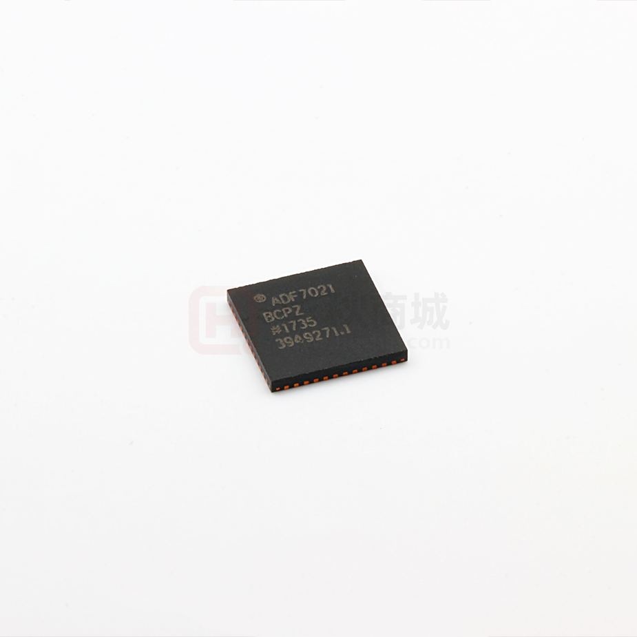
ORDERING GUIDE
Model1
ADF7021BCPZ
ADF7021BCPZ-RL
ADF7021BCPZ-RL7
EVAL-ADF70XXMBZ2
EVAL-ADF7021DBJZ
EVAL-ADF7021DBZ2
EVAL-ADF7021DBZ3
EVAL-ADF7021DBZ5
EVAL-ADF7021DBZ6
EVAL-ADF7021DB9Z
1
2
Temperature Range
−40°C to +85°C
−40°C to +85°C
−40°C to +85°C
Package Description2
48-Lead Lead Frame Chip Scale Package [LFCSP_WQ]
48-Lead Lead Frame Chip Scale Package [LFCSP_WQ]
48-Lead Lead Frame Chip Scale Package [LFCSP_WQ]
Mother Board
426 MHz to 429 MHz Daughter Board
860 MHz to 870 MHz Daughter Board
431 MHz to 470 MHz Daughter Board
80 MHz to 650 MHz Daughter Board
608 MHz to 614 MHz Daughter Board
169 MHz Daughter Board
Z = RoHS Compliant Part.
Maximum ordering quantity for all daughter boards is three. EVAL-ADF70XXMBZ2 is the required mother board for the daughter boards.
©2007–2016 Analog Devices, Inc. All rights reserved. Trademarks and
registered trademarks are the property of their respective owners.
D05876-0-9/16(D)
Rev. D | Page 62 of 62
Package Option
CP-48-5
CP-48-5
CP-48-5
�


 工商网监
湘ICP备2023018690号
工商网监
湘ICP备2023018690号
