Preliminary Technical Data
FEATURES
2Ω Max On Resistance 0.5Ω Max On Resistance Flatness 200mA Continuous current 33 V supply range Fully specified at +12 V, ±15 V, ±5 V No VL supply required 3 V logic-compatible inputs Rail-to-rail operation 14-lead TSSOP and 16-lead LFCSP
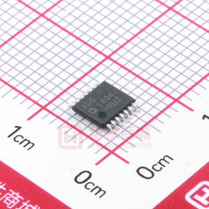
2Ω Max On Resistance, ±15 V/12 V/±5 V 4:1 iCMOS™ Multiplexer ADG1404
FUNCTIONAL BLOCK DIAGRAM
ADG1404
S1 S2 S3 S4 D
1 OF 4 DECODER
APPLICATIONS
Automatic test equipment Data aquisition systems Battery-powered systems Sample-and-hold systems Audio signal routing Communication systems Relay Replacement
A0
A1
EN
Figure 1.
GENERAL DESCRIPTION
The ADG1404 is a complementary metal-oxide semiconductor (CMOS) analog multiplexer, comprising four single channels designed on an iCMOS process. iCMOS (industrial CMOS) is a modular manufacturing process that combines high voltage CMOS and bipolar technologies. It enables the development of a wide range of high performance analog ICs capable of 33 V operation in a footprint that no previous generation of high voltage parts has been able to achieve. Unlike analog ICs using conventional CMOS processes, iCMOS components can tolerate high supply voltages while providing increased performance, dramatically lower power consumption, and reduced package size. The on resistance profile is very flat over the full analog input range ensuring excellent linearity and low distortion when switching audio signals. iCMOS construction ensures ultralow power dissipation, making the parts ideally suited for portable and batterypowered instruments. The ADG1404 switches one of four inputs to a common output, D, as determined by the 3-bit binary address lines, A0, A1, and EN. Logic 0 on the EN pin disables the device. Each switch conducts equally well in both directions when on and has an input signal range that extends to the supplies. In the off condition, signal levels up to the supplies are blocked. All switches exhibit break-before-make switching action. Inherent in the design is low charge injection for minimum transients when switching the digital inputs.
PRODUCT HIGHLIGHTS
1. 2. 3. 4. 5. 6. 2Ω Max On Resistance over temperature. Minimum distortion 3 V logic-compatible digital inputs: VIH = 2.0 V, VIL = 0.8 V No VL logic power supply required. Ultralow power dissipation:
很抱歉,暂时无法提供与“ADG1404”相匹配的价格&库存,您可以联系我们找货
免费人工找货