1 Ω Typical On Resistance, ±5 V, +12 V,
+5 V, and +3.3 V Dual SPDT Switches
ADG1636
Data Sheet
FEATURES
FUNCTIONAL BLOCK DIAGRAMS
1 Ω typical on resistance
0.2 Ω on resistance flatness
±3.3 V to ±8 V dual supply operation
3.3 V to 16 V single supply operation
No VL supply required
3 V logic-compatible inputs
Rail-to-rail operation
Continuous current per channel
LFCSP: 385 mA
TSSOP: 238 mA
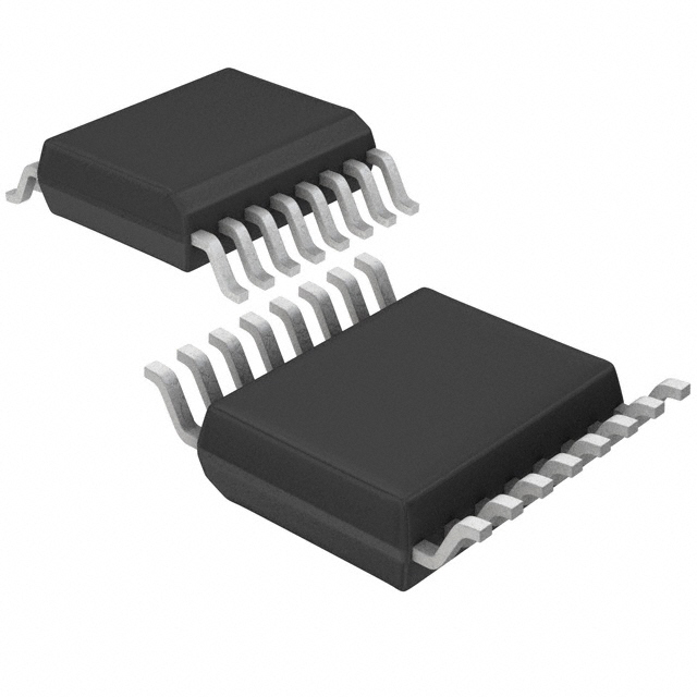
16-lead TSSOP and 16-lead, 4 mm × 4 mm LFCSP
ADG1636
S1A
D1
S1B
IN1
IN2
S2A
D2
NOTES
1. SWITCHES SHOWN FOR A LOGIC 1 INPUT.
APPLICATIONS
07983-001
S2B
Figure 1. 16-Lead TSSOP
Communication systems
Medical systems
Audio signal routing
Video signal routing
Automatic test equipment
Data acquisition systems
Battery-powered systems
Sample-and-hold systems
Relay replacements
ADG1636
S1A
S2A
D1
D2
S1B
S2B
IN1 IN2 EN
NOTES
1. SWITCHES SHOWN FOR A 1 INPUT LOGIC.
07983-002
LOGIC
Figure 2. 16-Lead LFCSP
GENERAL DESCRIPTION
The ADG1636 is a monolithic CMOS device containing two
independently selectable single-pole/double-throw (SPDT)
switches. An EN input is used to enable or disable the device.
When disabled, all channels are switched off. Each switch conducts
equally well in both directions when on and has an input signal
range that extends to the supplies. In the off condition, signal
levels up to the supplies are blocked. Both switches exhibit
break-before-make switching action for use in multiplexer
applications.
The CMOS construction ensures ultralow power dissipation,
making the devices ideally suited for portable and batterypowered instruments.
PRODUCT HIGHLIGHTS
1.
2.
3.
4.
5.
6.
1.6 Ω maximum on resistance over temperature.
Minimum distortion: THD + N = 0.007%.
3 V logic-compatible digital inputs: VINH = 2.0 V, VINL = 0.8 V.
No VL logic power supply required.
Ultralow power dissipation:
很抱歉,暂时无法提供与“ADG1636BRUZ”相匹配的价格&库存,您可以联系我们找货
免费人工找货