2.5 V/3.3 V, 2:1 Multiplexer/ Demultiplexer Bus Switch ADG3248
FEATURES 225 ps Propagation Delay through the Switch 4.5 Switch Connection between Ports Data Rate 1.244 Gbps 2.5 V/3.3 V Supply Operation Level Translation 3.3 V to 2.5 V 2.5 V to 1.8 V Small Signal Bandwidth 610 MHz 6-Lead SC70 Package APPLICATIONS 3.3 V to 2.5 V Voltage Translation 2.5 V to 1.8 V Voltage Translation Bus Switching Docking Stations Memory Switching Analog Switch Applications FUNCTIONAL BLOCK DIAGRAM
ADG3248
A0 B A1
IN
SWITCHES SHOWN FOR A LOGIC 0 INPUT
GENERAL DESCRIPTION
PRODUCT HIGHLIGHTS
The ADG3248 is a 2.5 V or 3.3 V, high performance 2:1 multiplexer/demultiplexer. It is designed on a low voltage CMOS process, which provides low power dissipation yet gives high switching speed and very low on resistance. This allows the input to be connected to the output without additional propagation delay or generating additional ground bounce noise. Each switch of the ADG3248 conducts equally well in both directions when on. The ADG3248 exhibits break-before-make switching action, preventing momentary shorting when switching channels. The ADG3248 is available in a tiny 6-lead SC70 package.
1. 2. 3. 4.
3.3 V or 2.5 V supply operation. Extremely low propagation delay through switch. 4.5 Ω switches connect inputs to outputs. Tiny SC70 package.
R EV. 0
Information furnished by Analog Devices is believed to be accurate and reliable. However, no responsibility is assumed by Analog Devices for its use, nor for any infringements of patents or other rights of third parties that may result from its use. No license is granted by implication or otherwise under any patent or patent rights of Analog Devices. Trademarks and registered trademarks are the property of their respective companies.
One Technology Way, P.O. Box 9106, Norwood, MA 02062-9106, U.S.A. Tel: 781/329-4700 www.analog.com Fax: 781/326-8703 © 2003 Analog Devices, Inc. All rights reserved.
�ADG3248–SPECIFICATIONS1
Parameter Symbol DC ELECTRICAL CHARACTERISTICS Input High Voltage VINH VINH Input Low Voltage VINL VINL Input Leakage Current II OFF State Leakage Current IOZ ON State Leakage Current Maximum Pass Voltage VP CAPACITANCE3 A Port Off Capacitance B Port Off Capacitance A, B Port On Capacitance Control Input Capacitance SWITCHING CHARACTERISTICS3 Propagation Delay A to B or B to A, tPD4 Propagation Delay Matching5 Transition Time Break-before-Make Time Maximum Data Rate Channel Jitter DIGITAL SWITCH On Resistance
(VCC = 2.3 V to 3.6 V, GND = 0 V, all specifications TMIN to TMAX, unless otherwise noted.)
B Version Typ2 Max
Conditions VCC = 2.7 V to 3.6 V VCC = 2.3 V to 2.7 V VCC = 2.7 V to 3.6 V VCC = 2.3 V to 2.7 V 0 ≤ A, B ≤ VCC 0 ≤ A, B ≤ VCC VA/VB = VCC = 3.3 V, IO = –5 µA VA/VB = VCC = 2.5 V, IO= –5 µA f = 1 MHz f = 1 MHz f = 1 MHz f = 1 MHz CL = 50 pF, VCC = 3 V RL = 510 Ω, CL = 50 pF RL = 510 Ω, CL = 50 pF VCC = 3.3 V; VA/VB = 2 V VCC = 3.3 V; VA/VB = 2 V VCC = 3 V, VA = 0 V, IBA = 8 mA VCC = 3 V, VA = 1.7 V, IBA = 8 mA VCC = 2.3 V, VA = 0 V, IBA = 8 mA VCC = 2.3 V, VA = 1 V, IBA = 8 mA VCC = 3 V, VA = 0 V, IA = 8 mA
Min 2.0 1.7
Unit V V V V µA µA µA V V pF pF pF pF
2.0 1.5
± 0.01 ± 0.01 ± 0.01 2.5 1.8 3.5 4.5 8.5 4
0.8 0.7 ±1 ±1 ±1 2.9 2.1
CA OFF CB OFF C A, C B O N CIN tPHL, tPLH tTRANS tBBM
5
16 10 1.244 45 4.5 12 5 9 0.1
0.225 5 29
ns ps ns ns Gbps ps p-p Ω Ω Ω Ω Ω V µA
RON
On Resistance Matching POWER REQUIREMENTS VCC Quiescent Power Supply Current
RON
8 28 9 18 0.5 3.6 1
2.3 ICC Digital Inputs = 0 V or VCC 0.01
NOTES 1 Temperature range is as follows: B Version: –40 °C to +85°C. 2 Typical values are at 25 °C, unless otherwise stated. 3 Guaranteed by design, not subject to production test. 4 The digital switch contributes no propagation delay other than the RC delay of the typical R ON of the switch and the load capacitance when driven by an ideal voltage source. Since the time constant is much smaller than the rise/fall times of typical driving signals, it adds very little propagation delay to the system. Propagation delay of the digital switch when used in a system is determined by the driving circuit on the driving side of the switch and its interaction with the load on the driven side. 5 Propagation delay matching between channels is calculated from the on resistance matching and load capacitance of 50 pF. Specifications subject to change without notice.
–2–
R EV. 0
�ADG3248
ABSOLUTE MAXIMUM RATINGS *
(TA = 25°C, unless otherwise noted.)
PIN CONFIGURATION 6-Lead SC70
A0 1
6
VCC to GND . . . . . . . . . . . . . . . . . . . . . . . . . –0.5 V to +4.6 V Digital Inputs to GND . . . . . . . . . . . . . . . . . –0.5 V to +4.6 V DC Input Voltage . . . . . . . . . . . . . . . . . . . . . –0.5 V to +4.6 V DC Output Current . . . . . . . . . . . . . . . . . 25 mA per Channel Operating Temperature Range Industrial (B Version) . . . . . . . . . . . . . . . . . –40°C to +85°C Storage Temperature Range . . . . . . . . . . . . –65°C to +150°C Junction Temperature . . . . . . . . . . . . . . . . . . . . . . . . . . 150°C JA Thermal Impedance . . . . . . . . . . . . . . . . . . . . . . 332°C/W Lead Temperature, Soldering (10 sec) . . . . . . . . . . . . . 300°C IR Reflow, Peak Temperature (
很抱歉,暂时无法提供与“ADG3248BKS-R2”相匹配的价格&库存,您可以联系我们找货
免费人工找货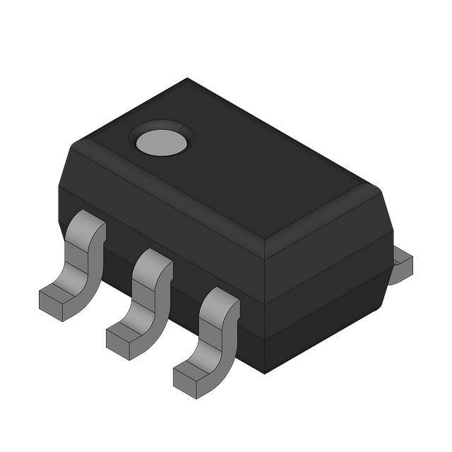


 工商网监
湘ICP备2023018690号
工商网监
湘ICP备2023018690号
