Precision MEMS IMU Module
ADIS16465
Data Sheet
FEATURES
GENERAL DESCRIPTION
Triaxial, digital gyroscope
±125°/sec, ±500°/sec, ±2000°/sec dynamic range models
2°/hr in-run bias stability (ADIS16465-1)
0.15°/√hr angular random walk (ADIS16465-1 and
ADIS16465-2)
±0.05° axis to axis misalignment error
Triaxial, digital accelerometer, ±8 g
3.6 μg in-run bias stability
Triaxial, delta angle, and delta velocity outputs
Factory calibrated sensitivity, bias, and axial alignment
Calibration temperature range: −40°C to +85°C
SPI-compatible data communications
Programmable operation and control
Automatic and manual bias correction controls
Data ready indicator for synchronous data acquisition
External sync modes: direct, pulse, scaled, and output
On demand self test of inertial sensors
On demand self test of flash memory
Single-supply operation (VDD): 3.0 V to 3.6 V
2000 g mechanical shock survivability
Operating temperature range: −40°C to +105°C
The ADIS16465 is a precision, microelectric mechanical system
(MEMS), inertial measurement unit (IMU) that includes a triaxial
gyroscope and a triaxial accelerometer. Each inertial sensor in
the ADIS16465 combines with signal conditioning to optimize
dynamic performance. The factory calibration characterizes
each sensor for sensitivity, bias, alignment, linear acceleration
(gyroscope bias), and point of percussion (accelerometer location).
Therefore, each sensor has dynamic compensation formulas
that provide accurate sensor measurements over a broad set
of conditions.
The ADIS16465 provides a simple, cost effective method for
integrating accurate, multiaxis inertial sensing into industrial
systems, especially when compared to the complexity and
investment associated with discrete designs. All necessary motion
testing and calibration are part of the production process at the
factory, greatly reducing system integration time. Tight orthogonal
alignment simplifies inertial frame alignment in navigation
systems. The serial peripheral interface (SPI) and register
structure provide a simple interface for data collection and
configuration control.
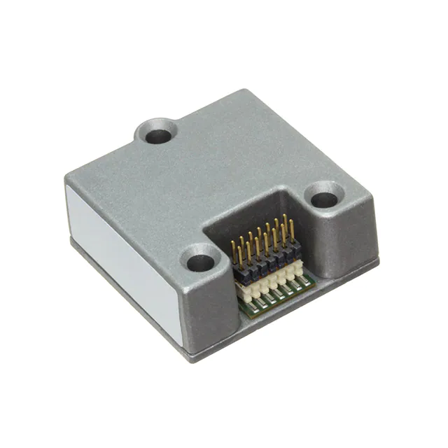
The ADIS16465 is in an aluminum module package that is
approximately 22.4 mm × 22.4 mm × 9 mm with a 14-lead
connector interface.
APPLICATIONS
Navigation, stabilization, and instrumentation
Unmanned and autonomous vehicles
Smart agriculture and construction machinery
Factory/industrial automation, robotics
Virtual/augmented reality
Internet of Moving Things
FUNCTIONAL BLOCK DIAGRAM
DR
SELF TEST
RST
POWER
MANAGEMENT
INPUT/OUTPUT
OUTPUT
DATA
REGISTERS
TRIAXIAL
GYROSCOPE
TRIAXIAL
ACCELEROMETER
CONTROLLER
CALIBRATION
AND
FILTERS
GND
CS
SPI
USER
CONTROL
REGISTERS
SCLK
DIN
DOUT
CLOCK
ADIS16465
SYNC
15438-001
TEMPERATURE
SENSOR
VDD
Figure 1.
Rev. C
Document Feedback
Information furnished by Analog Devices is believed to be accurate and reliable. However, no
responsibility is assumed by Analog Devices for its use, nor for any infringements of patents or other
rights of third parties that may result from its use. Specifications subject to change without notice.
No license is granted by implication or otherwise under any patent or patent rights of Analog
Devices. Trademarks and registered trademarks are the property of their respective owners.
One Technology Way, P.O. Box 9106, Norwood, MA 02062-9106, U.S.A.
Tel: 781.329.4700 ©2017–2020 Analog Devices, Inc. All rights reserved.
Technical Support
www.analog.com
�ADIS16465
Data Sheet
TABLE OF CONTENTS
Features .............................................................................................. 1
Device Configuration ................................................................ 15
Applications ...................................................................................... 1
User Register Memory Map.......................................................... 16
General Description ......................................................................... 1
User Register Defintions ............................................................... 18
Functional Block Diagram .............................................................. 1
Gyroscope Data .......................................................................... 18
Revision History ............................................................................... 2
Delta Angles ................................................................................ 21
Specifications .................................................................................... 3
Delta Velocity ............................................................................. 22
Timing Specifications .................................................................. 5
Calibration .................................................................................. 24
Absolute Maximum Ratings ....................................................... 7
Applications Information ............................................................. 30
Thermal Resistance ...................................................................... 7
Assembly and Handling Tips ................................................... 30
ESD Caution.................................................................................. 7
Power Supply Considerations .................................................. 30
Pin Configuration and Function Descriptions ............................ 8
Breakout Board ........................................................................... 30
Typical Performance Characteristics ............................................. 9
Serial Port Operation ................................................................. 31
Theory of Operation ...................................................................... 11
Digital Resolution of Gyroscopes and Accelerometers ........ 31
Introduction ................................................................................ 11
PC-Based Evaluation Tools ...................................................... 32
Inertial Sensor Signal Chain ..................................................... 11
Ordering Information.................................................................... 33
Register Structure ....................................................................... 12
Outline Dimensions ................................................................... 33
Serial Peripheral Interface (SPI) ............................................... 13
Ordering Guide .......................................................................... 33
Data Ready (DR) ........................................................................ 13
Reading Sensor Data .................................................................. 14
REVISION HISTORY
4/2020—Rev. B to Rev. C
Changes to Table 1 ........................................................................... 3
Changes to Figure 18 ..................................................................... 10
Changes to Reading Sensor Data Section and Burst Read
Function Section ............................................................................. 14
3/2019—Rev. A to Rev. B
Changes to Serial Peripheral Interface (SPI) Section ................ 13
Changes to Figure 32 ..................................................................... 14
Changes to Table 10 ....................................................................... 18
Added Serial Port Operation Section, Maximum Throughput
Section, and Serial Port SCLK Underrun/Overrun Conditions .. 32
Moved Gyroscope Data Width (Digital Resolution) Section... 32
Moved Accelerometer Data Width (Digital Resolution) Section . 32
Added Digital Resolution of Gyroscopes and Accelerometers
Section .............................................................................................. 32
11/2018—Rev. 0 to Rev. A
Changes to Table 1 ........................................................................... 3
Changes to Table 2 ........................................................................... 5
Changes to Figure 5.......................................................................... 6
Added Figure 11, Figure 12, and Figure 13; Renumbered
Sequentially ........................................................................................9
Added Figure 14, Figure 15, Figure 16, and Figure 17 .............. 10
Changes to Figure 18, Figure 19, and Figure 20 ........................ 11
Changes to Figure 22 and Figure 23 ............................................ 12
Added Gyroscope Data Width (Digital Resolution) Section ... 18
Changes to Gyroscope Measurement Range/Scale Factor Section,
Table 11, Gyroscope Data Formatting Section, Table 12, Table 13,
Table 17, Table 21, and Table 25 .................................................. 19
Added Accelerometer Data Width (Digital Resolution) Section
........................................................................................................... 20
Changed Accelerometer Resolution Section to Accelerometer
Data Formatting Section ............................................................... 20
Change to Calibration, Accelerometer Bias (XA_BIAS_LOW
and XA_BIAS_HIGH) Section..................................................... 25
Change to Filter Control Register (FILT_CTRL) Section ........ 26
Changes to Direct Sync Mode Section ........................................ 27
Changes to Pulse Sync Mode Section .......................................... 28
Changes to Sensor Self Test Section ............................................ 29
Changes to Outline Dimensions .................................................. 33
12/2017—Revision 0: Initial Version
Rev. C | Page 2 of 33
�Data Sheet
ADIS16465
SPECIFICATIONS
Case temperature (TC) = 25°C, VDD = 3.3 V, angular rate = 0°/sec, and dynamic range = ±2000°/sec ± 1 g, unless otherwise noted.
Table 1.
Parameter
GYROSCOPES
Dynamic Range
Sensitivity
Repeatability1
Error over Temperature
Misalignment Error
Nonlinearity2
Bias
Repeatability1
In-Run Bias Stability
Angular Random Walk
Error over Temperature
Linear Acceleration Effect
Vibration Rectification Effect
Output Noise
Rate Noise Density
3 dB Bandwidth
Sensor Resonant Frequency
ACCELEROMETERS3
Dynamic Range
Sensitivity
Repeatability1
Error over Temperature
Misalignment Error
Nonlinearity
Test Conditions/Comments
Min
ADIS16465-1
ADIS16465-2
ADIS16465-3
ADIS16465-1, 16-bit
ADIS16465-2, 16-bit
ADIS16465-3, 16-bit
ADIS16465-1, 32-bit
ADIS16465-2, 32-bit
ADIS16465-3, 32-bit
−40°C ≤ TC ≤ +85°C, 1 σ
−40°C ≤ TC ≤ +85°C, 1 σ
Axis to axis, 1 σ
ADIS16465-1, full scale (FS) = 125°/sec
ADIS16465-2, FS = 500°/sec
ADIS16465-3, FS = 2000°/sec
±125
±500
±2000
−40°C ≤ TC ≤ +85°C, 1 σ
ADIS16465-1, 1 σ
ADIS16465-2, 1 σ
ADIS16465-3, 1 σ
ADIS16465-1, 1 σ
ADIS16465-2, 1 σ
ADIS16465-3, 1 σ
−40°C ≤ TC ≤ +85°C, 1 σ
Any direction, 1 σ
Random vibration, 2 g rms, bandwidth = 50 Hz to 2 kHz
ADIS16465-1, 1 σ, no filtering, x-axis
ADIS16465-1, 1 σ, no filtering, y-axis and z-axis
ADIS16465-2, 1 σ, no filtering, x-axis
ADIS16465-2, 1 σ, no filtering, y-axis and z-axis
ADIS16465-3, 1 σ, no filtering, x-axis
ADIS16465-3, 1 σ, no filtering, y-axis and z-axis
ADIS16465-1, 10 Hz to 40 Hz, x-axis
ADIS16465-1, 10 Hz to 40 Hz, y-axis and z-axis
ADIS16465-2, 10 Hz to 40 Hz, x-axis
ADIS16465-2, 10 Hz to 40 Hz, y-axis and z-axis
ADIS16465-3, 10 Hz to 40 Hz, x-axis
ADIS16465-3, 10 Hz to 40 Hz, y-axis and z-axis
Typ
Max
Unit
160
40
10
10,485,760
2,621,440
655,360
±0.3
±0.3
±0.05
0.2
0.2
0.25
°/sec
°/sec
°/sec
LSB/°/sec
LSB/°/sec
LSB/°/sec
LSB/°/sec
LSB/°/sec
LSB/°/sec
%
%
Degrees
% FS
% FS
% FS
0.4
2
2.5
6
0.15
0.15
0.26
±0.2
0.009
0.0005
0.05
0.07
0.05
0.08
0.11
0.16
0.002
0.003
0.002
0.003
0.004
0.0065
550
66
°/sec
°/hr
°/hr
°/hr
°/√hr
°/√hr
°/√hr
°/sec
°/sec/g
°/sec/g2
°/sec rms
°/sec rms
°/sec rms
°/sec rms
°/sec rms
°/sec rms
°/sec/√Hz rms
°/sec/√Hz rms
°/sec/√Hz rms
°/sec/√Hz rms
°/sec/√Hz rms
°/sec/√Hz rms
Hz
kHz
262,144,000
±0.2
±0.1
±0.05
0.25
0.5
1.5
g
LSB/g
%
%
Degrees
% FS
% FS
% FS
Each axis
±8
32-bit data format
−40°C ≤ TC ≤ +85°C, 1 σ
−40°C ≤ TC ≤ +85°C, 1 σ
Axis to axis
Best fit straight line, ±2 g
Best fit straight line, ±8 g, x-axis
Best fit straight line, ±8 g, y-axis and z-axis
Rev. C | Page 3 of 33
�ADIS16465
Parameter
Bias
Repeatability1
In-Run Bias Stability
Velocity Random Walk
Error over Temperature
Output Noise
Noise Density
3 dB Bandwidth
Sensor Resonant Frequency
TEMPERATURE SENSOR
Scale Factor
LOGIC INPUTS4
Input Voltage
High, VIH
Low, VIL
RST Pulse Width
Input Current
Logic 1, IIH
Logic 0, IIL
All Pins Except RST
RST Pin
Input Capacitance, CIN
DIGITAL OUTPUTS
Output Voltage
High, VOH
Low, VOL
FLASH MEMORY
Data Retention6
FUNCTIONAL TIMES7
Power-On Start-Up Time
Reset Recovery Time
Factory Calibration Restore
Flash Memory Backup
Flash Memory Test Time
Self Test Time9
CONVERSION RATE
Initial Clock Accuracy
Sync Input Clock
POWER SUPPLY, VDD
Power Supply Current10
Data Sheet
Test Conditions/Comments
Min
−40°C ≤ TC ≤ +85°C, 1 σ
1σ
1σ
−40°C ≤ TC ≤ +85°C, 1 σ
No filtering
Bandwidth = 10 Hz to 40 Hz (no filtering)
Typ
Max
Unit
Y-axis and z-axis
X-axis
1.4
3.6
0.012
±1
0.6
23
600
2.4
2.2
mg
μg
m/sec/√hr
mg
mg rms
μg/√Hz rms
Hz
kHz
kHz
Output = 0x0000 at 0°C (±5°C)
0.1
°C/LSB
2.0
0.8
V
V
μs
10
μA
10
μA
mA
pF
1
VIH = 3.3 V
VIL = 0 V
0.33
10
ISOURCE = 0.5 mA
ISINK = 2.0 mA
Endurance5
TJ = 85°C
Time until data is available
2.4
0.4
10000
20
259
198
198
142
72
32
14
2000
3
Register GLOB_CMD, Bit 7 = 1 (see Table 113)
RST pulled low, then restored to high8
Register GLOB_CMD, Bit 1 = 1 (see Table 113)
Register GLOB_CMD, Bit 3 = 1 (see Table 113)
Register GLOB_CMD, Bit 4 = 1 (see Table 113)
Register GLOB_CMD, Bit 2 = 1 (see Table 113)
Operating voltage range
Normal mode, VDD = 3.3 V
1
1.9
3.0
44
2.1
3.6
55
V
V
Cycles
Years
ms
ms
ms
ms
ms
ms
ms
SPS
%
kHz
V
mA
Bias repeatability provides an estimate for long-term drift in the bias, as observed during 500 hours of High-Temperature Operating Life (HTOL) at +105°C.
This measurement is based on the deviation from a best fit linear model.
3
All specifications associated with the accelerometers relate to the full-scale range of ±8 g, unless otherwise noted.
4
The digital input/output signals use a 3.3 V system.
5
Endurance is qualified as per JEDEC Standard 22, Method A117, measured at −40°C, +25°C, +85°C, and +125°C.
6
The data retention specification assumes a junction temperature (TJ) of 85°C per JEDEC Standard 22, Method A117. Data retention lifetime decreases with TJ.
7
These times do not include thermal settling and internal filter response times, which may affect overall accuracy.
8
The RST line must be in a low state for at least 10 μs to ensure a proper reset initiation and recovery.
9
The self test time can extend when using external clock rates lower than 2000 Hz.
10
Power supply current transients can reach 100 mA during initial startup or reset recovery.
2
Rev. C | Page 4 of 33
�Data Sheet
ADIS16465
TIMING SPECIFICATIONS
TA = 25°C, VDD = 3.3 V, unless otherwise noted.
Table 2.
Normal Mode
Min Typ Max
0.1
2
16
24
200
Parameter
fSCLK
tSTALL
tREADRATE
tCS
Description
Serial clock
Stall period between data
Read rate
Chip select to SCLK edge
tDAV
tDSU
tDHD
tSCLKR, tSCLKF
tDR, tDF
tSFS
t1
DOUT valid after SCLK edge
DIN setup time before SCLK rising edge
DIN hold time after SCLK rising edge
SCLK rise/fall times
DOUT rise/fall times
CS high after SCLK edge
Input sync positive pulse width; pulse sync mode,
Register MSC_CTRL, Bits[4:1] = 101 (binary, see Table 105)
Input sync to data ready valid transition
Direct sync mode, Register MSC_CTRL, Bits[4:2] = 001 (binary, see Table 105)
Pulse sync mode, Register MSC_CTRL, Bits[4:2] = 101 (binary, see Table 105)
Data invalid time
Input sync period2
tSTDR
tNV
t2
1
2
Burst Read Mode
Min1 Typ Max
0.1
1
N/A
200
25
25
25
50
25
50
5
5
12.5
12.5
0
5
5
5
12.5
12.5
0
5
256
256
20
256
256
20
477
477
Timing Diagrams
tSCLKR
tSCLKF
tCS
tSFS
SCLK
2
3
4
5
tDAV
MSB
DOUT
DB14
R/W
A6
15
16
tDR
DB13
tDSU
DIN
6
DB12
DB11
tDHD
A5
DB10
DB2
DB1
LSB
tDF
A4
A3
A2
D2
D1
15438-002
1
LSB
Figure 2. SPI Timing and Sequence Diagram
tREADRATE
tSTALL
15438-003
CS
SCLK
Figure 3. Stall Time and Data Rate Timing Diagram
Rev. C | Page 5 of 33
ns
ns
ns
ns
ns
ns
μs
μs
μs
μs
μs
N/A means not applicable.
This specification is rounded up from the cycle time that comes from the maximum input clock frequency (2100 Hz).
CS
Unit
MHz
μs
μs
ns
�ADIS16465
Data Sheet
t2
tSTDR
t1
DR
tNV
15438-004
SYNC
Figure 4. Input Clock Timing Diagram, Pulse Sync Mode, Register MSC_CTRL, Bits[4:2] = 101 (Binary)
t2
t1
SYNC
tNV
tSTDR
15438-005
DR
Figure 5. Input Clock Timing Diagram, Direct Sync Mode, Register MSC_CTRL, Bits[4:2] = 001 (Binary)
Rev. C | Page 6 of 33
�Data Sheet
ADIS16465
ABSOLUTE MAXIMUM RATINGS
THERMAL RESISTANCE
Table 3.
Thermal performance is directly linked to printed circuit board
(PCB) design and operating environment. Careful attention to
PCB thermal design is required.
Parameter
Mechanical Shock Survivability
Any Axis, Unpowered
Any Axis, Powered
VDD to GND
Digital Input Voltage to GND
Digital Output Voltage to GND
Calibration Temperature Range
Operating Temperature Range
Storage Temperature Range1
Barometric Pressure
1
Rating
The ADIS16465 is a multichip module that includes many active
components. The values in Table 4 identify the thermal
response of the hottest component inside of the ADIS16465,
with respect to the overall power dissipation of the module.
This approach enables a simple method for predicting the
temperature of the hottest junction, based on either ambient or
case temperature.
2000 g
2000 g
−0.3 V to +3.6 V
−0.3 V to VDD + 0.2 V
−0.3 V to VDD + 0.2 V
−40°C to +85°C
−40°C to +105°C
−65°C to +150°C
2 bar
For example, when the ambient temperature is 70°C, the hottest
junction temperature (TJ) inside of the ADIS16465 is 75.3°C.
Extended exposure to temperatures that are lower than −40°C or higher
than +105°C can adversely affect the accuracy of the factory calibration.
TJ = θJA × VDD × IDD + 70°C
Stresses at or above those listed under Absolute Maximum
Ratings may cause permanent damage to the product. This is a
stress rating only; functional operation of the product at these
or any other conditions above those indicated in the operational
section of this specification is not implied. Operation beyond
the maximum operating conditions for extended periods may
affect product reliability.
TJ = 36.5°C/W × 3.3 V × 0.044 A + 70°C
TJ = 75.3°C
Table 4. Thermal Resistance
Package Type
ML-14-63
1
θJA1
36.5°C/W
θJC2
16.9C/W
Mass (g)
15
θJA is the natural convection junction to ambient thermal resistance
measured in a one cubic foot sealed enclosure.
θJC is the junction to case thermal resistance.
3
Thermal impedance values come from direct observation of the hottest
temperature inside of the ADIS16465 when it is attached to an FR4-08 PCB
that has two metal layers and has a thickness of 0.063 inches.
2
ESD CAUTION
Rev. C | Page 7 of 33
�ADIS16465
Data Sheet
PIN CONFIGURATION AND FUNCTION DESCRIPTIONS
ADIS16465
PIN 1
TOP VIEW
(Not to Scale)
DNC
DIN
SCLK
DR
9
7
5
3
1
14
12
10
8
6
4
2
DNC
DNC
RST
CS
DOUT
SYNC
NOTES
1. THIS REPRESENTS THE PIN ASSIGNMENTS WHEN
LOOKING DOWN AT THE CONNECTOR. SEE FIGURE 7.
2. MATING CONNECTOR:
SAMTEC CLM-107-02 SERIES OR EQUIVALENT.
3. DNC = DO NOT CONNECT.
15438-007
DNC
11
15438-006
GND
VDD
13
DNC
PIN 14
Figure 6. Pin Assignments, Bottom View
Figure 7. Pin Assignments, Package Level View
Table 5. Pin Function Descriptions
Pin No.
1
2
3
4
5
6
7
8
9
10
11
12
13
14
Mnemonic
DR
SYNC
SCLK
DOUT
DIN
CS
DNC
RST
DNC
DNC
VDD
DNC
GND
DNC
Type
Output
Input/output
Input
Output
Input
Input
Not applicable
Input
Not applicable
Not applicable
Supply
Not applicable
Supply
Not applicable
Description
Data Ready Indicator.
External Sync Input/Output, per MSC_CTRL. See Table 105.
SPI Serial Clock.
SPI Data Output. This pin clocks the output on the SCLK falling edge.
SPI Data Input. This pin clocks the input on the SCLK rising edge.
SPI Chip Select.
Do Not Connect. Do not connect to this pin.
Reset.
Do Not Connect. Do not connect to this pin.
Do Not Connect. Do not connect to this pin.
Power Supply.
Do Not Connect. Do not connect to this pin.
Power Ground.
Do Not Connect. Do not connect to this pin.
Rev. C | Page 8 of 33
�Data Sheet
ADIS16465
TYPICAL PERFORMANCE CHARACTERISTICS
1000
ALLAN DEVIATION (µg)
100
10
1
0.1
0.001
0.01
0.1
1
10
100
1000
10000 100000
INTEGRATION PERIOD (Seconds)
100
10
1
0.1
0.001
0.1
1
10
100
1000
10000 100000
Figure 11. Accelerometer Allan Deviation, TC = 25°C
0.4
X-AXIS
Y-AXIS
Z-AXIS
0.3
100
SENSITIVITY ERROR (%)
ALLAN DEVIATION (Degrees/Hour)
0.01
INTEGRATION PERIOD (Seconds)
Figure 8. Gyroscope Allan Deviation, TC = 25°C, ADIS16465-1
1000
X-AXIS
Y-AXIS
Z-AXIS
15438-111
X-AXIS
Y-AXIS
Z-AXIS
15438-008
ALLAN DEVIATION (Degrees/Hour)
1000
10
1
0.2
0.1
µ + 1σ
0
–0.1
µ – 1σ
–0.2
µ
0.01
0.1
1
10
100
1000
10000 100000
INTEGRATION PERIOD (Seconds)
Figure 9. Gyroscope Allan Deviation, TC = 25°C, ADIS16465-2
–40
–20
0
20
40
60
80
100
AMBIENT TEMPERATURE (°C)
Figure 12. ADIS16465-1 Gyroscope Sensitivity Error vs. Ambient Temperature
0.4
X-AXIS
Y-AXIS
Z-AXIS
0.3
SENSITIVITY ERROR (%)
100
10
1
0.2
0.1
µ + 1σ
0
–0.1
µ
–0.2
µ – 1σ
0.1
0.001
0.01
0.1
1
10
100
1000
10000 100000
INTEGRATION PERIOD (Seconds)
Figure 10. Gyroscope Allan Deviation, TC = 25°C, ADIS16465-3
–0.4
–60
–40
–20
0
20
40
60
AMBIENT TEMPERATURE (°C)
80
100
15438-113
–0.3
15438-010
ALLAN DEVIATION (Degrees/Hour)
1000
–0.4
–60
15438-009
0.1
0.001
15438-112
–0.3
Figure 13. ADIS16465-2 Gyroscope Sensitivity Error vs. Ambient Temperature
Rev. C | Page 9 of 33
�ADIS16465
Data Sheet
0.4
0.5
0.4
BIAS ERROR (Degrees/Second)
0.2
0.1
0
µ + 1σ
–0.1
–0.2
µ – 1σ
µ
–0.3
0.2
µ + 1σ
0.1
0
–0.1
µ
µ – 1σ
–0.2
–0.3
–0.4
–40
–20
0
20
40
60
80
100
AMBIENT TEMPERATURE (°C)
–0.5
–60
15438-114
–0.4
–60
0.3
Figure 14. ADIS16465-3 Gyroscope Sensitivity Error vs. Ambient Temperature
–40
–20
0
20
40
60
80
100
AMBIENT TEMPERATURE (°C)
15438-117
SENSITIVITY ERROR (%)
0.3
Figure 17. ADIS16465-3 Gyroscope Bias Error vs. Ambient Temperature
0.5
0.3
0.2
BIAS ERROR (Degrees/Second)
BIAS ERROR (Degrees/Second)
0.4
µ + 1σ
0.1
0
–0.1
µ
µ – 1σ
–0.2
–0.3
–40
–20
0
20
40
60
80
100
AMBIENT TEMPERATURE (°C)
Figure 15. ADIS16465-1 Gyroscope Bias Error vs. Ambient Temperature
0
BIAS ERROR (Degrees/Second)
0.3
µ + 1σ
0.1
0
–0.1
µ
µ – 1σ
–0.3
–40
–20
0
20
40
60
AMBIENT TEMPERATURE (°C)
80
100
15438-116
–0.4
–0.5
–60
15
20
25
30
35
Figure 18. ADIS16465-3 Gyroscope Bias Error vs. Power-On Time at 25°C.
(Applicable to All ADIS16465 Models)
0.4
–0.2
10
POWER-ON TIME (Minutes)
0.5
0.2
5
15438-118
–0.5
–60
15438-115
–0.4
Figure 16. ADIS16465-2 Gyroscope Bias Error vs. Ambient Temperature
Rev. C | Page 10 of 33
�Data Sheet
ADIS16465
THEORY OF OPERATION
When using the factory default configuration for all user
configurable control registers, the ADIS16465 initializes and
automatically starts a continuous process of sampling, processing,
and loading calibrated sensor data into the output registers at a
rate of 2000 SPS.
The ADIS16465 provides three different modes of operation that
support the device using an external clock to control the internal
processing rate (fSM in Figure 20 and Figure 21) through the
SYNC pin. The MSC_CTRL register (see Table 105) provides the
configuration options for these external clock modes in Bits[4:2].
INERTIAL SENSOR SIGNAL CHAIN
Inertial Sensor Calibration
Figure 19 shows the basic signal chain for the inertial sensors in the
ADIS16465. This signal chain produces an update rate of 2000 SPS
in the output data registers when it operates in internal clock mode
(default, see Register MSC_CTRL, Bits[4:2] in Table 105).
The inertial sensor calibration function for the gyroscopes and the
accelerometers has two components: factory calibration and
user calibration (see Figure 22).
MEMS
SENSORS
BARTLETT
WINDOW
FIR
FILTER
AVERAGING
DECIMATING
FILTER
CALIBRATION
OUTPUT
DATA
REGISTERS
Figure 19. Signal Processing Diagram, Inertial Sensors
FROM
BARTLETT
WINDOW
FIR FILTER
fSG = 4100Hz
TO
BARTLETT
WINDOW
FIR FILTER
fSM = 2000Hz
15438-012
INTERNAL
DATA
REGISTER
Figure 20. Gyroscope Data Sampling
Accelerometer Data Sampling
The three accelerometers produce linear acceleration measurements
along the same orthogonal axes (x, y, and z) as the gyroscopes.
Figure 21 shows the data sampling plan for each accelerometer
when the ADIS16465 operates in internal clock mode (default,
see Register MSC_CTRL, Bits[4:2] in Table 105).
ADC
1 2
a(n)
2 nΣ
=1
÷2
2 × fSM = 4000Hz
Figure 21. Accelerometer Data Sampling
TO
BARTLETT
WINDOW
FIR FILTER
15438-013
MEMS
ACCELEROMETER
TO
AVERAGING
DECIMATING
FILTER
Figure 22. Inertial Sensor Calibration Processing
The three gyroscopes produce angular rate measurements around
three orthogonal axes (x, y, and z). Figure 20 shows the data
sampling plan for each gyroscope when the ADIS16465 operates
in internal clock mode (default, see Register MSC_CTRL, Bits[4:2]
in Table 105). Each gyroscope has an analog-to-digital converter
(ADC) and sample clock (fSG) that drives data sampling at a rate of
4100 Hz (±5%). The internal processor reads and processes this
data from each gyroscope at a rate of 2000 Hz (fSM).
ADC
USER
CALIBRATION
The factory calibration of the gyroscope applies the following
correction formulas to the data of each gyroscope:
Gyroscope Data Sampling
MEMS
GYROSCOPE
FACTORY
CALIBRATION
15438-014
External Clock Options
15438-011
INTRODUCTION
ω XC m11 m12
ωYC m21 m22
ωZC m31 m32
l11 l12
l21 l22
l31 l32
m13 ω X bX
m23 ωY bY
m33 ωZ bZ
l13 a XC
l23 aYC
l33 aZC
where:
ωXC, ωYC, and ωZC are the gyroscope outputs (post calibration).
m11, m12, m13, m21, m22, m23, m31, m32, and m33 provide scale and
alignment correction.
ωX, ωY, and ωZ are the gyroscope outputs (precalibration).
bX, bY, and bZ provide bias correction.
l11, l12, l13, l21, l22, l23, l31, l32, and l33 provide linear g correction
aXC, aYC, and aZC are the accelerometer outputs (post calibration).
All of the correction factors in this relationship come from
direct observation of the response of each gyroscope at multiple
temperatures over the calibration temperature range (−40°C ≤
TC ≤ +85°C). These correction factors are stored in the flash
memory bank, but they are not available for observation or
configuration. Register MSC_CTRL, Bit 7 (see Table 105)
provides the only user configuration option for the factory
calibration of the gyroscopes: an on/off control for the linear g
compensation. See Figure 45 for more details on the user
calibration options available for the gyroscopes.
Rev. C | Page 11 of 33
�ADIS16465
Data Sheet
0
p32
FROM
MEMS
SENSOR
p13 ω 2XC
p 23 ω 2YC
0 ω 2ZC
1 N
ω(n)
N nΣ
=1
1 N
ω(n)
N nΣ
=1
TO
FACTORY
CALIBRATION
Figure 23. Bartlett Window FIR Filter Signal Path
Averaging/Decimating Filter
where:
aXC, aYC, and aZC are the accelerometer outputs (post calibration).
m11, m12, m13, m21, m22, m23, m31, m32, and m33 provide scale and
alignment correction.
aX, aY, and aZ are the accelerometer outputs (precalibration).
bX, bY, and bZ provide bias correction.
p12, p13, p21, p23, p31, and p32 provide a point of percussion
alignment correction (see Figure 48).
ω2XC, ω2YC, and ω2ZC are the square of the gyroscope outputs
(post calibration).
All of the correction factors in this relationship come from direct
observation of the response of each accelerometer at multiple
temperatures over the calibration temperature range (−40°C ≤
TC ≤ +85°C). These correction factors are stored in the flash
memory bank, but they are not available for observation or
configuration. Register MSC_CTRL, Bit 6 (see Table 105) provides
the only user configuration option for the factory calibration of
the accelerometers: an on/off control for the point of percussion,
alignment function. See Figure 46 for more details on the user
calibration options available for the accelerometers.
The second digital filter averages multiple samples together to
produce each register update. In this type of filter structure, the
number of samples in the average is equal to the reduction in the
update rate for the output data registers. The DEC_RATE register
(see Table 109) provides the configuration controls for this filter.
FROM
USER
CALIBRATION
1 N
ω(n)
N nΣ
=1
÷N
TO OUTPUT
REGISTERS
Figure 24. Averaging/Decimating Filter Diagram
REGISTER STRUCTURE
All communication between the ADIS16465 and an external
processor involves either reading the contents of an output
register or writing configuration or command information to
a control register. The output data registers include the latest
sensor data, error flags, and identification information. The control
registers include sample rate, filtering, calibration, and diagnostic
options. Each user accessible register has two bytes (upper and
lower), each of which has a unique address. See Table 8 for a
detailed list of all user registers and the corresponding addresses.
TRIAXIAL
GYROSCOPE
TRIAXIAL
ACCELEROMETER
TEMPERATURE
SENSOR
SENSOR
SIGNAL
PROCESSING
OUTPUT
REGISTERS
CONTROLLER
CONTROL
REGISTERS
Figure 25. Basic Operation of the ADIS16465
Rev. C | Page 12 of 33
15438-017
p12
15438-016
0
p 21
p31
m13 a X b X
m23 aY bY
m33 a Z bZ
The Bartlett window finite impulse response (FIR) filter (see
Figure 23) contains two averaging filter stages in a cascade
configuration. The FILT_CTRL register (see Table 101) provides
the configuration controls for this filter.
SPI
a XC m11 m12
aYC m21 m22
a ZC m31 m32
Bartlett Window FIR Filter
15438-015
The factory calibration of the accelerometer applies the following
correction formulas to the data of each accelerometer:
�Data Sheet
ADIS16465
DATA READY (DR)
The SPI provides access to the user registers (see Table 8).
Figure 26 shows the most common connections between the
ADIS16465 and a SPI master device, which is often an embedded
processor that has an SPI-compatible interface. In this example,
the SPI master uses an interrupt service routine to collect data
every time the data ready (DR) signal pulses.
The factory default configuration provides users with a DR signal
on the DR pin (see Table 5) that pulses when the output data
registers update. Connect the DR pin to a pin on the embedded
processor to trigger data collection, on the second edge of this
pulse. Register MSC_CTRL, Bit 0 (see Table 105), controls the
polarity of this signal. In Figure 27, Register MSC_ CTRL, Bit 0 = 1,
which means that data collection must start on the rising edges of
the DR pulses.
Additional information on the ADIS16465 SPI can be found in
the Applications Information section of this data sheet.
INPUT/OUTPUT LINES ARE COMPATIBLE WITH
3.3V LOGIC LEVELS
+3.3V
VDD
DR
ACTIVE
Figure 27. Data Ready When Register MSC_CTRL, Bit 0 = 1 (Default)
ADIS16465
SCLK
SCLK
MOSI
DIN
MISO
DOUT
During the start-up and reset recovery processes, the DR signal
may exhibit some transient behavior before data production
begins. Figure 28 shows an example of the DR behavior during
startup, and Figure 29 and Figure 30 provide examples of the
DR behavior during recovery from reset commands.
15438-018
DR
TIME THAT VDD > 3V
Figure 26. Electrical Connection Diagram
VDD
PULSING INDICATES
DATA PRODUCTION
Table 6. Generic SPI Master Pin Mnemonics and Functions
Function
Slave select
Serial clock
Master output, slave input
Master input, slave output
Interrupt request
DR
START-UP TIME
Figure 28. Data Ready Response During Startup
Embedded processors typically use control registers to configure
serial ports for communicating with SPI slave devices, such as
the ADIS16465. Table 7 provides a list of settings that describe the
SPI protocol of the ADIS16465. The initialization routine of the
master processor typically establishes these settings using
firmware commands to write them into the control registers.
SOFTWARE RESET COMMAND
GLOB_CMD[7] = 1
DR PULSING
RESUMES
DR
RESET RECOVERY TIME
Figure 29. Data Ready Response During Reset
(Register GLOB_CMD, Bit 7 = 1) Recovery
Table 7. Generic Master Processor SPI Settings
Processor Setting
Master
SCLK ≤ 2 MHz1
SPI Mode 3
MSB First Mode
16-Bit Mode
1
15438-020
CS
15438-021
SS
IRQ
Mnemonic
SS
SCLK
MOSI
MISO
IRQ
INACTIVE
Description
ADIS16465 operates as slave
Maximum serial clock rate
CPOL = 1 (polarity), CPHA = 1 (phase)
Bit sequence, see Figure 31 for coding
Shift register and data length
RST PIN
RELEASED
RST
DR PULSING
RESUMES
DR
A burst mode read requires this value to be ≤1 MHz (see Table 2 for more
information).
RESET RECOVERY TIME
Figure 30. Data Ready Response During Reset (RST = 0) Recovery
Rev. C | Page 13 of 33
15438-022
SYSTEM
PROCESSOR
SPI MASTER
15438-019
SERIAL PERIPHERAL INTERFACE (SPI)
�ADIS16465
Data Sheet
CS
DIN
R/W
DOUT
D15
A6
A5
A4
A3
A2
A1
A0
DC7
D14
D13
D12
D11
D10
D9
D8
D7
DC6 DC5
D6
DC4
D5
DC3 DC2
D4
D3
D2
R/W
DC1 DC0
D1
D0
D15
A6
A5
D14
D13
NOTES
1. DOUT BITS ARE PRODUCED ONLY WHEN THE PREVIOUS 16-BIT DIN SEQUENCE STARTS WITH R/W = 0.
2. WHEN CS IS HIGH, DOUT IS IN A THREE-STATE, HIGH IMPEDANCE MODE, WHICH ALLOWS MULTIFUNCTIONAL USE OF THE LINE
FOR OTHER DEVICES.
15438-023
SCLK
Figure 31. SPI Communication Bit Sequence
1
CS
2
3
11
SCLK
0x6800
DIAG_STAT
DOUT
XGYRO_OUT
15438-024
DIN
CHECKSUM
Figure 32. Burst Read Sequence
DIN = 0x7200 = 0111 0010 0000 0000
DOUT HIGH-Z
HIGH-Z
DOUT = 0100 0000 0101 0001 = 0x4051 = 16465 (PROD_ID)
15438-025
CS
SCLK
DIN
Figure 33. SPI Signal Pattern, Repeating Read of the PROD_ID Register
Burst Read Function
Reading a single register requires two 16-bit cycles on the SPI: one
to request the contents of a register and another to receive those
contents. The 16-bit command code (see Figure 31) for a read
request on the SPI has three parts: the read bit (R/W = 0), either
address of the register, [A6:A0], and eight don’t care bits,
[DC7:DC0]. Figure 34 shows an example that includes two register
reads in succession. This example starts with DIN = 0x0C00 to
request the contents of the Z_GYRO_LOW register, and follows
with 0x0E00 to request the contents of the Z_GYRO_OUT
register. The sequence in Figure 34 also shows full duplex mode
of operation, which means that the ADIS16465 can receive
requests on DIN while also transmitting data out on DOUT
within the same 16-bit SPI cycle.
The burst read function provides a method to read the same
group of output data registers using a continuous stream of bits
at an SCLK rate of up to 1 MHz. This method does not require
a stall time between each 16-bit segment (see Figure 3). To start
this mode, set DIN = 0x6800 to read Register 0x68, and then
read each register in the sequence out of DOUT while keeping
CS low for the entire 176-bit sequence (see Figure 32). It is
critical to read all 176 bits before the CS pin goes high.
DIN
DOUT
0x0C00
0x0E00
NEXT
ADDRESS
Z_GYRO_LOW
Z_GYRO_OUT
15438-026
READING SENSOR DATA
Figure 34. SPI Read Example
Figure 33 shows an example of the four SPI signals when reading
the PROD_ID register (see Table 121) in a repeating pattern.
This pattern can be helpful when troubleshooting the SPI
interface setup and communications because the signals are
the same for each 16-bit sequence, except during the first cycle.
Note that the read and write functions using the SPI interface
are always 16-bits long. The only exception is the burst read
function described in the Burst Read Function section.
The burst read function provides a way to read a batch of output
data registers, using a continuous stream of bits, at a rate of up to
1 MHz (SCLK). This method does not require a stall time between
each 16-bit segment (see Figure 3). As shown in Figure 32, start
this mode by setting DIN = 0x6800, and then read each of the
registers in the sequence out of DOUT while keeping CS low
for the entire 176-bit sequence.
The sequence of registers (and checksum value) in the burst read
response depends on which sample clock mode that the ADIS16465
is operating in (Register MSC_CTRL, Bits[4:2], see Table 105).
In all clock modes, except when operating in scaled sync mode
(Register MSC_CTRL, Bits[4:2] = 010), the burst read response
includes the following registers and value: DIAG_STAT,
X_GYRO_OUT, Y_GYRO_OUT, Z_GYRO_OUT, X_ACCL_
OUT, Y_ACCL_OUT, Z_ACCL_OUT, TEMP_OUT, DATA_
CNTR, and the checksum value. In these cases, use the
following formula to verify the checksum value, treating each
byte in the formula as an independent, unsigned, 8-bit number:
Rev. C | Page 14 of 33
�Data Sheet
ADIS16465
When operating in scaled sync mode (Register MSC_CTRL,
Bits[4:2] = 010), the burst read response includes the following
registers and value: DIAG_STAT, X_GYRO_OUT, Y_GYRO
_OUT, Z_GYRO_OUT, X_ACCL_OUT, Y_ACCL_OUT,
Z_ACCL_OUT, TEMP_OUT, TIME_STAMP, and the checksum
value. In this case, use the following formula to verify the
checksum value, treating each byte in the formula as an
independent, unsigned, 8-bit number:
Checksum = DIAG_STAT, Bits[15:8] + DIAG_STAT, Bits[7:0] +
X_GYRO_OUT, Bits[15:8] + X_GYRO_OUT, Bits[7:0] +
Y_GYRO_OUT, Bits[15:8] + Y_GYRO_OUT, Bits[7:0] +
Z_GYRO_OUT, Bits[15:8] + Z_GYRO_OUT, Bits[7:0] +
X_ACCL_OUT, Bits[15:8] + X_ACCL_OUT, Bits[7:0] +
Y_ACCL_OUT, Bits[15:8] + Y_ACCL_OUT, Bits[7:0] +
Z_ACCL_OUT, Bits[15:8] + Z_ACCL_OUT, Bits[7:0] +
TEMP_OUT, Bits[15:8] + TEMP_OUT, Bits[7:0] +
TIME_STAMP, Bits[15:8] + TIME_STAMP, Bits[7:0]
CS
DIN
0xDC04
15438-027
SCLK
0xDD00
Figure 35. SPI Sequence for Writing 0x0004 to FILT_CTRL
Memory Structure
Figure 36 shows a functional diagram for the memory structure of
the ADIS16465. The flash memory bank contains the operational
code, unit specific calibration coefficients, and user configuration
settings. During initialization (power application or reset recover),
this information loads from the flash memory into the static
random access memory (SRAM), which supports all normal
operation, including register access through the SPI port.
Writing to a configuration register using the SPI updates the
SRAM location of the register but does not automatically update
the settings in the flash memory bank. The manual flash memory
update command (Register GLOB_CMD, Bit 3, see Table 113)
provides a convenient method for saving all of these settings to
the flash memory bank at one time. A yes in the Flash Backup
column of Table 8 identifies the registers that have storage
support in the flash memory bank.
DEVICE CONFIGURATION
Each configuration register contains 16 bits (two bytes). Bits[7:0]
contain the low byte, and Bits[15:8] contain the high byte of each
register. Each byte has a unique address in the user register map
(see Table 8). Updating the contents of a register requires writing
to both bytes in the following sequence: low byte first, high byte
second. There are three parts to coding an SPI command (see
Figure 31) that write a new byte of data to a register: the write bit
(R/W = 1), the address of the byte, [A6:A0], and the new data for
that location, [DC7:DC0]. Figure 35 shows a coding example for
writing 0x0004 to the FILT_CTRL register (see Table 101). In
Figure 35, the 0xDC04 command writes 0x04 to Address 0x5C
(lower byte) and the 0xDD00 command writes 0x00 to Address
0x5D (upper byte).
Rev. C | Page 15 of 33
MANUAL
FLASH
BACKUP
NONVOLATILE
FLASH MEMORY
VOLATILE
SRAM
(NO SPI ACCESS)
SPI ACCESS
START-UP
RESET
Figure 36. SRAM and Flash Memory Diagram
15438-028
Checksum = DIAG_STAT, Bits[15:8] + DIAG_STAT, Bits[7:0] +
X_GYRO_OUT, Bits[15:8] + X_GYRO_OUT, Bits[7:0] +
Y_GYRO_OUT, Bits[15:8] + Y_GYRO_OUT, Bits[7:0] +
Z_GYRO_OUT, Bits[15:8] + Z_GYRO_OUT, Bits[7:0] +
X_ACCL_OUT, Bits[15:8] + X_ACCL_OUT, Bits[7:0] +
Y_ACCL_OUT, Bits[15:8] + Y_ACCL_OUT, Bits[7:0] +
Z_ACCL_OUT, Bits[15:8] + Z_ACCL_OUT, Bits[7:0] +
TEMP_OUT, Bits[15:8] + TEMP_OUT, Bits[7:0] +
DATA_CNTR, Bits[15:8] + DATA_CNTR, Bits[7:0]
�ADIS16465
Data Sheet
USER REGISTER MEMORY MAP
Table 8. User Register Memory Map (N/A Means Not Applicable)
Name
Reserved
DIAG_STAT
X_GYRO_LOW
X_GYRO_OUT
Y_GYRO_LOW
Y_GYRO_OUT
Z_GYRO_LOW
Z_GYRO_OUT
X_ACCL_LOW
X_ACCL_OUT
Y_ACCL_LOW
Y_ACCL_OUT
Z_ACCL_LOW
Z_ACCL_OUT
TEMP_OUT
TIME_STAMP
Reserved
DATA_CNTR
X_DELTANG_LOW
X_DELTANG_OUT
Y_DELTANG_LOW
Y_DELTANG_OUT
Z_DELTANG_LOW
Z_DELTANG_OUT
X_DELTVEL_LOW
X_DELTVEL_OUT
Y_DELTVEL_LOW
Y_DELTVEL_OUT
Z_DELTVEL_LOW
Z_DELTVEL_OUT
Reserved
XG_BIAS_LOW
XG_BIAS_HIGH
YG_BIAS_LOW
YG_BIAS_HIGH
ZG_BIAS_LOW
ZG_BIAS_HIGH
XA_BIAS_LOW
XA_BIAS_HIGH
YA_BIAS_LOW
YA_BIAS_HIGH
ZA_BIAS_LOW
ZA_BIAS_HIGH
Reserved
FILT_CTRL
RANG_MDL
MSC_CTRL
UP_SCALE
R/W
N/A
R
R
R
R
R
R
R
R
R
R
R
R
R
R
R
N/A
R
R
R
R
R
R
R
R
R
R
R
R
R
N/A
R/W
R/W
R/W
R/W
R/W
R/W
R/W
R/W
R/W
R/W
R/W
R/W
N/A
R/W
R
R/W
R/W
Flash Backup
N/A
No
No
No
No
No
No
No
No
No
No
No
No
No
No
No
N/A
No
No
No
No
No
No
No
No
No
No
No
No
No
N/A
Yes
Yes
Yes
Yes
Yes
Yes
Yes
Yes
Yes
Yes
Yes
Yes
N/A
Yes
No
Yes
Yes
Address
0x00, 0x01
0x02, 0x03
0x04, 0x05
0x06, 0x07
0x08, 0x09
0x0A, 0x0B
0x0C, 0x0D
0x0E, 0x0F
0x10, 0x11
0x12, 0x13
0x14, 0x15
0x16, 0x17
0x18, 0x19
0x1A, 0x1B
0x1C, 0x1D
0x1E, 0x1F
0x20, 0x21
0x22, 0x23
0x24, 0x25
0x26, 0x27
0x28, 0x29
0x2A, 0x2B
0x2C, 0x2D
0x2E, 0x2F
0x30, 0x31
0x32, 0x33
0x34, 0x35
0x36, 0x37
0x38, 0x39
0x3A, 0x3B
0x3C to 0x3F
0x40, 0x41
0x42, 0x43
0x44, 0x45
0x46, 0x47
0x48, 0x49
0x4A, 0x4B
0x4C, 0x4D
0x4E, 0x4F
0x50, 0x51
0x52, 0x53
0x54, 0x55
0x56, 0x57
0x58 to 0x5B
0x5C, 0x5D
0x5E, 0x5F
0x60, 0x61
0x62, 0x63
Default
N/A
0x0000
N/A
N/A
N/A
N/A
N/A
N/A
N/A
N/A
N/A
N/A
N/A
N/A
N/A
N/A
N/A
N/A
N/A
N/A
N/A
N/A
N/A
N/A
N/A
N/A
N/A
N/A
N/A
N/A
N/A
0x0000
0x0000
0x0000
0x0000
0x0000
0x0000
0x0000
0x0000
0x0000
0x0000
0x0000
0x0000
N/A
0x0000
N/A1
0x00C1
0x07D0
DEC_RATE
R/W
Yes
0x64, 0x65
0x0000
Rev. C | Page 16 of 33
Register Description
Reserved
Output, system error flags
Output, x-axis gyroscope, low word
Output, x-axis gyroscope, high word
Output, y-axis gyroscope, low word
Output, y-axis gyroscope, high word
Output, z-axis gyroscope, low word
Output, z-axis gyroscope, high word
Output, x-axis accelerometer, low word
Output, x-axis accelerometer, high word
Output, y-axis accelerometer, low word
Output, y-axis accelerometer, high word
Output, z-axis accelerometer, low word
Output, z-axis accelerometer, high word
Output, temperature
Output, time stamp
Reserved
New data counter
Output, x-axis delta angle, low word
Output, x-axis delta angle, high word
Output, y-axis delta angle, low word
Output, y-axis delta angle, high word
Output, z-axis delta angle, low word
Output, z-axis delta angle, high word
Output, x-axis delta velocity, low word
Output, x-axis delta velocity, high word
Output, y-axis delta velocity, low word
Output, y-axis delta velocity, high word
Output, z-axis delta velocity, low word
Output, z-axis delta velocity, high word
Reserved
Calibration, offset, gyroscope, x-axis, low word
Calibration, offset, gyroscope, x-axis, high word
Calibration, offset, gyroscope, y-axis, low word
Calibration, offset, gyroscope, y-axis, high word
Calibration, offset, gyroscope, z-axis, low word
Calibration, offset, gyroscope, z-axis, high word
Calibration, offset, accelerometer, x-axis, low word
Calibration, offset, accelerometer, x-axis, high word
Calibration, offset, accelerometer, y-axis, low word
Calibration, offset, accelerometer, y-axis, high word
Calibration, offset, accelerometer, z-axis, low word
Calibration, offset, accelerometer, z-axis, high word
Reserved
Control, Bartlett window FIR filter
Measurement range (model specific) identifier
Control, input/output and other miscellaneous options
Control, scale factor for input clock, pulse per second (PPS)
mode
Control, decimation filter (output data rate)
�Data Sheet
Name
NULL_CNFG
GLOB_CMD
Reserved
FIRM_REV
FIRM_DM
FIRM_Y
PROD_ID
SERIAL_NUM
USER_SCR_1
USER_SCR_2
USER_SCR_3
FLSHCNT_LOW
FLSHCNT_HIGH
1
ADIS16465
R/W
R/W
W
N/A
R
R
R
R
R
R/W
R/W
R/W
R
R
Flash Backup
Yes
No
N/A
No
No
No
No
No
Yes
Yes
Yes
No
No
Address
0x66, 0x67
0x68, 0x69
0x6A to 0x6B
0x6C, 0x6D
0x6E, 0x6F
0x70, 0x71
0x72, 0x73
0x74, 0x75
0x76, 0x77
0x78, 0x79
0x7A, 0x7B
0x7C, 0x7D
0x7E, 0x7E
Default
0x070A
N/A
N/A
N/A
N/A
N/A
0x4051
N/A
N/A
N/A
N/A
N/A
N/A
See Table 102 for the default value in this register, which is model specific.
Rev. C | Page 17 of 33
Register Description
Control, bias estimation period
Control, global commands
Reserved
Identification, firmware revision
Identification, date code, day and month
Identification, date code, year
Identification, device number
Identification, serial number
User Scratch Register 1
User Scratch Register 2
User Scratch Register 3
Output, flash memory write cycle counter, lower word
Output, flash memory write cycle counter, upper word
�ADIS16465
Data Sheet
USER REGISTER DEFINTIONS
Status/Error Flag Indicators (DIAG_STAT)
GYROSCOPE DATA
Table 9. DIAG_STAT Register Definition
The gyroscopes in the ADIS16465 measure the angular rate of
rotation around three orthogonal axes (x, y, and z). Figure 37
shows the orientation of each gyroscope axis, along with the
direction of rotation that produces a positive response in each
measurement.
Access
R
Flash Backup
No
Table 10. DIAG_STAT Bit Assignments
Bits
[15:8]
7
6
5
4
3
2
1
0
Description
Reserved.
Clock error. A 1 indicates that the internal data sampling
clock (fSM, see Figure 20 and Figure 21) does not
synchronize with the external clock, which only applies
when using scaled sync mode (Register MSC_CTRL,
Bits[4:2] = 010, see Table 105). When this error occurs,
adjust the frequency of the clock signal on the SYNC pin
to operate within the appropriate range.
Memory failure. A 1 indicates a failure in the flash memory
test (Register GLOB_CMD, Bit 4, see Table 113), which
involves a comparison between a cyclic redundancy
check (CRC) calculation of the present flash memory and
a CRC calculation from the same memory locations at
the time of initial programming (during the production
process). If this error occurs, repeat the same test. If this
error persists, replace the ADIS16465.
Sensor failure. A 1 indicates failure of at least one sensor,
at the conclusion of the self test (Register GLOB_CMD,
Bit 2, see Table 113). If this error occurs, repeat the same
test. If this error persists, replace the ADIS16465. Motion
during the execution of this test can cause a false failure.
Standby mode. A 1 indicates that the voltage across
VDD and GND is


 工商网监
湘ICP备2023018690号
工商网监
湘ICP备2023018690号
