2200 MHz to 2700 MHz, Dual-Balanced
Mixer, LO Buffer, IF Amplifier, and RF Balun
ADL5354
MNGM
COMM
MNON
MNOP
MNLE
VPOS
MNLG
NC
35
34
33
32
31
30
29
28
27 LOI2
2
26 VGS2
COMM 3
25 VGS1
VPOS 4
24 VGS0
COMM 5
23 LOSW
VPOS 6
22 PWDN
COMM 7
21 VPOS
DVCT
ADL5354
8
20 COMM
NC 18
DVLG 17
VPOS 16
DVLE 15
DVON 14
DVOP 13
19 LOI1
COMM 12
DVIN 9
09118-001
MNCT
VPOS 10
Cellular base station receivers
Transmit observation receivers
Radio link downconverters
MNIN 1
DVGM 11
APPLICATIONS
FUNCTIONAL BLOCK DIAGRAM
VPOS
RF frequency range of 2200 MHz to 2700 MHz
IF frequency range of 30 MHz to 450 MHz
Power conversion gain: 8.6 dB
SSB noise figure of 10.6 dB
Input IP3 of 26.1 dBm
Input P1dB of 10.6 dBm
Typical LO power of 0 dBm
Single-ended, 50 Ω RF and LO input ports
High isolation SPDT LO input switch
Single-supply operation: 3.3 V to 5 V
Exposed paddle, 6 mm × 6 mm, 36-lead LFCSP
1500 V HBM/500 V FICDM ESD performance
36
FEATURES
Figure 1.
GENERAL DESCRIPTION
The ADL5354 uses a highly linear, doubly balanced, passive mixer
core along with integrated RF and local oscillator (LO) balancing
circuitry to allow single-ended operation. The ADL5354 incorporates the RF baluns, allowing for optimal performance over a
2200 MHz to 2700 MHz RF input frequency range. The balanced
passive mixer arrangement provides good LO-to-RF leakage,
typically better than −37 dBm, and excellent intermodulation
performance. The balanced mixer core also provides extremely
high input linearity, allowing the device to be used in demanding
cellular applications where in-band blocking signals may otherwise result in the degradation of dynamic performance. A high
linearity IF buffer amplifier follows the passive mixer core to yield
a typical power conversion gain of 8 dB and can be used with a
wide range of output impedances.
commensurate with the desired level of performance. For low
voltage applications, the ADL5354 is capable of operation at
voltages as low as 3.3 V with substantially reduced current. For
low voltage operation, an additional logic pin is provided to
power down (~300 μA) the circuit when desired.
The ADL5354 is fabricated using a BiCMOS high performance
IC process. The device is available in a 6 mm × 6 mm, 36-lead
LFCSP and operates over a −40°C to +85°C temperature range.
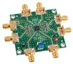
An evaluation board is also available.
Table 1. Passive Mixers
RF Frequency
(MHz)
500 to 1700
1200 to 2500
2200 to 2700
Single
Mixer
ADL5367
ADL5365
Single Mixer
and IF Amp
ADL5357
ADL5355
ADL5353
Dual Mixer
and IF Amp
ADL5358
ADL5356
ADL5354
The ADL5354 provides two switched LO paths that can be used
in time division duplex (TDD) applications where it is desirable
to ping-pong between two local oscillators. LO current can be
externally set using a resistor to minimize dc current
Rev. 0
Information furnished by Analog Devices is believed to be accurate and reliable. However, no
responsibility is assumed by Analog Devices for its use, nor for any infringements of patents or other
rights of third parties that may result from its use. Specifications subject to change without notice. No
license is granted by implication or otherwise under any patent or patent rights of Analog Devices.
Trademarks and registered trademarks are the property of their respective owners.
One Technology Way, P.O. Box 9106, Norwood, MA 02062-9106, U.S.A.
Tel: 781.329.4700
www.analog.com
Fax: 781.461.3113
©2011 Analog Devices, Inc. All rights reserved.
�ADL5354
TABLE OF CONTENTS
Features .............................................................................................. 1
Spur Tables ...................................................................................... 15
Applications....................................................................................... 1
5 V Performance......................................................................... 15
Functional Block Diagram .............................................................. 1
3.3 V Performance...................................................................... 15
General Description ......................................................................... 1
Circuit Description......................................................................... 16
Revision History ............................................................................... 2
RF Subsystem.............................................................................. 16
Specifications..................................................................................... 3
LO Subsystem ............................................................................. 16
5 V Performance........................................................................... 4
Applications Information .............................................................. 18
3.3 V Performance........................................................................ 4
Basic Connections...................................................................... 18
Absolute Maximum Ratings............................................................ 5
IF Port .......................................................................................... 18
ESD Caution.................................................................................. 5
Bias Resistor Selection ............................................................... 18
Pin Configuration and Function Descriptions............................. 6
Mixer VGS Control DAC .......................................................... 18
Typical Performance Characteristics ............................................. 7
Evaluation Board ............................................................................ 20
5 V Performance........................................................................... 7
Outline Dimensions ....................................................................... 22
3.3 V Performance...................................................................... 14
Ordering Guide .......................................................................... 22
REVISION HISTORY
2/11—Revision 0: Initial Version
Rev. 0 | Page 2 of 24
�ADL5354
SPECIFICATIONS
VS = 5 V, IS = 350 mA, TA = 25°C, fRF = 2535 MHz, fLO = 2332 MHz, LO power = 0 dBm, RF power = −10 dBm, R1 = R4 = 1.3 kΩ, R2 =
R5 = 1 kΩ, ZO = 50 Ω, VGS0 = VGS1 = VGS2 = 0 V, unless otherwise noted.
Table 2.
Parameter
RF INPUT INTERFACE
Return Loss
Input Impedance
RF Frequency Range
OUTPUT INTERFACE
Output Impedance
IF Frequency Range
DC Bias Voltage 1
LO INTERFACE
LO Power
Return Loss
Input Impedance
LO Frequency Range
POWER-DOWN (PWDN) INTERFACE 2
PWDN Threshold
Logic 0 Level
Logic 1 Level
PWDN Response Time
PWDN Input Bias Current
1
2
Test Conditions/Comments
Min
Tunable to >20 dB over a limited bandwidth
Typ
Unit
2700
dB
Ω
MHz
450
5.5
Ω||pF
MHz
V
20
50
2200
Differential impedance, f = 200 MHz
Externally generated
Max
230||0.75
30
3.3
−6
5.0
0
13
50
1750
+10
2670
1.0
0.4
1.4
Device enabled, IF output to 90% of its final level
Device disabled, supply current < 5 mA
Device enabled
Device disabled
Apply supply voltage from external circuit through choke inductors.
PWDN function is intended for use with VS ≤ 3.6 V only.
Rev. 0 | Page 3 of 24
160
230
0
70
dBm
dB
Ω
MHz
V
V
V
ns
ns
μA
μA
�ADL5354
5 V PERFORMANCE
VS = 5 V, IS = 350 mA, TA = 25°C, fRF = 2535 MHz, fLO = 2332 MHz, LO power = 0 dBm, RF power = −10 dBm, R1 = R4 = 1.3 kΩ, R2 = R5 = 1 kΩ,
VGS0 = VGS1 = VGS2 = 0 V, and ZO = 50 Ω, unless otherwise noted.
Table 3.
Parameter
DYNAMIC PERFORMANCE
Power Conversion Gain
Voltage Conversion Gain
SSB Noise Figure
Input Third-Order Intercept (IIP3)
Input Second-Order Intercept (IIP2)
Input 1 dB Compression Point (IP1dB)
LO-to-IF Leakage
LO-to-RF Leakage
RF-to-IF Isolation
IF/2 Spurious
IF/3 Spurious
IF Channel-to-Channel Isolation
POWER SUPPLY
Positive Supply Voltage
Quiescent Current
Total Quiescent Current
Test Conditions/Comments
Min
Including 4:1 IF port transformer and PCB loss
ZSOURCE = 50 Ω, differential ZLOAD = 200 Ω differential
fRF1 = 2534.5 MHz, fRF2 = 2535.5 MHz, fLO = 2332 MHz,
each RF tone at −10 dBm
fRF1 = 2535 MHz, fRF2 = 2585 MHz, fLO = 2332 MHz,
each RF tone at −10 dBm
Unfiltered IF output
−10 dBm input power
−10 dBm input power
4.75
LO supply
IF supply
VS = 5 V
Typ
Max
Unit
8.6
14.6
10.6
26.1
dB
dB
dB
dBm
50
dBm
10.6
−20.7
−37
−34
−73
−71
52
dBm
dBm
dBm
dBc
dBc
dBc
dB
5
170
180
350
5.25
V
mA
mA
mA
3.3 V PERFORMANCE
VS = 3.3 V, IS = 200 mA, TA = 25°C, fRF = 2535 MHz, fLO = 2332 MHz, LO power = 0 dBm, R9 = 226 Ω, R14 = 604 Ω, VGS0 = VGS1 = 0 V,
and ZO = 50 Ω, unless otherwise noted.
Table 4.
Parameter
DYNAMIC PERFORMANCE
Power Conversion Gain
Voltage Conversion Gain
SSB Noise Figure
Input Third-Order Intercept (IIP3)
Input Second-Order Intercept (IIP2)
Input 1 dB Compression Point (IP1dB)
POWER INTERFACE
Supply Voltage
Quiescent Current
Power-Down Current
Test Conditions/Comments
Min
Including 4:1 IF port transformer and PCB loss
ZSOURCE = 50 Ω, differential ZLOAD = 200 Ω differential
fRF1 = 2534.5 MHz, fRF2 = 2535.5 MHz, fLO = 2332 MHz, each
RF tone at −10 dBm
fRF1 = 2535 MHz, fRF2 = 2585 MHz, fLO = 2332 MHz, each RF
tone at −10 dBm
3.0
Resistor programmable
Device disabled
Rev. 0 | Page 4 of 24
Typ
Max
Unit
8
14
9.9
17.5
dB
dB
dB
dBm
49
dBm
7
dBm
3.3
200
300
3.6
V
mA
μA
�ADL5354
ABSOLUTE MAXIMUM RATINGS
Table 5.
Parameter
Supply Voltage, VS
RF Input Level
LO Input Level
MNOP, MNON, DVOP, DVON Bias
VGS2,VGS1,VGS0, LOSW, PWDN
Internal Power Dissipation
Thermal Characteristic θJA
Maximum Junction Temperature
Temperature Range
Operating
Storage
Lead Temperature (Soldering, 60 sec)
Stresses above those listed under Absolute Maximum Ratings
may cause permanent damage to the device. This is a stress
rating only; functional operation of the device at these or any
other conditions above those indicated in the operational
section of this specification is not implied. Exposure to absolute
maximum rating conditions for extended periods may affect
device reliability.
Rating
5.5 V
20 dBm
13 dBm
6.0 V
5.5 V
2.2 W
22°C/W
150°C
ESD CAUTION
−40°C to +85°C
−65°C to +150°C
260°C
Rev. 0 | Page 5 of 24
�ADL5354
36
35
34
33
32
31
30
29
28
VPOS
MNGM
COMM
MNON
MNOP
MNLE
VPOS
MNLG
NC
PIN CONFIGURATION AND FUNCTION DESCRIPTIONS
1
2
3
4
5
6
7
8
9
ADL5354
TOP VIEW
(Not to Scale)
27
26
25
24
23
22
21
LOI2
VGS2
VGS1
VGS0
LOSW
PWDN
VPOS
20 COMM
19 LOI1
NOTES
1. NC = NO CONNECT.
2. EXPOSED PAD MUST BE CONNECTED TO GROUND.
09118-002
DVGM
COMM
DVOP
DVON
DVLE
VPOS
DVLG
NC
VPOS 10
11
12
13
14
15
16
17
18
MNIN
MNCT
COMM
VPOS
COMM
VPOS
COMM
DVCT
DVIN
Figure 2. Pin Configuration
Table 6. Pin Function Descriptions
Pin No.
1
2
3, 5, 7, 12, 20, 34
4, 6, 10, 16, 21, 30, 36
8
9
11
13, 14
Mnemonic
MNIN
MNCT
COMM
VPOS
DVCT
DVIN
DVGM
DVOP, DVON
15
17
18, 28
19
22
DVLE
DVLG
NC
LOI1
PWDN
23
24, 25, 26
LOSW
VGS0, VGS1,
VGS2
LOI2
MNLG
MNLE
MNOP, MNON
27
29
31
32, 33
35
MNGM
EPAD
Description
RF Input for Main Channel. Internally matched to 50 Ω. Must be ac-coupled.
Center Tap for Main Channel Input Balun. Bypass to ground using low inductance capacitor.
Device Common (DC Ground).
Positive Supply Voltage.
Center Tap for Diversity Channel Input Balun. Bypass to ground using low inductance capacitor.
RF Input for Diversity Channel. Internally matched to 50 Ω. Must be ac-coupled.
Diversity Amplifier Bias Setting. Connect a 1.3 kΩ resistor to ground for typical operation.
Diversity Channel Differential Open-Collector Outputs. DVOP and DVON should be pulled up to
VCC using external inductors, see Figure 53 for details.
Diversity Channel IF Return. This pin must be grounded.
Diversity Channel LO Buffer Bias Setting. Connect a 1 kΩ resistor to ground for typical operation.
No Connect. Do not connect to this pin.
Local Oscillator Input 1. Internally matched to 50 Ω. Must be ac-coupled.
Power Down. Connect this pin to ground for normal operation. Connect pin to 3 V for disable
mode when using VPOS ≤ 3.6 V. PWDN pin must be grounded when VPOS > 3.6 V.
Local Oscillator Input Selection Switch. Set LOSW high to select LOI1 or set LOSW low to select LOI2.
Gate to Source Control Voltages. For typical operation, set VGS0, VGS1, and VGS2 to a low logic
level.
Local Oscillator Input 2. Internally matched to 50 Ω. Must be ac-coupled.
Main Channel LO Buffer Bias Setting. Connect a 1 kΩ resistor to ground for typical operation.
Main Channel IF Return. This pin must be grounded.
Main Channel Differential Open-Collector Outputs. Pull up MNOP and MNON to VCC by using
external inductors, see Figure 53 for details.
Main Amplifier Bias Setting. Connect a 1.3 kΩ resistor to ground for typical operation.
Exposed Paddle. Exposed pad must be connected to ground.
Rev. 0 | Page 6 of 24
�ADL5354
TYPICAL PERFORMANCE CHARACTERISTICS
5 V PERFORMANCE
VS = 5 V, IS = 350 mA, TA = 25°C, fRF = 2535 MHz, fLO = 2332 MHz, LO power = 0 dBm, RF power = −10 dBm, R1 = R4 = 1.3 kΩ, R2 = R5 = 1 kΩ,
ZO = 50 Ω, VGS0 = VGS1 = VGS2 = 0 V, unless otherwise noted.
400
60
390
58
56
TA = –40°C
54
360
TA = +25°C
350
340
TA = +85°C
52
48
330
46
320
44
310
42
2.25
2.30
2.35
2.40
2.45
2.50
2.55
2.60
2.65
2.70
RF FREQUENCY (GHz)
40
2.20
TA = +25°C
2.25
11
16
2.45
2.50
2.55
2.60
2.65
2.70
2.65
2.70
2.65
2.70
14
TA = –40°C
9
TA = +25°C
8
TA = +85°C
12
10
TA = –40°C
7
8
6
6
2.25
2.30
2.35
2.40
2.45
2.50
2.55
2.60
2.65
2.70
TA = +85°C
4
2.20
2.25
2.30
2.35
TA = +25°C
2.40
2.45
2.50
2.55
2.60
RF FREQUENCY (GHz)
Figure 4. Power Conversion Gain vs. RF Frequency
09118-007
INPUT P1dB (dBm)
10
09118-004
CONVERSION GAIN (dB)
18
RF FREQUENCY (GHz)
Figure 7. Input P1dB vs. RF Frequency
14
35
13
30
SSB NOISE FIGURE (dB)
TA = –40°C
25
TA = +25°C
20
TA = +85°C
15
10
12
TA = +85°C
11
TA = +25°C
10
TA = –40°C
9
8
7
2.25
2.30
2.35
2.40
2.45
2.50
2.55
2.60
RF FREQUENCY (GHz)
2.65
2.70
09118-005
INPUT IP3 (dBm)
2.40
Figure 6. Input IP2 vs. RF Frequency
12
5
2.20
2.35
RF FREQUENCY (GHz)
Figure 3. Supply Current vs. RF Frequency
5
2.20
2.30
TA = +85°C
6
2.20
2.25
2.30
2.35
2.40
2.45
2.50
2.55
2.60
RF FREQUENCY (GHz)
Figure 8. SSB Noise Figure vs. RF Frequency
Figure 5. Input IP3 vs. RF Frequency
Rev. 0 | Page 7 of 24
09118-008
300
2.20
TA = –40°C
50
09118-006
INPUT IP2 (dBm)
370
09118-003
SUPPLY CURRENT (mA)
380
�ADL5354
VS = 5 V, IS = 350 mA, TA = 25°C, fRF = 2535 MHz, fLO = 2332 MHz, LO power = 0 dBm, RF power = −10 dBm, R1 = R4 = 1.3 kΩ, R2 = R5 = 1 kΩ,
ZO = 50 Ω, VGS0 = VGS1 = VGS2 = 0 V, unless otherwise noted.
400
53
390
52
VS = 5.25V
370
51
INPUT IP2 (dBm)
SUPPLY CURRENT (mA)
380
360
VS = 5.00V
350
340
330
VS = 4.75V
VS = 5.25V
50
VS = 5.00V
49
VS = 4.75V
48
320
0
10
20
30
40
50
60
70
80
TEMPERATURE (°C)
46
–40 –30 –20 –10
09118-009
300
–40 –30 –20 –10
0
10
20
30
40
50
60
70
80
70
80
70
80
TEMPERATURE (°C)
Figure 9. Supply Current vs. Temperature
09118-012
47
310
Figure 12. Input IP2 vs. Temperature
9.4
15
14
9.2
INPUT P1dB (dBm)
8.8
8.6
VS = 5.25V
8.4
12
10
VS = 5.00V
VS = 4.75V
9
8
8.2
7
VS = 4.75V
8.0
0
10
20
30
40
50
60
70
80
TEMPERATURE (°C)
5
–40 –30 –20 –10
09118-010
7.8
–40 –30 –20 –10
0
10
20
30
40
50
60
TEMPERATURE (°C)
Figure 10. Power Conversion Gain vs. Temperature
09118-013
6
VS = 5.00V
Figure 13. Input P1dB vs. Temperature
12.0
29
11.5
28
11.0
26
SSB NOISE FIGURE (dB)
VS = 5.25V
27
VS = 5.00V
25
VS = 4.75V
24
23
10.5
VS = 5.25V
10.0
VS = 5.00V
9.5
VS = 4.75V
9.0
8.5
8.0
22
7.5
21
–40 –30 –20 –10
0
10
20
30
40
50
TEMPERATURE (°C)
60
70
80
7.0
–40 –30 –20 –10
09118-011
INPUT IP3 (dBm)
VS = 5.25V
11
0
10
20
30
40
50
60
TEMPERATURE (°C)
Figure 14. SSB Noise Figure vs. Temperature
Figure 11. Input IP3 vs. Temperature
Rev. 0 | Page 8 of 24
09118-014
CONVERSION GAIN (dB)
13
9.0
�ADL5354
VS = 5 V, IS = 350 mA, TA = 25°C, fRF = 2535 MHz, fLO = 2332 MHz, LO power = 0 dBm, RF power = −10 dBm, R1 = R4 = 1.3 kΩ,
R2 = R5 = 1 kΩ, ZO = 50 Ω, VGS0 = VGS1 = VGS2 = 0 V, unless otherwise noted.
400
60
390
58
56
INPUT IP2 (dBm)
54
360
350
TA = +25°C
340
TA = +85°C
50
46
320
44
310
42
80
130
180
230
280
330
380
430
IF FREQUENCY (MHz)
TA = +85°C
40
30
80
180
230
280
330
380
430
Figure 18. Input IP2 vs. IF Frequency
12
12
11
11
TA = +85°C
10
TA = –40°C
INPUT P1dB (dBm)
9
8
TA = +25°C
7
TA = +85°C
10
TA = –40°C
TA = +25°C
9
8
6
80
130
180
230
280
330
380
430
IF FREQUENCY (MHz)
6
30
09118-016
4
30
230
280
330
380
430
380
430
14
13
SSB NOISE FIGURE (dB)
35
TA = –40°C
25
TA = +25°C
TA = +85°C
15
12
11
10
9
8
80
130
180
230
280
330
IF FREQUENCY (MHz)
380
430
7
30
09118-017
10
30
180
Figure 19. Input P1dB vs. IF Frequency
40
20
130
IF FREQUENCY (MHz)
Figure 16. Power Conversion Gain vs. IF Frequency
30
80
09118-019
7
5
80
130
180
230
280
330
IF FREQUENCY (MHz)
Figure 17. Input IP3 vs. IF Frequency
Figure 20. SSB Noise Figure vs. IF Frequency
Rev. 0 | Page 9 of 24
09118-020
CONVERSION GAIN (dB)
130
IF FREQUENCY (MHz)
Figure 15. Supply Current vs. IF Frequency
INPUT IP3 (dBm)
TA = –40°C
48
330
300
30
TA = +25°C
52
09118-018
TA = –40°C
370
09118-015
SUPPLY CURRENT (mA)
380
�ADL5354
VS = 5 V, IS = 350 mA, TA = 25°C, fRF = 2535 MHz, fLO = 2332 MHz, LO power = 0 dBm, RF power = −10 dBm, R1 = R4 = 1.3 kΩ, R2 = R5 = 1 kΩ,
ZO = 50 Ω, VGS0 = VGS1 = VGS2 = 0 V, unless otherwise noted.
12
12.0
11.6
11
TA = +85°C
10.8
INPUT P1dB (dB)
CONVERSION GAIN (dB)
11.2
10
TA = –40°C
9
TA = +25°C
8
TA = +85°C
10.4
10.0
TA = +25°C
TA = –40°C
9.6
9.2
7
8.8
6
–4
–2
0
2
4
6
8
10
LO POWER (dBm)
8.0
–6
–4
30
–68
TA = +25°C
24
IF/2 SPURIOUS (dBc)
TA = +85°C
22
20
6
8
10
TA = –40°C
–70
–72
TA = +85°C
–74
–76
TA = +25°C
–78
18
–4
–2
0
2
4
6
8
10
LO POWER (dBm)
–80
2.20
09118-022
16
–6
4
2.25
2.30
2.35
2.40
2.45
2.50
2.55
2.60
2.65
2.70
RF FREQUENCY (GHz)
Figure 22. Input IP3 vs. LO Power
09118-025
INPUT IP3 (dBm)
–66
26
2
Figure 24. Input P1dB vs. LO Power
32
TA = –40°C
0
LO POWER (dBm)
Figure 21. Power Conversion Gain vs. LO Power
28
–2
09118-024
8.4
09118-021
5
–6
Figure 25. IF/2 Spurious vs. RF Frequency, RF Power = −10 dBm
58
–60
56
–62
IF/3 SPURIOUS (dBc)
52
TA = –40°C
TA = +25°C
50
TA = +85°C
48
46
–64
–66
TA = +85°C
–68
–70
44
–4
–2
0
2
4
6
LO POWER (dBm)
8
10
Figure 23. Input IP2 vs. LO Power
–74
2.20
2.25
2.30
2.35
TA = –40°C
2.40
2.45
2.50
2.55
2.60
2.65
2.70
RF FREQUENCY (GHz)
Figure 26. IF/3 Spurious vs. RF Frequency, RF Power = −10 dBm
Rev. 0 | Page 10 of 24
09118-026
40
–6
TA = +25°C
–72
42
09118-023
INPUT IP2 (dBm)
54
�ADL5354
MEAN = 8.6
SD = 0.28%
80
RESISTANCE (Ω)
DISTRIBUTION PERCENTAGE (%)
100
60
40
20
500
10
400
8
6
300
RESISTANCE
200
4
100
2
CAPACITANCE (pF)
VS = 5 V, IS = 350 mA, TA = 25°C, fRF = 2535 MHz, fLO = 2332 MHz, LO power = 0 dBm, RF power = −10 dBm, R1 = R4 = 1.3 kΩ, R2 = R5 = 1 kΩ,
ZO = 50 Ω, VGS0 = VGS1 = VGS2 = 0 V, unless otherwise noted.
8.5
8.6
8.7
CONVERSION GAIN (dB)
09118-027
8.4
0
30
180
230
280
330
380
430
0
Figure 30. IF Output Impedance (R Parallel, C Equivalent)
0
MEAN = 26.1
SD = 0.5%
–3
80
–6
RF RETURN LOSS (dB)
DISTRIBUTION PERCENTAGE (%)
130
IF FREQUENCY (MHz)
Figure 27. Conversion Gain Distribution
100
80
09118-030
CAPACITANCE
0
8.3
60
40
–9
–12
–15
–18
–21
20
24
25
26
27
28
INPUT IP3 (dBm)
–27
2.20
09118-028
0
23
2.25
2.40
2.45
2.50
2.55
2.60
2.65
2.70
2.40
2.45
2.50
Figure 31. RF Return Loss, Fixed IF
0
MEAN = 10.6
SD = 0.36%
–5
LO RETURN LOSS (dB)
80
60
40
–10
SELECTED
–15
UNSELECTED
–20
–25
20
0
10.0
10.3
10.6
10.9
INPUT P1dB (dBm)
11.2
–35
2.00
2.05
2.10
2.15
2.20
2.25
2.30
2.35
LO FREQUENCY (GHz)
Figure 32. LO Return Loss, Selected and Unselected
Figure 29. Input P1dB Distribution
Rev. 0 | Page 11 of 24
09118-132
–30
09118-029
DISTRIBUTION PERCENTAGE (%)
2.35
RF FREQUENCY (GHz)
Figure 28. Input IP3 Distribution
100
2.30
09118-031
–24
�ADL5354
VS = 5 V, IS = 350 mA, TA = 25°C, fRF = 2535 MHz, fLO = 2332 MHz, LO power = 0 dBm, RF power = −10 dBm, R1 = R4 = 1.3 kΩ,
R2 = R5 = 1 kΩ, ZO = 50 Ω, VGS0 = VGS1 = VGS2 = 0 V, unless otherwise noted.
60
–30
–32
LO-TO-RF LEAKAGE (dBm)
LO SWITCH ISOLATION (dB)
55
TA = –40°C
50
TA = +85°C
45
TA = +25°C
40
TA = –40°C
–34
–36
TA = +25°C
–38
TA = +85°C
–40
–42
–44
35
2.25
2.30
2.35
2.40
2.45
2.50
2.55
2.60
2.65
2.70
RF FREQUENCY (GHz)
–48
2.00
09118-133
0
–31
–5
TA = +85°C
2.20
2.25
2.30
2.35
2.40
2.45
2.50
TA = +25°C
–34
–35
TA = –40°C
–36
–37
–15
–25
–30
–40
–39
–45
2.30
2.35
2.40
2.45
2.50
2.55
2.60
2.65
2.70
RF FREQUENCY (GHz)
–50
2.00
2.10
2.15
2.20
2.25
2.30
2.35
2.40
2.45
2.50
2.45
2.50
Figure 37. 2 × LO Leakage vs. LO Frequency
–30
–5
–35
–10
–40
3 × LO LEAKAGE (dBm)
0
–15
TA = +25°C
–20
TA = +85°C
–25
2.05
LO FREQUENCY (GHz)
Figure 34 RF-to-IF Isolation vs. RF Frequency
TA = –40°C
2 × LO-TO-IF
–35
–38
2.25
2 × LO-TO-RF
–20
09118-037
2 × LO LEAKAGE (dBm)
–10
–33
09118-034
RF-TO-IF ISOLATION (dB)
–32
–30
–45
3 × LO-TO-RF
–50
–55
3 × LO-TO-IF
–60
–65
–35
2.05
2.10
2.15
2.20
2.25
2.30
2.35
2.40
LO FREQUENCY (GHz)
2.45
2.50
09118-035
LO-TO-IF LEAKAGE (dBm)
2.15
Figure 36. LO-to-RF Leakages vs. LO Frequency
–30
–40
2.00
2.10
LO FREQUENCY (GHz)
Figure 33. LO Switch Isolation vs. RF Frequency
–40
2.20
2.05
–70
2.00
2.05
2.10
2.15
2.20
2.25
2.30
2.35
2.40
LO FREQUENCY (GHz)
Figure 38. 3 × LO Leakage vs. LO Frequency
Figure 35. LO-to-IF Leakage vs. LO Frequency
Rev. 0 | Page 12 of 24
09118-038
30
2.20
09118-036
–46
�ADL5354
18
0.30
9
16
0.25
8
14
7
12
6
10
2.35
2.40
2.45
2.50
2.55
SUPPLY CURRENT (mA)
0
0.6
26
14
23
20
12
17
10
8
6
2.20
INPUT IP3 (dBm)
16
2.25
2.30
2.35
2.40
2.45
2.50
2.55
VGS = 000
VGS = 011 14
VGS = 100
VGS = 110
11
2.60 2.65 2.70
RF FREQUENCY (GHz)
13
29
INPUT IP3
26
SSB NOISE FIGURE
23
12
11
20
10
9
17
CONVERSION GAIN
8
14
7
11
6
0.6
0.7
0.8
0.9
1.0
1.1
1.2
1.3
1.4
1.5
LO BIAS RESISTOR VALUE (kΩ)
1.6
1.7
8
1.8
1.1
1.2
1.3
1.4
1.5
1.6
1.7
1.8
30
INPUT IP3
15
27
14
24
13
21
18
12
SSB NOISE FIGURE
11
15
12
10
9
9
CONVERSION GAIN
8
6
7
3
6
0.6
0.7
0.8
0.9
1.0
1.1
1.2
1.3
1.4
1.5
1.6
1.7
0
1.8
IF BIAS RESISTOR VALUE (kΩ)
62
IF CHANNEL-TO-CHANNEL ISOLATION (dB)
32
INPUT IP3 (dBm)
14
1.0
Figure 43. Power Conversion Gain, SSB Noise Figure, and Input IP3 vs. IF Bias
Resistor Value
09118-041
CONVERSION GAIN AND SSB NOISE FIGURE (dB)
Figure 40. Input P1dB and Input IP3 vs. RF Frequency for Various VGS Settings
0.9
16
09118-040
INPUT P1dB (dBm)
29
0.8
Figure 42. LO and IF Supply Current vs. IF and LO Bias Resistor Value
CONVERSION GAIN AND SSB NOISE FIGURE (dB)
32
0.7
BIAS RESISTOR VALUE (kΩ)
Figure 39. Power Conversion Gain and SSB Noise Figure vs. RF Frequency for
Various VGS Settings
18
0.10
0.05
RF FREQUENCY (GHz)
20
LO BIAS SUPPLY CURRENT
09118-142
2.30
0.15
INPUT IP3 (dBm)
2.25
0.20
09118-042
4
2.20
VGS = 000
8
VGS = 011
VGS = 100
VGS = 110
6
2.60 2.65 2.70
IF BIAS SUPPLY CURRENT
Figure 41. Power Conversion Gain, SSB Noise Figure, and Input IP3 vs. LO Bias
Resistor Value
Rev. 0 | Page 13 of 24
TA = –40°C
60
TA = +25°C
58
56
54
TA = +85°C
52
50
2.20
2.25
2.30
2.35
2.40
2.45
2.50
2.55
2.60
2.65
2.70
RF FREQUENCY (GHz)
Figure 44. IF Channel-to-Channel Isolation vs. RF Frequency
09118-043
5
SSB NOISE FIGURE (dB)
10
09118-039
CONVERSION GAIN (dB)
VS = 5 V, IS = 350 mA, TA = 25°C, fRF = 2535 MHz, fLO = 2332 MHz, LO power = 0 dBm, RF power = −10 dBm, R1 = R4 = 1.3 kΩ, R2 = R5 = 1 kΩ,
ZO = 50 Ω, VGS0 = VGS1 = VGS2 = 0 V, unless otherwise noted.
�ADL5354
3.3 V PERFORMANCE
VS = 3.3 V, IS = 200 mA, TA = 25°C, fRF = 2535 MHz, fLO = 2332 MHz, LO power = 0 dBm, R9 = 226 Ω, R14 = 604 Ω, VGS0 = VGS1 = 0 V,
and ZO = 50 Ω, unless otherwise noted.
208
60
TA = +25°C
206
50
TA = –40°C
202
INPUT IP2 (dBm)
SUPPLY CURRENT (mA)
204
200
198
TA = +25°C
196
194
TA = +85°C
192
40
TA = +85°C
30
TA = –40°C
20
10
2.25
2.30
2.35
2.40
2.45
2.50
2.55
2.60
2.65
2.70
RF FREQUENCY (GHz)
0
2.20
09118-044
8
13
6
7
TA = +85°C
3
1
2.45
2.50
2.55
2.60
2.65
2.70
TA = +25°C
TA = +85°C
2
0
–2
–4
–6
–1
TA = –40°C
–8
–3
2.25
2.30
2.35
2.40
2.45
2.50
2.55
2.60
2.65
2.70
RF FREQUENCY (GHz)
–10
2.20
09118-045
–5
2.20
2.40
4
TA = –40°C
INPUT P1dB (dBm)
CONVERSION GAIN (dB)
11
TA = +25°C
2.35
Figure 48. Input IP2 vs. RF Frequency at 3.3 V
15
5
2.30
RF FREQUENCY (GHz)
Figure 45. Supply Current vs. RF Frequency at 3.3 V
9
2.25
2.25
2.30
2.35
2.40
2.45
2.50
2.55
2.60
2.65
2.70
RF FREQUENCY (GHz)
09118-048
188
2.20
09118-047
190
Figure 49. Input P1dB vs. RF Frequency at 3.3 V
Figure 46. Power Conversion Gain vs. RF Frequency at 3.3 V
25
22
20
20
SSB NOISE FIGURE (dB)
15
TA = +25°C
TA = +85°C
10
18
16
14
12
TA = +85°C
10
5
TA = +25°C
0
2.20
2.25
2.30
2.35
2.40
2.45
2.50
2.55
2.60
RF FREQUENCY (GHz)
2.65
2.70
Figure 47. Input IP3 vs. RF Frequency at 3.3 V
6
2.20
2.25
2.30
2.35
2.40
2.45
2.50
2.55
2.60
2.65
RF FREQUENCY (GHz)
Figure 50. SSB Noise Figure vs. RF Frequency at 3.3 V
Rev. 0 | Page 14 of 24
2.70
09118-049
TA = –40°C
8
09118-046
INPUT IP3 (dBm)
TA = –40°C
�ADL5354
SPUR TABLES
All spur tables are (N × fRF) − (M × fLO) and were measured using the standard evaluation board. Mixer spurious products are measured
in dBc from the IF output power level. Data was measured only for frequencies less than 6 GHz. Typical noise floor of the measurement
system = −100 dBm.
5 V PERFORMANCE
VS = 5 V, IS = 350 mA, TA = 25°C, fRF = 2500 MHz, fLO = 2297 MHz, LO power = 0 dBm, RF power = −10 dBm, VGS0 = VGS1 = VGS2 = 0 V,
and ZO = 50 Ω, unless otherwise noted.
M
0
0
1
2
3
4
5
6
7
N
8
9
10
11
12
13
14
15
−41.5
−92.6
1
−19.7
0.00
−95.3