1 MHz to 10 GHz, 62 dB Dual Log
Detector/Controller
ADL5519
Data Sheet
VPSA
ADJA
VPSR
TEMP
CLPA
VSTA
23
22
21
20
19
18
17
ADL5519
TEMP
INLA 26
16 NC
15 OUTA
CHANNEL A
LOG DETECTOR
14 FBKA
COMR 27
PWDN 28
COMR 29
COMR 30
13 OUTP
OUTA
OUTB
12 OUTN
11 FBKB
CHANNEL B
LOG DETECTOR
10 OUTB
INHB 32
9 NC
3
4
5
6
7
8
VPSB
ADJB
VREF
VLVL
CLPB
VSTB
06198-001
2
COMR
BIAS
1
COMR
RF transmitter power amplifier linearization and
gain/power control
Power monitoring in radio link transmitters
Dual-channel wireless infrastructure radios
Antenna VSWR monitor
RSSI measurement in base stations, WLAN, WiMAX, radar
24
INHA 25
INLB 31
APPLICATIONS
COMR
FUNCTIONAL BLOCK DIAGRAM
Wide bandwidth: 1 MHz to 10 GHz
Dual-channel and channel difference output ports
Integrated accurate scaled temperature sensor
62 dB dynamic range (±3 dB)
>50 dB with ±1 dB up to 8 GHz
Stability over temperature: ±0.5 dB (−40oC to +85oC)
Low noise detector/controller outputs
Pulse response time: 6 ns/8 ns (fall time/rise time)
Supply operation: 3.3 V to 5.5 V @ 60 mA
Fabricated using high speed SiGe process
Small footprint, 5 mm × 5 mm, 32-lead LFCSP
Operating temperature range: −40oC to +125oC
COMR
FEATURES
Figure 1.
GENERAL DESCRIPTION
The ADL5519 is a dual-demodulating logarithmic amplifier that
incorporates two AD8317s. It can accurately convert an RF
input signal into a corresponding decibel-scaled output. The
ADL5519 provides accurately scaled, independent, logarithmic
output voltages for both RF measurement channels. The device
has two additional output ports, OUTP and OUTN, that
provide the measured differences between the OUTA and
OUTB channels. The on-chip channel matching makes the log
amp outputs insensitive to temperature and process variations.
The temperature sensor pin provides a scaled voltage that is
proportional to the temperature over the operating temperature
range of the device.
The ADL5519 maintains accurate log conformance for signals
from 1 MHz to 8 GHz and provides useful operation to 10 GHz.
The ±3 dB dynamic range is typically 62 dB and has a ±1 dB
dynamic range of >50 dB (re: 50 Ω). The ADL5519 has a response
time of 6 ns/8 ns (fall time/rise time) that enables RF burst detection to a pulse rate of greater than 50 MHz. The device provides
unprecedented logarithmic intercept stability vs. ambient
Rev. C
temperature conditions. A supply of 3.3 V to 5.5 V is required
to power the device. Current consumption is typically 60 mA,
and it decreases to less than 1 mA when the device is disabled.
The device is capable of supplying four log amp measurements
simultaneously. Linear-in-dB measurements are provided at
OUTA and OUTB with conveniently scaled slopes of −22 mV/dB.
The log amp difference between OUTA and OUTB is available
as differential or single-ended signals at OUTP and OUTN. An
optional voltage applied to VLVL provides a common-mode
reference level to offset OUTP and OUTN above ground. The
broadband output pins can support many system solutions.
Any of the ADL5519 output pins can be configured to provide
a control voltage to a variable gain amplifier (VGA). Special
attention has been paid to minimize the broadband noise of the
output pins so that they can be used for controller applications.
The ADL5519 is fabricated on a SiGe bipolar IC process and is
available in a 5 mm × 5 mm, 32-lead LFCSP with an operating
temperature range of −40°C to +125°C.
Document Feedback
Information furnished by Analog Devices is believed to be accurate and reliable. However, no
responsibility is assumed by Analog Devices for its use, nor for any infringements of patents or other
rights of third parties that may result from its use. Specifications subject to change without notice.
No license is granted by implication or otherwise under any patent or patent rights of Analog
Devices. Trademarks and registered trademarks are the property of their respective owners.
One Technology Way, P.O. Box 9106, Norwood, MA 02062-9106, U.S.A.
Tel: 781.329.4700 ©2008–2020 Analog Devices, Inc. All rights reserved.
Technical Support
www.analog.com
�ADL5519
Data Sheet
TABLE OF CONTENTS
Features .............................................................................................. 1
Basis for Error Calculations ...................................................... 23
Applications ...................................................................................... 1
Device Calibration ..................................................................... 24
Functional Block Diagram .............................................................. 1
Adjusting Accuracy Through Choice of Calibration Points..... 24
General Description ......................................................................... 1
Temperature Compensation Adjustment .............................. 25
Revision History ............................................................................... 2
Altering the Slope ....................................................................... 26
Specifications .................................................................................... 3
Channel Isolation ....................................................................... 26
Absolute Maximum Ratings ........................................................... 9
Output Filtering ......................................................................... 27
ESD Caution.................................................................................. 9
Package Considerations ............................................................ 27
Pin Configuration and Function Descriptions .......................... 10
Operation Above 8 GHz ........................................................... 27
Typical Performance Characteristics ........................................... 11
Applications Information ............................................................. 28
Theory of Operation ...................................................................... 19
Measurement Mode ................................................................... 28
Using the ADL5519 ........................................................................ 20
Controller Mode ......................................................................... 28
Basic Connections ...................................................................... 20
Automatic Gain Control ........................................................... 30
Input Signal Coupling ............................................................... 20
Gain-Stable Transmitter/Receiver ........................................... 32
Temperature Sensor Interface .................................................. 22
Measuring VSWR ...................................................................... 34
VREF Interface ........................................................................... 22
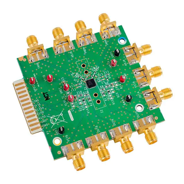
Evaluation Board ............................................................................ 36
Power-Down Interface .............................................................. 22
Configuration Options .............................................................. 36
Setpoint Interface—VSTA, VSTB ............................................ 22
Evaluation Board Schematic and Artwork ............................. 37
Output Interface—OUTA, OUTB ........................................... 22
Outline Dimensions ....................................................................... 39
Difference Output—OUTP, OUTN ........................................ 23
Ordering Guide .......................................................................... 39
Description of Characterization ............................................... 23
REVISION HISTORY
8/2020—Rev. B to Rev. C
Changes to Figure 38 ..................................................................... 16
Changes to Figure 71 ..................................................................... 35
4/2009—Rev. 0 to Rev. A
Changes to Table 5 ......................................................................... 36
Changes to Figure 72 ..................................................................... 37
9/2017—Rev. A to Rev. B
Changes to Figure 2........................................................................ 10
Updated Outline Dimensions ....................................................... 39
Changes to Ordering Guide .......................................................... 39
1/2008—Revision 0: Initial Version
Rev. C | Page 2 of 39
�Data Sheet
ADL5519
SPECIFICATIONS
Supply voltage, VP = VPSR = VPSA = VPSB = 5 V, CLPF = 1000 pF, TA = 25°C, 50 Ω termination resistor at INHA, INHB, unless otherwise
noted.
Table 1.
Parameter
Conditions
SIGNAL INPUT INTERFACE
Specified Frequency Range
DC Common-Mode Voltage
MEASUREMENT MODE,
100 MHz OPERATION
INHA, INHB (Pin 25, Pin 32)
Min
Temperature Sensitivity
Input A-to-Input B Isolation
Input A-to-OUTB Isolation
Input B-to-OUTA Isolation
MEASUREMENT MODE,
900 MHz OPERATION
Unit
10
VP − 0.7
GHz
V
1670||0.47
51
42
−1
−52
−22
22
0.7
1.37
50
44
Ω||pF
dB
dB
dBm
dBm
mV/dB
dBm
V
V
dB
dB
±0.25
+0.16
−0.6
dB
dB
dB
±0.25
dB
±0.4
dB
±0.25
dB
±0.45
dB
80
60
dB
dB
60
dB
925||0.54
54
49
−2
−56
−22
20.3
Ω||pF
dB
dB
dBm
dBm
mV/dB
dBm
ADJA (Pin 21) = 0.65 V, ADJB (Pin 4) = 0.7 V; OUTA, OUTB
(Pin 15, Pin 10) shorted to VSTA, VSTB (Pin 17, Pin 8);
OUTP, OUTN (Pin 13, Pin 12) shorted to FBKA, FBKB
(Pin 14, Pin 11), respectively; sinusoidal input signal;
error referred to best-fit line using linear regression
between PINHA, PINHB = −40 dBm and −10 dBm
−40°C < TA < +85°C
±1 dB error
±1 dB error
OUTA, OUTB @ PINHA, PINHB = −16 dBm
OUTA, OUTB @ PINHA, PINHB = −40 dBm
±1 dB error
−40°C < TA < +85°C
Deviation from OUTA, OUTB @ 25°C
−40°C < TA < +85°C, PINHA, PINHB = −16 dBm
25°C < TA < 85°C, PINHA, PINHB = −40 dBm
−40°C < TA < +25°C, PINHA, PINHB = −40 dBm
Distribution of OUTP, OUTN from 25°C
25°C < TA < 85°C, PINHA = −16 dBm, PINHB = −30 dBm,
typical error = −0.09 dB
−40°C < TA < +25°C, PINHA = −16 dBm, PINHB = −30 dBm,
typical error = 0.25 dB
25°C < TA < 85°C, PINHA = −40 dBm, PINHB = −30 dBm,
typical error = 0.05 dB
−40°C < TA < +25°C, PINHA = −40 dBm, PINHB = −30 dBm,
typical error = −0.23 dB
Frequency separation = 1 kHz, PINHA = −50 dBm,
PINHA – PINHB when OUTB/Slope = 1 dB
Frequency separation = 1 kHz, PINHB = −50 dBm,
PINHB – PINHA when OUTA/Slope = 1 dB
ADJA = 0.6 V, ADJB = 0.65 V; OUTA, OUTB shorted to
VSTA, VSTB; OUTP, OUTN shorted to FBKA, FBKB, respectively;
sinusoidal input signal; error referred to best fit line using
linear regression between PINHA, PINHB = −40 dBm and
−10 dBm
Input Impedance
OUTA, OUTB ± 1 dB Dynamic Range
OUTA, OUTB Maximum Input Level
OUTA, OUTB Minimum Input Level
OUTA, OUTB, OUTP, OUTN Slope1
OUTA, OUTB Intercept1
Max
0.001
Input Impedance
OUTA, OUTB ± 1 dB Dynamic Range
OUTA, OUTB Maximum Input Level
OUTA, OUTB Minimum Input Level
OUTA, OUTB, OUTP, OUTN Slope1
OUTA, OUTB Intercept1
Output Voltage (High Power In)
Output Voltage (Low Power In)
OUTP, OUTN Dynamic Gain Range
Typ
−40°C < TA < +85°C
±1 dB error
±1 dB error
Rev. C | Page 3 of 39
�ADL5519
Parameter
Output Voltage (High Power In)
Output Voltage (Low Power In)
OUTP, OUTN Dynamic Gain Range
Temperature Sensitivity
Input A-to-Input B Isolation
Input A-to-OUTB Isolation
Input B-to-OUTA Isolation
MEASUREMENT MODE,
1.9 GHz OPERATION
Data Sheet
Conditions
Min
OUTA, OUTB @ PINHA, PINHB = −10 dBm
OUTA, OUTB @ PINHA, PINHB = −40 dBm
±1 dB error
−40°C < TA < +85°C
Deviation from OUTA, OUTB @ 25°C
−40°C < TA < +85°C, PINHA, PINHB = −16 dBm
25°C < TA < 85°C, PINHA, PINHB = −40 dBm
−40°C < TA < +25°C, PINHA, PINHB = −40 dBm
Distribution OUTP, OUTN from 25°C
25°C < TA < 85°C, PINHA = −16 dBm, PINHB = −30 dBm,
typical error = −0.08 dB
−40°C < TA < +25°C, PINHA = −16 dBm, PINHB = −30 dBm
typical error = 0.3 dB
25°C < TA < 85°C, PINHA = −40 dBm, PINHB = −30 dBm,
typical error = 0.17 dB
−40°C < TA < +25°C, PINHA = −40 dBm, PINHB = −30 dBm,
typical error = −0.19 dB
Frequency separation = 1 kHz, PINHA = −50 dBm,
PINHA – PINHB when OUTB/Slope = 1 dB
Frequency separation = 1 kHz, PINHB = −50 dBm,
PINHB – PINHA when OUTA/Slope = 1 dB
ADJA = 0.5 V, ADJB = 0.55 V; OUTA, OUTB shorted to
VSTA, VSTB; OUTP, OUTN shorted to FBKA, FBKB, respectively;
sinusoidal input signal; error referred to best fit line using
linear regression between PINHA, PINHB = −40 dBm and
−10 dBm
Input Impedance
OUTA, OUTB ± 1 dB Dynamic Range
OUTA, OUTB Maximum Input Level
OUTA, OUTB Minimum Input Level
OUTA, OUTB, OUTP, OUTN Slope1
OUTA, OUTB Intercept1
Output Voltage (High Power In)
Output Voltage (Low Power In)
OUTP, OUTN Dynamic Gain Range
Temperature Sensitivity
Input A-to-Input B Isolation
Input A-to-OUTB Isolation
Input B-to-OUTA Isolation
−40°C < TA < +85°C
±1 dB error
±1 dB error
OUTA, OUTB @ PINHA, PINHB = −10 dBm
OUTA, OUTB @ PINHA, PINHB = −40 dBm
±1 dB error
−40°C < TA < +85°C
Deviation from OUTA, OUTB @ 25°C
−40°C < TA < +85°C, PINHA, PINHB = −16 dBm
25°C < TA < 85°C, PINHA, PINHB = −40 dBm
−40°C < TA < +25°C, PINHA, PINHB = −40 dBm
Distribution of OUTP, OUTN from 25°C
25°C < TA < 85°C, PINHA = −16 dBm, PINHB = −30 dBm,
typical error = −0.07 dB
−40°C < TA < +25°C, PINHA = −16 dBm, PINHB = −30 dBm,
typical error = 0.23 dB
25°C < TA < 85°C, PINHA = −40 dBm, PINHB = −30 dBm,
typical error = 0.16 dB
−40°C < TA < +25°C, PINHA = −40 dBm, PINHB = −30 dBm,
typical error = −0.22 dB
Frequency separation = 1 kHz, PINHA = −50 dBm,
PINHA – PINHB when OUTB/Slope = 1 dB
Frequency separation = 1 kHz, PINHB = −50 dBm,
PINHB – PINHA when OUTA/Slope = 1 dB
Rev. C | Page 4 of 39
Typ
Max
Unit
0.67
1.34
55
48
V
V
dB
dB
±0.25
+0.25
−0.5
dB
dB
dB
±0.25
dB
±0.4
dB
±0.25
dB
±0.4
dB
75
50
dB
dB
50
dB
525||0.36
55
49
−4
−59
−22
18
0.62
1.28
55
48
Ω||pF
dB
dB
dBm
dBm
mV/dB
dBm
V
V
dB
dB
±0.2
+0.25
−0.5
dB
dB
dB
±0.3
dB
±0.4
dB
±0.3
dB
±0.4
dB
65
46
dB
dB
46
dB
�Data Sheet
ADL5519
Parameter
Conditions
MEASUREMENT MODE,
2.2 GHz OPERATION
ADJA = 0.48 V, ADJB = 0.6 V; OUTA, OUTB shorted to
VSTA, VSTB; OUTP, OUTN shorted to FBKA, FBKB, respectively;
sinusoidal input signal; error referred to best fit line using
linear regression between PINHA, PINHB = −40 dBm and
−10 dBm
Min
Input Impedance
OUTA, OUTB ± 1 dB Dynamic Range
OUTA, OUTB Maximum Input Level
OUTA, OUTB Minimum Input Level
OUTA, OUTB, OUTP, OUTN Slope1
OUTA, OUTB Intercept1
Output Voltage (High Power In)
Output Voltage (Low Power In)
OUTP, OUTN Dynamic Gain Range
Temperature Sensitivity
Input A-to-Input B Isolation
Input A-to-OUTB Isolation
Input B-to-OUTA Isolation
MEASUREMENT MODE,
3.6 GHz OPERATION
−40°C < TA < +85°C
±1 dB error
±1 dB error
OUTA, OUTB @ PINHA, PINHB = −10 dBm
OUTA, OUTB @ PINHA, PINHB = −40 dBm
±1 dB error
−40°C < TA < +85°C
Deviation from OUTA, OUTB @ 25°C
−40°C < TA < +85°C, PINHA, PINHB = −16 dBm
25°C < TA < 85°C, PINHA, PINHB = −40 dBm
−40°C < TA < +25°C, PINHA, PINHB = −40 dBm
Distribution of OUTP, OUTN from 25°C
25°C < TA < 85°C, PINHA = −16 dBm, PINHB = −30 dBm,
typical error = −0.07 dB
−40°C < TA < +25°C, PINHA = −16 dBm, PINHB = −30 dBm,
typical error = 0.25 dB
25°C < TA < 85°C, PINHA = −40 dBm, PINHB = −30 dBm,
typical error = 0.17 dB
−40°C < TA < +25°C, PINHA = −40 dBm, PINHB = −30 dBm
typical error = −0.22dB
Frequency separation = 1 kHz, PINHA = −50 dBm,
PINHA – PINHB when OUTB/Slope = 1 dB
Frequency separation = 1 kHz, PINHB = −50 dBm,
PINHB – PINHA when OUTA/Slope = 1 dB
ADJA = 0.35 V ADJB = 0.42; OUTA, OUTB shorted to
VSTA, VSTB; OUTP, OUTN shorted to FBKA, FBKB, respectively;
sinusoidal input signal; error referred to best fit line using
linear regression between PINHA, PINHB = −40 dBm and
−10 dBm
Input Impedance
OUTA, OUTB ± 1 dB Dynamic Range
OUTA, OUTB Maximum Input Level
OUTA, OUTB Minimum Input Level
OUTA, OUTB, OUTP, OUTN Slope1
OUTA, OUTB Intercept1
Output Voltage (High Power In)
Output Voltage (Low Power In)
OUTP, OUTN Dynamic Gain Range
−40°C < TA < +85°C
±1 dB error
±1 dB error
OUTA, OUTB @ PINHA, PINHB = −10 dBm
OUTA, OUTB @ PINHA, PINHB = −40 dBm
±1 dB error
−40°C < TA < +85°C
Rev. C | Page 5 of 39
Typ
Max
Unit
408||0.34
55
50
−5
−60
−22
16.9
0.6
1.26
56
40
Ω||pF
dB
dB
dBm
dBm
mV/dB
dBm
V
V
dB
dB
±0.28
+0.3
−0.5
dB
dB
dB
±0.25
dB
±0.4
dB
±0.25
dB
±0.4
dB
60
46
dB
dB
46
dB
187||0.66
54
44
−4
−58
−22.5
17
0.62
1.31
52
42
Ω||pF
dB
dB
dBm
dBm
mV/dB
dBm
V
V
dB
dB
�ADL5519
Parameter
Temperature Sensitivity
Input A-to-Input B Isolation
Input A-to-OUTB Isolation
Input B-to-OUTA Isolation
MEASUREMENT MODE,
5.8 GHz OPERATION
Data Sheet
Conditions
Min
Deviation from OUTA, OUTB @ 25°C
−40°C < TA < +85°C, PINHA, PINHB = −16 dBm
25°C < TA < 85°C, PINHA, PINHB = −40 dBm
−40°C < TA < +25°C, PINHA, PINHB = −40 dBm
Distribution of OUTP, OUTN from 25°C
25°C < TA < 85°C, PINHA = −16 dBm, PINHB = −30 dBm,
typical error = −0.07 dB
−40°C < TA < +25°C, PINHA = −16 dBm, PINHB = −30 dBm,
typical error = 0.27 dB
25°C < TA < 85°C, PINHA = −40 dBm, PINHB = −30 dBm,
typical error = 0.31 dB
−40°C < TA < +25°C, PINHA = −40 dBm, PINHB = −30 dBm,
typical error = −0.14 dB
Frequency separation = 1 kHz, PINHA = −50 dBm,
PINHA – PINHB when OUTB/Slope = 1 dB
Frequency separation = 1 kHz, PINHB = −50 dBm,
PINHB – PINHA when OUTA/Slope = 1 dB
ADJA = 0.58 V, ADJB = 0.7 V; OUTA, OUTB shorted to
VSTA, VSTB; OUTP, OUTN shorted to FBKA, FBKB respectively;
sinusoidal input signal; error referred to best fit line using
linear regression between PINHA, PINHB = −40 dBm and
−20 dBm
Input Impedance
OUTA, OUTB ± 1 dB Dynamic Range
OUTA, OUTB Maximum Input Level
OUTA, OUTB Minimum Input Level
OUTA, OUTB, OUTP, OUTN Slope1
OUTA, OUTB Intercept1
Output Voltage (High Power In)
Output Voltage (Low Power In)
OUTP, OUTN Dynamic Gain Range
Temperature Sensitivity
Input A-to-Input B Isolation
Input A-to-OUTB Isolation
Input B-to-OUTA Isolation
−40°C < TA < +85°C
±1 dB error
±1 dB error
OUTA, OUTB @ PINHA, PINHB = −10 dBm
OUTA, OUTB @ PINHA, PINHB = −40 dBm
±1 dB error
−40°C < TA < +85°C
Deviation from OUTA, OUTB @ 25°C
−40°C < TA < +85°C, PINHA, PINHB = −16dBm
25°C < TA < 85°C, PINHA, PINHB = −40 dBm
−40°C < TA < +25°C, PINHA, PINHB = −40 dBm
Distribution of OUTP, OUTN from 25°C
25°C < TA < 85°C, PINHA = −16 dBm, PINHB = −30 dBm,
typical error = 0.02 dB
−40°C < TA < +25°C, PINHA = −16 dBm, PINHB = −30 dBm,
typical error = 0.25 dB
25°C < TA < 85°C, PINHA = −40 dBm, PINHB = −30 dBm,
typical error = 0.13 dB
−40°C < TA < +25°C, PINHA = −40 dBm, PINHB = −30 dBm,
typical error = 0.06 dB
Frequency separation = 1 kHz, PINHA = −50 dBm,
PINHA – PINHB when OUTB/Slope = 1 dB
Frequency separation = 1 kHz, PINHB = −50 dBm,
PINHB – PINHA when OUTA/Slope = 1 dB
Rev. C | Page 6 of 39
Typ
Max
Unit
±0.4
+0.6
−0.45
dB
dB
dB
±0.25
dB
±0.45
dB
±0.3
dB
±0.5
dB
40
20
dB
dB
20
dB
28||1.19
53
45
−2
−55
−22.5
20
0.68
1.37
53
46
Ω||pF
dB
dB
dBm
dBm
mV/dB
dBm
V
V
dB
dB
±0.25
+0.25
−0.4
dB
dB
dB
±0.3
dB
±0.4
dB
±0.3
dB
±0.5
dB
45
48
dB
dB
48
dB
�Data Sheet
ADL5519
Parameter
Conditions
MEASUREMENT MODE,
8 GHz OPERATION
ADJA = 0.72 V, ADJB = 0.82 V to GND; OUTA, OUTB shorted
to VSTA, VSTB; OUTP, OUTN shorted to FBKA, FBKB,
respectively; sinusoidal input signal; error referred to best
fit line using linear regression between PINHA, PINHB = −40 dBm
and −20 dBm
Min
Input Impedance
OUTA, OUTB ± 1 dB Dynamic Range
OUTA, OUTB Maximum Input Level
OUTA, OUTB Minimum Input Level
OUTA, OUTB, OUTP, OUTN Slope1
OUTA, OUTB Intercept1
Output Voltage (High Power In)
Output Voltage (Low Power In)
OUTP, OUTN Dynamic Gain Range
Temperature Sensitivity
Input A-to-Input B Isolation
Input A-to-OUTB Isolation
Input B-to-OUTA Isolation
OUTPUT INTERFACE
OUTA, OUTB Voltage Range
OUTP, OUTN Voltage Range
Source/Sink Current
Capacitance Drive
Output Noise
Fall Time
Rise Time
−40°C < TA < +85°C
±1 dB error
±1 dB error
OUTA, OUTB @ PINHA, PINHB = −10 dBm
OUTA, OUTB @ PINHA, PINHB = −40 dBm
±1 dB error
−40°C < TA < +85°C
Deviation from OUTA, OUTB @ 25°C
−40°C < TA < +85°C, PINHA, PINHB = −16 dBm
25°C < TA < 85°C, PINHA, PINHB = −40 dBm
−40°C < TA < +25°C, PINHA, PINHB = −40 dBm
Distribution of OUTP, OUTN from 25°C
25°C < TA < 85°C, PINHA = −16 dBm, PINHB = −30 dBm,
typical error = 0.2dB
−40°C < TA < +25°C, PINHA = −16 dBm, PINHB = −30 dBm,
typical error = 0.09dB
25°C < TA < 85°C, PINHA = −40 dBm, PINHB = −30 dBm,
typical error = −0.07dB
−40°C < TA < +25°C, PINHA = −40 dBm, PINHB = −30 dBm,
typical error = 0.17 dB
Frequency separation = 1 kHz, PINHA = −50 dBm,
PINHA – PINHB when OUTB/Slope = 1 dB
Frequency separation = 1 kHz, PINHB = −50 dBm,
PINHB – PINHA when OUTA/Slope = 1 dB
OUTA, OUTB; OUTP, OUTN
VSTA, VSTB = 1.7 V, RF in = open
VSTA, VSTB = 0 V, RF in = open
FBKA, FBKB = open and OUTA < OUTB, RL ≥ 240 Ω to ground
FBKA, FBKB = open and OUTA > OUTB, RL ≥ 240 Ω to ground
Output held at 1 V to 1% change
INHA, INHB = 2.2 GHz, −10 dBm, fNOISE = 100 kHz,
CLPA, CLPB = open
Input level = no signal to −10 dBm, 80% to 20%,
CLPA, CLPB = 10 pF
Input level = no signal to −10 dBm, 80% to 20%,
CLPA, CLPB = open
Input level = −10 dBm to no signal, 20% to 80%,
CLPA, CLPB = 10 pF
Input level = −10 dBm to no signal, 20% to 80%,
CLPA, CLPB = open
Video Bandwidth
(or Envelope Bandwidth)
Rev. C | Page 7 of 39
Typ
Max
Unit
+10||−1.92
48
38
0
−48
−22
26
0.81
1.48
50
42
Ω||pF
dB
dB
dBm
dBm
mV/dB
dBm
V
V
dB
dB
±0.4
−0.1
+0.5
dB
dB
dB
±0.3
dB
±0.5
dB
±0.3
dB
±0.5
dB
45
30
dB
dB
30
dB
0.3
VP − 0.4
0.09
VP − 0.15
10
1
10
V
V
V
V
mA
nF
nV/√Hz
12
ns
6
ns
16
ns
8
ns
10
MHz
�ADL5519
Data Sheet
Parameter
Conditions
SETPOINT INTERFACE
Nominal Input Range
VSTA, VSTB
Input level = 0 dBm, measurement mode
Input level = –50 dBm, measurement mode
Controller mode, sourcing 50 μA
VLVL (Pin 6)
OUTP, OUTN = FBKA, FBKB
OUTP, OUTN = FBKA, FBKB
ADJA, ADJB
ADJA, ADJB = 0.9 V, sourcing 50 μA
ADJA, ADJB = open
VREF (Pin 5)
Input Resistance
DIFFERENCE LEVEL ADJUST
Input Voltage
Input Resistance
TEMPERATURE COMPENSATION
Input Resistance
Disable Threshold Voltage
VOLTAGE REFERENCE
Output Voltage
Temperature Sensitivity
Current Limit Source/Sink
TEMPERATURE REFERENCE
Output Voltage
Temperature Sensitivity
Current Limit Source/Sink
POWER-DOWN INTERFACE
Logic Level to Enable
Logic Level to Disable
Input Current
Enable Time
Disable Time
POWER INTERFACE
Supply Voltage
Quiescent Current
vs. Temperature
Disable Current
1
Min
Typ
Max
0.38
1.6
40
V
V
kΩ
VP − 1
−40°C < TA < +25°C; relative TA = 25°C
25°C < TA < 85°C; relative TA = 25°C
Unit
100
V
kΩ
13
VP − 0.4
kΩ
V
1.15
+26
−26
3/3
V
μV/°C
μV/°C
mA
1.36
4.5
4/50
V
mV/°C
mA/μA
0
VP − 0.2
2
20
0.4
V
V
μA
μA
μs
0.25
μs
TEMP (Pin 19)
−40°C < TA < +125°C
PWDN (Pin 28)
Logic low enables
Logic high disables
Logic high PWDN = 5 V
Logic low PWDN = 0 V
PWDN low to OUTA, OUTB at 100% final value,
CLPA, CLPB = open, RF in = −10 dBm
PWDN high to OUTA, OUTB at 10% final value,
CLPA, CLPB = open, RF in = 0 dBm
VPSA, VPSB, VPSR
3.3
−40°C ≤ TA ≤ +85°C
ADJA, ADJB = PWDN = VP
5.5
60
147