6 GHz Ultrahigh Dynamic Range Differential Amplifier ADL5565
FEATURES
3 dB bandwidth of 6 GHz (AV = 6 dB) Pin strappable gain adjust: 6 dB, 12 dB, and 15.5 dB Gain range from 0 dB to 15.5 dB using two external resistors Differential or single-ended input to differential output Low noise input stage: NF = 8.7 dB at 15.5 dB gain Low broadband distortion (AV = 6 dB) 10 MHz: −107 dBc (HD2), −110 dBc (HD3) 100 MHz: −108 dBc (HD2), −103 dBc (HD3) 200 MHz: −82 dBc (HD2), −87 dBc (HD3) 500 MHz: −68 dBc (HD2), −63 dBc (HD3) IMD3 of −113 dBc at 100 MHz center Slew rate: 11 V/ns Fast settling and overdrive recovery of 2 ns Single-supply operation: 2.8 V to 5.2 V Power down Fabricated using the high speed XFCB3 SiGe process
FUNCTIONAL BLOCK DIAGRAM
VCC RF ENBL VIP2 VIP1 VIN1 VIN2 RG2 RG1 RG1 RG2 VON
VCOM
VOP
GND
Figure 1.
APPLICATIONS
Differential ADC drivers Single-ended-to-differential conversion RF/IF gain blocks SAW filter interfacing
GENERAL DESCRIPTION
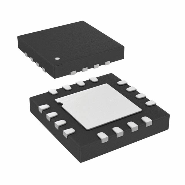
The ADL5565 is a high performance differential amplifier optimized for RF and IF applications. The amplifier offers low noise of 1.5 nV/√Hz and excellent distortion performance over a wide frequency range making it an ideal driver for high speed 8-bit to 16-bit analog-to-digital converters (ADCs). The ADL5565 provides three gain levels of 6 dB, 12 dB, and 15.5 dB through a pin strappable configuration. For the single-ended input configuration, the gains are reduced to 5.3 dB, 10.3 dB, and 13 dB. Using two external series resistors expands the gain flexibility of the amplifier and allows for any gain selection from 0 dB to 15.5 dB for a differential input and 0 dB to 13 dB for a single-ended input. The quiescent current of the ADL5565 is typically 70 mA, and when disabled, consumes less than 5 mA with −25 dB of inputto-output isolation at 100 MHz. The device is optimized for wideband, low distortion, and noise performance, giving it unprecedented performance for overall spurious-free dynamic range. These attributes, together with its adjustable gain capability, make this device the amplifier of choice for driving a wide variety of ADCs, mixers, pin diode attenuators, SAW filters, and multielement discrete devices. Fabricated on an Analog Devices, Inc., high speed SiGe process, the ADL5565 is supplied in a compact 3 mm × 3 mm, 16-lead LFCSP package and operates over the −40°C to +85°C temperature range.
Rev. 0
Information furnished by Analog Devices is believed to be accurate and reliable. However, no responsibility is assumed by Analog Devices for its use, nor for any infringements of patents or other rights of third parties that may result from its use. Specifications subject to change without notice. No license is granted by implication or otherwise under any patent or patent rights of Analog Devices. Trademarks and registered trademarks are the property of their respective owners.
One Technology Way, P.O. Box 9106, Norwood, MA 02062-9106, U.S.A. Tel: 781.329.4700 www.analog.com Fax: 781.461.3113 ©2011 Analog Devices, Inc. All rights reserved.
09959-001
RF
ADL5565
�ADL5565 TABLE OF CONTENTS
Features .............................................................................................. 1 Applications....................................................................................... 1 Functional Block Diagram .............................................................. 1 General Description ......................................................................... 1 Revision History ............................................................................... 2 Specifications..................................................................................... 3 3.3 V Specifications ...................................................................... 3 5 V Specifications ......................................................................... 6 Absolute Maximum Ratings............................................................ 9 ESD Caution.................................................................................. 9 Pin Configuration and Function Descriptions........................... 10 Typical Performance Characteristics ........................................... 11 Circuit Description......................................................................... 16 Basic Structure ............................................................................ 16 Applications Information .............................................................. 17 Basic Connections...................................................................... 17 Input and Output Interfacing ................................................... 18 Gain Adjustment and Interfacing ............................................ 19 ADC Interfacing ......................................................................... 20 Layout Considerations............................................................... 22 Soldering Information ............................................................... 23 Evaluation Board ........................................................................ 23 Outline Dimensions ....................................................................... 26 Ordering Guide .......................................................................... 26
REVISION HISTORY
10/11—Revision 0: Initial Version
Rev. 0 | Page 2 of 28
�ADL5565 SPECIFICATIONS
3.3 V SPECIFICATIONS
VS = 3.3 V, VCM = 1.65 V, RL = 200 Ω differential, AV = 6 dB, CL = 1 pF differential, f = 100 MHz, TA = 25°C; parameters specified ac-coupled differential input and differential output, unless otherwise noted. Table 1.
Parameter DYNAMIC PERFORMANCE −3 dB Bandwidth Test Conditions/Comments AV = 6 dB, VOUT ≤ 1.0 V p-p AV = 12 dB, VOUT ≤ 1.0 V p-p AV = 15.5 dB, VOUT ≤ 1.0 V p-p VOUT ≤ 1.0 V p-p VS ± 5% −40°C to +85°C Rise, AV = 15.5 dB, RL = 200 Ω, VOUT = 2 V step Fall, AV = 15.5 dB, RL = 200 Ω, VOUT = 2 V step 2 V step to 1% VIN = 4 V to 0 V step, VOUT ≤ ±10 mV Min Typ 6750 6500 6250 1000 ±1 1.9 0.35 11 11 2


 工商网监
湘ICP备2023018690号
工商网监
湘ICP备2023018690号