High IP3,
10 MHz to 6 GHz, Active Mixer
ADL5801
Data Sheet
FEATURES
FUNCTIONAL BLOCK DIAGRAM
VPLO GND NC IFON IFOP GND
24
23
22
21
20
18
VPRF
17
GND
16
RFIP
LOIN 4
15
RFIN
GND
5
14
GND
GND
6
13
VPDT
GND
1
GND
2
ADL5801
LOIP 3
V2I
BIAS
APPLICATIONS
Cellular base station receivers
Radio link downconverters
Broadband block conversion
Instrumentation
19
7
8
9
DET
10
11
12
VPLO GND ENBL VSET DETO GND
08079-001
Broadband upconverter/downconverter
Power conversion gain of 1.8 dB
Broadband RF, LO, and IF ports
SSB noise figure (NF) of 9.75 dB
Input IP3: 28.5 dBm
Input P1dB: 13.3 dBm
Typical LO drive: 0 dBm
Single-supply operation: 5 V at 130 mA
Adjustable bias for low power operation
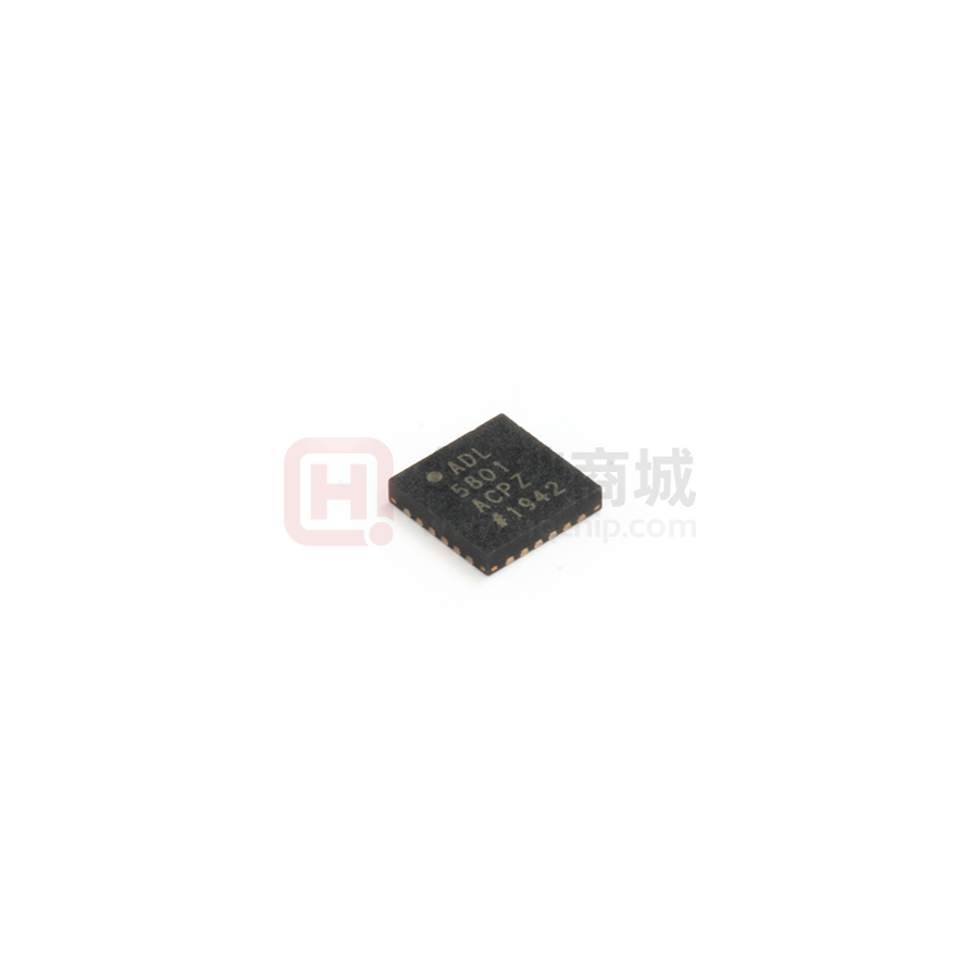
Exposed paddle, 4 mm × 4 mm, 24-lead LFCSP package
Figure 1.
GENERAL DESCRIPTION
The ADL5801 uses a high linearity, doubly balanced, active
mixer core with integrated LO buffer amplifier to provide high
dynamic range frequency conversion from 10 MHz to 6 GHz.
The mixer benefits from a proprietary linearization architecture
that provides enhanced input IP3 performance when subject to
high input levels. A bias adjust feature allows the input linearity,
SSB noise figure, and dc current to be optimized using a single
control pin. An optional input power detector is provided for
adaptive bias control. The high input linearity allows the device
to be used in demanding cellular applications where in-band
blocking signals may otherwise result in degradation in dynamic
performance. The adaptive bias feature allows the part to provide
high input IP3 performance when presented with large blocking
signals. When blockers are removed, the ADL5801 can automatically bias down to provide low noise figure and low power
consumption.
Rev. E
The balanced active mixer arrangement provides superb LO-toRF and LO-to-IF leakage, typically better than −40 dBm. The IF
outputs are designed to provide a typical voltage conversion
gain of 7.8 dB when loaded into a 200 Ω load. The broad
frequency range of the open-collector IF outputs allows the
ADL5801 to be applied as an upconverter for various transmit
applications.
The ADL5801 is fabricated using a SiGe high performance IC
process. The device is available in a compact 4 mm × 4 mm,
24-lead LFCSP package and operates over a −40°C to +85°C
temperature range. An evaluation board is also available.
Document Feedback
Information furnished by Analog Devices is believed to be accurate and reliable. However, no
responsibility is assumed by Analog Devices for its use, nor for any infringements of patents or other
rights of third parties that may result from its use. Specifications subject to change without notice. No
license is granted by implication or otherwise under any patent or patent rights of Analog Devices.
Trademarks and registered trademarks are the property of their respective owners.
One Technology Way, P.O. Box 9106, Norwood, MA 02062-9106, U.S.A.
Tel: 781.329.4700 ©2010–2014 Analog Devices, Inc. All rights reserved.
Technical Support
www.analog.com
�ADL5801
Data Sheet
TABLE OF CONTENTS
Features .............................................................................................. 1
Circuit Description......................................................................... 27
Applications ....................................................................................... 1
LO Amplifier and Splitter.......................................................... 27
Functional Block Diagram .............................................................. 1
RF Voltage-to-Current (V-to-I) Converter ............................. 27
General Description ......................................................................... 1
Mixer Core .................................................................................. 27
Revision History ............................................................................... 2
Mixer Output Load .................................................................... 27
Specifications..................................................................................... 3
RF Detector ................................................................................. 28
Absolute Maximum Ratings............................................................ 6
Bias Circuit .................................................................................. 28
ESD Caution .................................................................................. 6
Applications Information .............................................................. 31
Pin Configuration and Function Descriptions ............................. 7
Basic Connections ...................................................................... 31
Typical Performance Characteristics ............................................. 8
RF and LO Ports ......................................................................... 31
Downconverter Mode with a Broadband Balun ...................... 8
IF Port .......................................................................................... 32
Downconverter Mode with a Mini-Circuits® TC1-1-43M+
Input Balun .................................................................................. 12
Downconverting to Low Frequencies ...................................... 33
Downconverter Mode with a Johanson 3.5 GHz
Input Balun .................................................................................. 14
Single-Ended Drive of RF and LO Inputs ............................... 36
Downconverter Mode with a Johanson 5.7 GHz
Input Balun .................................................................................. 16
Upconverter Mode with a 900 MHz Output Match .............. 18
Broadband Operation ................................................................ 34
Evaluation Board ............................................................................ 38
Outline Dimensions ....................................................................... 40
Ordering Guide .......................................................................... 40
Upconverter Mode with a 2.1 GHz Output Match ................ 20
Spur Performance ....................................................................... 23
REVISION HISTORY
4/14—Rev. D to Rev. E
Changes to Figure 1 .......................................................................... 1
Changes to Table 1 ............................................................................ 4
Changes to Figure 87 and Deleted Table 4; Renumbered
Sequentially ..................................................................................... 27
Changes to RF Detector Section and Bias Circuit Section;
Added Table 4 and Table 5; Renumbered Sequentially, and
Added Figure 92, Figure 93, Figure 94, and Figure 95;
Renumbered Sequentially.............................................................. 29
3/14—Rev. C to Rev. D
Changes to Pin 9, Table 3 ................................................................. 7
8/13—Rev. B to Rev. C
Changes to Table 8 .......................................................................... 38
7/13—Rev. A to Rev. B
Added Disable Voltage and Enable Voltage; Table 1 .................... 3
Changes to Table 5 and Figure 96 ................................................. 31
Added Downconverting to Low Frequencies Section and
Figure 97; Renumbered Sequentially ........................................... 32
Added Broadband Operation Section and Figure 98 to
Figure 101 ........................................................................................ 33
Added Single-Ended Drive of RF and LO Inputs Section and
Figure 102 to Figure 105 ................................................................ 35
Updated Outline Dimensions ....................................................... 39
7/11—Rev. 0 to Rev. A
Changes to Specifications Section ...................................................3
Changes to Typical Performance Characteristics Section ...........8
Changes to Spur Performance Section ........................................ 23
Changes to RF Voltage-to-Current (V-to-I) Converter
Section.............................................................................................. 27
Changes to RF Detector Section................................................... 28
Changes to RF and LO Ports Section........................................... 30
2/10—Revision 0: Initial Version
Rev. E | Page 2 of 40
�Data Sheet
ADL5801
SPECIFICATIONS
VS = 5 V, TA = 25°C, fRF = 900 MHz, fLO = (fRF − 153 MHz), LO power = 0 dBm, Z0 1 = 50 Ω, VSET = 3.6 V, unless otherwise noted.
Table 1.
Parameter
RF INPUT INTERFACE
Return Loss
Input Impedance
RF Frequency Range
OUTPUT INTERFACE
Output Impedance
IF Frequency Range
DC Bias Voltage 2
LO INTERFACE
LO Power
Return Loss
Input Impedance
LO Frequency Range
POWER INTERFACE
Supply Voltage
Quiescent Current
Disable Current
Disable Voltage
Enable Voltage
Enable Time
Disable Time
DYNAMIC PERFORMANCE at fRF = 900 MHz/1900 MHz 3
Power Conversion Gain 4
Voltage Conversion Gain 5
SSB Noise Figure
SSB Noise Figure Under Blocking 6
Input Third-Order Intercept 7
Input Second-Order Intercept 8
Input 1 dB Compression Point
LO-to-IF Output Leakage
LO-to-RF Input Leakage
RF-to-IF Output Isolation
IF/2 Spurious 9
IF/3 Spurious9
Test Conditions
Min
Tunable to >20 dB over a limited bandwidth
Typ
LF
4.75
VS
0
15
50
10
4.75
fRF = 900 MHz
fRF = 1900 MHz
fRF = 900 MHz
fRF = 1900 MHz
fCENT = 900 MHz, VSET = 2.0 V
fCENT = 1900 MHz, VSET = 2.0 V
fCENT = 900 MHz
fCENT = 1900 MHz
fCENT = 900 MHz
fCENT = 1900 MHz
fCENT = 900 MHz
fCENT = 1900 MHz
fRF = 900 MHz
fRF = 1900 MHz
Unfiltered IF output
0 dBm input power, fRF = 900 MHz
0 dBm input power, fRF = 1900 MHz
0 dBm input power, fRF = 900 MHz
0 dBm input power, fRF = 1900 MHz
Rev. E | Page 3 of 40
6000
dB
Ω
MHz
600
5.25
Ω
MHz
V
230
−10
Resistor programmable
ENBL pin high to disable the device
ENBL pin high to disable the device
ENBL pin low to enable the device
Time from ENBL pin low to enable
Time from ENBL pin high to disable
Unit
12
50
10
Differential impedance, f = 200 MHz
Can be matched externally to 3000 MHz
Externally generated
Max
+10
6000
5
130
50
182
28
V
mA
mA
V
V
ns
ns
1.8
1.8
7.8
7.8
9.75
11.5
19.5
20
28.5
26.4
63
49.7
13.3
12.7
−27
−30
−35
−67.5
−53
−65.5
−72.6
dB
dB
dB
dB
dB
dB
dB
dB
dBm
dBm
dBm
dBm
dBm
dBm
dBm
dBm
dBc
dBc
dBc
dBc
dBc
2.5
0
5.25
200
dBm
dB
Ω
MHz
5
1.8
�ADL5801
Parameter
DYNAMIC PERFORMANCE at fRF = 2500 MHz 10
Power Conversion Gain 11
Voltage Conversion Gain5
SSB Noise Figure
Input Third-Order Intercept 12
Input Second-Order Intercept 13
Input 1 dB Compression Point
LO-to-IF Output Leakage
LO-to-RF Input Leakage
RF-to-IF Output Isolation
IF/2 Spurious9
IF/3 Spurious9
DYNAMIC PERFORMANCE at fRF = 3500 MHz 14
Power Conversion Gain 15
Voltage Conversion Gain5
SSB Noise Figure
Input Third-Order Intercept7
Input Second-Order Intercept8
Input 1 dB Compression Point
LO-to-IF Output Leakage
LO-to-RF Input Leakage
RF-to-IF Output Isolation
IF/2 Spurious9
IF/3 Spurious9
DYNAMIC PERFORMANCE at fRF = 5500 MHz 16
Power Conversion Gain 17
Voltage Conversion Gain5
SSB Noise Figure
Input Third-Order Intercept7
Input Second-Order Intercept 8
Input 1 dB Compression Point
LO-to-IF Output Leakage
LO-to-RF Input Leakage
RF-to-IF Output Isolation
IF/2 Spurious9
IF/3 Spurious9
DYNAMIC PERFORMANCE at fIF = 900 MHz 18
Power Conversion Gain 19
Voltage Conversion Gain5
SSB Noise Figure
Output Third-Order Intercept 20
Output Second-Order Intercept 21
Output 1 dB Compression Point
LO-to-IF Output Leakage
LO-to-RF Input Leakage
IF/2 Spurious9
IF/3 Spurious9
Data Sheet
Test Conditions
fCENT = 2500 MHz, VSET = 2.0 V
fCENT = 2500 MHz
fCENT = 2500 MHz
fCENT = 2500 MHz
Unfiltered IF output
0 dBm input power, fRF = 2600 MHz
0 dBm input power, fRF = 2600 MHz
fCENT = 3500 MHz, VSET = 3.6 V
fCENT = 3500 MHz, VSET = 3.6 V
fCENT = 3500 MHz, VSET = 3.6 V
Unfiltered IF output
0 dBm input power, fRF = 3800 MHz
0 dBm input power, fRF = 3800 MHz
fCENT = 5500 MHz, VSET = 3.6 V
fCENT = 5500 MHz, VSET = 3.6 V
fCENT = 5500 MHz, VSET = 3.6 V
Unfiltered IF output
0 dBm input power, fRF = 5800 MHz
0 dBm input power, fRF = 5800 MHz
fIF = 900 MHz, fRF = 250 MHz, VSET = 2.0 V
fCENT = 153 MHz, VSET = 3.6 V
fCENT = 153 MHz, VSET = 3.6 V
Unfiltered IF output
0 dBm input power, fRF = 140 MHz,
fIF = 806 MHz
0 dBm input power, fRF = 140 MHz,
fIF = 806 MHz
Rev. E | Page 4 of 40
Min
Typ
Max
Unit
−6.1
−0.1
10.6
25.5
45.3
13.8
−31.5
−31.2
−42.5
−50.6
−59.8
dB
dB
dB
dBm
dBm
dBm
dBm
dBm
dBc
dBc
dBc
−6.44
−0.44
15.8
26.5
42.3
12.5
−30.2
−29.4
−29.7
−47.1
−57.8
dB
dB
dB
dBm
dBm
dBm
dBm
dBm
dBc
dBc
dBc
−5.2
0.8
16.2
22.7
35.4
11.3
−42.6
−28.9
−46.7
−44
−47
dB
dB
dB
dBm
dBm
dBm
dBm
dBm
dBc
dBc
dBc
−6
0
10.6
30.6
68.7
11.1
−33.8
−33.4
−62.6
dB
dB
dB
dBm
dBm
dBm
dBm
dBm
dBc
−68.9
dBc
�Data Sheet
Parameter
DYNAMIC PERFORMANCE at fIF = 2140 MHz 22
Power Conversion Gain 23
Voltage Conversion Gain5
SSB Noise Figure
Output Third-Order Intercept 24
Output Second-Order Intercept 25
Output 1 dB Compression Point
LO-to-IF Output Leakage
LO-to-RF Input Leakage
IF/2 Spurious9
ADL5801
Test Conditions
fIF = 2140 MHz, fRF = 190 MHz, VSET = 2.0 V
fCENT = 170 MHz, VSET = 3.6 V
fCENT = 170 MHz, VSET = 3.6 V
Unfiltered IF output
0 dBm input power, fRF = 140 MHz,
fIF = 2210 MHz
Min
Typ
−7.25
−1.25
13.6
24
70
9.9
−23.8
−33.2
−51.5
Z0 is the characteristic impedance assumed for all measurements and the PCB.
Supply voltage must be applied from an external circuit through choke inductors
3
VS = 5 V, TA = 25°C, fRF = 900 MHz/1900 MHz, fLO = (fRF – 153 MHz), LO power = 0 dBm, Z01= 50 Ω, VSET = 3.8 V, unless otherwise noted.
4
Excluding 4:1 IF port transformer (TC4-1W+), RF and LO port transformers (TC1-1-13M+), and PCB loss.
5
ZSOURCE = 50 Ω, differential; ZLOAD = 200 Ω differential; ZSOURCE is the impedance of the source instrument; ZLOAD is the load impedance at the output.
6
fRF = fCENT, fBLOCKER = (fCENT − 5) MHz, fLO = (fCENT − 153) MHz, blocker level = 0 dBm.
7
fRF1 = (fCENT − 1) MHz, fRF2 = (fCENT) MHz, fLO = (fCENT – 153) MHz, each RF tone at −10 dBm.
8
fRF1 = (fCENT ) MHz, fRF2 = (fCENT + 100) MHz, fLO = (fCENT – 153) MHz, each RF tone at −10 dBm.
9
For details, see the Spur Performance section.
10
VS = 5 V, TA = 25°C, fRF = 2500 MHz, fLO = (fRF – 211 MHz), LO power = 0 dBm, Z01 = 50 Ω, VSET = 3.8 V, unless otherwise noted.
11
Including 4:1 IF port transformer (TC4-1W+), RF and LO port transformers (TC1-1-43M+ and TC1-1-13M+ respectively), and PCB loss.
12
fRF1 = (fCENT − 1) MHz, fRF2 = (fCENT) MHz, fLO = (fCENT – 211) MHz, each RF tone at −10 dBm.
13
fRF1 = (fCENT ) MHz, fRF2 = (fCENT + 100) MHz, fLO = (fCENT – 211) MHz, each RF tone at −10 dBm
14
VS = 5 V, TA = 25°C, fRF = 3500 MHz, fLO = (fRF – 153 MHz), LO power = 0 dBm, Z01 = 50 Ω, VSET = 3.6 V, unless otherwise noted.
15
Including 4:1 IF port transformer (TC4-1W+), RF and LO port transformers (3600BL14M050), and PCB loss.
16
VS = 5 V, TA = 25°C, fRF = 5500 MHz, fLO = (fRF – 153 MHz), LO power = 0 dBm, Z01 = 50 Ω, VSET = 3.6 V, unless otherwise noted.
17
Including 4:1 IF port transformer (TC4-1W+), RF and LO port transformers (5400BL14B050), and PCB loss.
18
VS = 5 V, TA = 25°C, fRF = 153 MHz, fLO = (fRF + 900 MHz), LO power = 0 dBm, Z01 = 50 Ω, VSET = 3.6 V, unless otherwise noted.
19
Including 4:1 IF port transformer (TC4-14+), RF and LO transformers (TC1-1-13M+), and PCB loss.
20
fRF1 = (fCENT − 1) MHz, fRF2 = (fCENT) MHz, fLO = (fCENT + 900 MHz), each RF tone at −10 dBm.
21
fRF1 = (fCENT ) MHz, fRF2 = (fCENT + 100) MHz, fLO = (fCENT + 900) MHz, each RF tone at −10 dBm.
22
VS = 5 V, TA = 25°C, fRF = 153MHz, fLO = (fRF + 2140 MHz), LO power = 0 dBm, Z01 = 50 Ω, VSET = 4 V, unless otherwise noted.
23
Including 4:1 IF port transformer (1850BL15B200), RF and LO port transformers (TC1-1-13M+), and PCB loss.
24
fRF1 = (fCENT − 1) MHz, fRF2 = (fCENT) MHz, fLO = (fCENT + 2140 MHz), each RF tone at −10 dBm.
25
fRF1 = (fCENT ) MHz, fRF2 = (fCENT + 100) MHz, fLO = (fCENT + 2140) MHz, each RF tone at −10 dBm.
1
2
Rev. E | Page 5 of 40
Max
Unit
dB
dB
dB
dBm
dBm
dBm
dBm
dBm
dBc
�ADL5801
Data Sheet
ABSOLUTE MAXIMUM RATINGS
Stresses above those listed under Absolute Maximum Ratings
may cause permanent damage to the device. This is a stress
rating only; functional operation of the device at these or any
other conditions above those indicated in the operational
section of this specification is not implied. Exposure to absolute
maximum rating conditions for extended periods may affect
device reliability.
Table 2.
Parameter
Supply Voltage, VPOS
VSET, ENBL
IFOP, IFON
RFIN Power
Internal Power Dissipation
θJA (Exposed Paddle Soldered Down)1
θJC (at Exposed Paddle)
Maximum Junction Temperature
Operating Temperature Range
Storage Temperature Range
1
Rating
5.5 V
5.5 V
5.5 V
20 dBm
1.2 W
26.5°C/W
8.7°C/W
150°C
−40°C to +85°C
−65°C to +150°C
ESD CAUTION
As measured on the evaluation board. For details, see the Evaluation Board
section.
Rev. E | Page 6 of 40
�Data Sheet
ADL5801
24
23
22
21
20
19
VPLO
GND
NC
IFON
IFOP
GND
PIN CONFIGURATION AND FUNCTION DESCRIPTIONS
1
2
3
4
5
6
PIN 1
INDICATOR
ADL5801
TOP VIEW
(Not to Scale)
18
17
16
15
14
13
VPRF
GND
RFIP
RFIN
GND
VPDT
NOTES
1. THERE IS AN EXPOSED PADDLE THAT
MUST BE SOLDERED TO GROUND.
2. NC = NO CONNECT.
08079-002
VPLO 7
GND 8
ENBL 9
VSET 10
DETO 11
GND 12
GND
GND
LOIP
LOIN
GND
GND
Figure 2. Pin Configuration
Table 3. Pin Function Descriptions
Pin No.
1, 2, 5, 6, 8, 12,
14, 17, 19, 23
3, 4
7, 24
9
Mnemonic
GND
Description
Device Common (DC Ground).
LOIP, LOIN
VPLO
ENBL
10
VSET
11
DETO
13
15, 16
VPDT
RFIN, RFIP
18
20, 21
VPRF
IFOP, IFON
22
NC
EPAD
Differential LO Input Terminal. Internally matched to 50 Ω. Must be ac-coupled.
Positive Supply Voltage for LO System.
Detector and Mixer Bias Enable. Pull the pin high to disable the internal detector and mixer bias circuit.
The device can be operated in this mode by setting the bias level using an external supply or connecting
a resistor from the VSET pin to the positive supply. See the Circuit Description section for more details.
Pull the pin low to enable the internal detector and mixer bias circuit.
Input IP3 Bias Adjustment. The voltage presented to the VSET pin sets the internal bias of the mixer core
and allows for adaptive control of the input IP3 and NF characteristics of the mixer core.
Detector Output. The DETO pin should be loaded with a capacitor to ground. The developed voltage is
proportional to the rms input level. When the DETO output voltage is connected to the VSET input pin,
the part auto biases and increases input IP3 performance when presented with large signal input levels.
Positive Supply Voltage for Detector.
Differential RF Input Terminal. Internally matched to 50 Ω differential input impedance. Must be
ac-coupled.
Positive Supply Voltage for RF Input System.
Differential IF Output Terminal. Bias must be applied through pull-up choke inductors or the center tap
of the IF transformer.
Not Connected.
The exposed paddle must be soldered to ground.
Rev. E | Page 7 of 40
�ADL5801
Data Sheet
TYPICAL PERFORMANCE CHARACTERISTICS
DOWNCONVERTER MODE WITH A BROADBAND BALUN
VS = 5 V, TA = 25°C, VSET = 3.8 V, IF = 153 MHz, as measured using a typical circuit schematic with low-side local oscillator (LO), unless
otherwise noted. Insertion loss of input and output baluns (TC1-1-13M+, TC4-1W+) is extracted from the gain measurement.
6
6
35
5
30
4
25
5
4
3
TA = +25°C
GAIN (dB)
GAIN (dB)
2
1
TA = +85°C
0
–1
–2
GAIN = 900MHz
GAIN = 1900MHz
INPUT IP3 = 900MHz
INPUT IP3 = 1900MHz
3
20
2
15
1
10
INPUT IP3 (dBm)
TA = –40°C
–3
2000
1500
2500
3000
RF FREQUENCY (MHz)
0
–15
5
–10
0
–5
10
5
08079-006
1000
08079-003
–4
500
15
LO LEVEL (dBm)
Figure 6. Power Conversion Gain and Input IP3 vs. LO Power
Figure 3. Power Conversion Gain vs. RF Frequency
100
4.0
90
3.5
MEAN = 1.87
SD = 0.03
80
3.0
FREQUENCY (%)
70
GAIN (dB)
2.5
900MHz
2.0
1.5
60
50
40
30
1900MHz
1.0
20
0.5
10
0.10
0.5
0.08
0
0.06
–0.5
0.04
3.5
4.0
4.5
0.02
5.0
VSET (V)
GAIN (dB)
1.0
SUPPLY CURRENT (A)
0.12
2.100
08079-007
TA = +25°C
2.0
TA = +85°C
1.5
1.0
0.5
08079-005
1.5
3.0
2.060
2.5
0.14
2.5
2.020
TA = –40°C
0.16
2.0
–1.0
2.0
1.980
3.0
0
4.7
4.8
4.9
5.0
5.1
5.2
SUPPLY (V)
Figure 8. Power Conversion Gain vs. Supply Voltage
Figure 5. Power Conversion Gain and Supply Current vs. VSET
Rev. E | Page 8 of 40
5.3
08079-008
2.5
GAIN (dB)
Figure 7. Power Conversion Gain Distribution
0.18
GAIN = 900MHz
GAIN = 1900MHz
IPOS = 900MHz
IPOS = 1900MHz
1.940
POWER CONVERSION GAIN (dB)
Figure 4. Power Conversion Gain vs. IF Frequency
3.0
1.900
IF FREQUENCY (MHz)
1.860
250
1.820
200
1.780
150
1.740
100
1.700
50
0
08079-004
0
0
�Data Sheet
ADL5801
70
35
TA = +25°C
60
TA = –40°C
TA = +25°C
TA = +85°C
TA = +85°C
15
40
30
10
20
5
10
0
500
1000
1500
2000
2500
3000
RF FREQUENCY (MHz)
0
500
1000
2000
1500
2500
3000
08079-012
20
250
08079-013
INPUT IP2 (dBm)
50
08079-009
INPUT IP3 (dBm)
25
5.0
08079-014
TA = –40°C
30
RF FREQUENCY (MHz)
Figure 9. Input IP3 vs. RF Frequency
Figure 12. Input IP2 vs. RF Frequency
40
80
70
35
900MHz
30
900MHz
INPUT IP2 (dBm)
INPUT IP3 (dBm)
60
1900MHz
25
20
50
1900MHz
40
30
20
15
10
0
100
50
0
150
200
250
IF FREQUENCY (MHz)
08079-010
10
0
100
50
150
200
IF FREQUENCY (MHz)
Figure 13. Input IP2 vs. IF Frequency
Figure 10. Input IP3 vs. IF Frequency
30
20
25
18
80
70
900MHz
15
14
10
12
INPUT IP2 (dBm)
16
NOISE FIGURE (dB)
20
50
1900MHz
40
30
20
INPUT IP3 = 900MHz
INPUT IP3 = 1900MHz
NF = 900MHz
NF = 1900MHz
5
10
10
0
8
0
2.0
2.5
3.0
3.5
4.0
4.5
VSET (V)
5.0
08079-011
INPUT IP3 (dBm)
60
Figure 11. Input IP3 and Noise Figure vs. VSET
2.0
2.5
3.0
3.5
4.0
VSET (V)
Figure 14. Input IP2 vs. VSET
Rev. E | Page 9 of 40
4.5
�ADL5801
Data Sheet
20
25
18
TA = +25°C
TA = +85°C
20
SSB NOISE FIGURE (dB)
INPUT P1dB (dBm)
16
14
12
TA = –40°C
10
8
6
15
1900MHz
10
900MHz
5
4
0
1000
2000
1500
2500
3000
RF FREQUENCY (MHz)
08079-015
0
500
0
100
300
200
400
500
600
700
IF FREQUENCY (MHz)
08079-018
2
Figure 18. SSB Noise Figure vs. IF Frequency (VSET = 2.0 V)
Figure 15. Input P1dB vs. RF Frequency
30
20
18
25
14
900MHz
12
1900MHz
SSB NOISE FIGURE (dB)
INPUT P1dB (dBm)
16
10
8
6
4
RF = 1846MHz, IF = 153 MHz
BLOCKER = 1841MHz
20
15
10
RF = 951MHz, IF = 153 MHz
BLOCKER = 946MHz
5
50
100
150
200
250
IF FREQUENCY (MHz)
0
–30
–15
–10
–5
0
5
Figure 19. SSB Noise Figure vs. Blocker Level (VSET = 2.0 V)
20
18
TA = +85°C
16
14
18
16
SSB NOISE FIGURE (dB)
TA = +25°C
12
10
TA = –40°C
8
6
14
10
900MHz
8
6
4
2
2
1000
1500
2000
2500
3000
RF FREQUENCY (MHz)
1900MHz
12
4
0
–15
08079-017
SSB NOISE FIGURE (dB)
–20
BLOCKER LEVEL (dBm)
Figure 16. Input P1dB vs. IF Frequency
0
500
–25
–10
–5
0
5
LO LEVEL (dBm)
10
Figure 20. SSB Noise Figure vs. LO Power (VSET = 2.0 V)
Figure 17. SSB Noise Figure vs. RF Frequency (VSET = 2.0 V)
Rev. E | Page 10 of 40
15
08079-020
0
08079-016
0
08079-019
2
�Data Sheet
ADL5801
0
–10
–15
5
LO-TO-IF LEAKAGE (dBm)
RF RETURN LOSS (dB)
–20
10
15
20
25
TA = –40°C
TA = +25°C
TA = +85°C
–25
–30
–35
–40
–45
–50
30
0
500
1000
1500
2000
2500
3000
RF FREQUENCY (MHz)
–60
500
08079-021
35
2500
3000
LO FREQUENCY (MHz)
Figure 21. RF Return Loss vs. RF Frequency
Figure 24. LO-to-IF Leakage vs. LO Frequency
0
–10
–15
5
LO-TO-RF LEAKAGE (dBm)
–20
LO RETURN LOSS (dB)
2000
1500
1000
08079-024
–55
10
15
20
25
TA = –40°C
TA = +25°C
TA = +85°C
–25
–30
–35
–40
–45
–50
30
500
1000
1500
2000
2500
3000
LO FREQUENCY (MHz)
–60
500
2500
3000
300
0
200
–2
100
RF-TO-IF OUTPUT ISOLATION (dBc)
2
CAPACITANCE (pF)
400
0
–4
–6
0
08079-023
RESISTANCE (Ω)
4
1000
2000
Figure 25. LO-to-RF Leakage vs. LO Frequency
500
100
1500
LO FREQUENCY (MHz)
Figure 22. LO Return Loss vs. LO Frequency
10
1000
3000
IF FREQUENCY (MHz)
Figure 23. IF Differential Output Impedance (R Parallel C Equivalent)
Rev. E | Page 11 of 40
–10
–20
–30
TA = +85°C
–40
TA = –40°C
TA = +25°C
–50
–60
500
1000
1500
2000
2500
RF FREQUENCY (MHz)
Figure 26. RF-to-IF Leakage vs. RF Frequency
3000
08079-026
0
08079-022
35
08079-025
–55
�ADL5801
Data Sheet
DOWNCONVERTER MODE WITH A MINI-CIRCUITS® TC1-1-43M+ INPUT BALUN
VS = 5 V, TA = 25°C, VSET = 3.8 V, IF = 211 MHz, as measured using a typical circuit schematic with low-side local oscillator (LO), unless
otherwise noted. Insertion loss of input and output baluns (TC1-1-43M+, TC4-1W+) is included in the gain measurement.
6
30
20
25
18
4
IIP3 2500MHz
INPUT IP3 (dBm)
3
GAIN (dB)
2
1
0
–1
20
16
15
14
10
12
NOISE FIGURE (dB)
5
NF 2500MHz
–2
10
5
–3
4.5
Figure 30. Input IP3 and Noise Figure vs. VSET
60
0.16
GAIN 2500M
50
0.10
IPOS 2500M
–1.0
0.08
–1.5
0.06
–2.0
INPUT IP2 (dBm)
0.12
–0.5
SUPPLY CURRENT (A)
0.14
0
40
30
20
0.04
10
–2.5
3.0
3.5
4.0
4.5
0
5.0
0
2000 2100 2200 2300 2400 2500 2600 2700 2800 2900 3000
08079-028
2.5
VSET (V)
RF FREQUENCY (MHz)
08079-031
0.02
–3.0
2.0
Figure 31. Input IP2 vs. RF Frequency
Figure 28. Power Conversion Gain and IPOS vs. VSET
30
80
29
70
28
60
INPUT IP2 (dBm)
27
26
25
24
50
40
30
23
20
22
20
2000 2100 2200 2300 2400 2500 2600 2700 2800 2900 3000
RF FREQUENCY (MHz)
Figure 29. Input IP3 vs. RF Frequency
0
2.0
2.5
3.0
3.5
4.0
VSET (V)
Figure 32. Input IP2 vs. VSET
Rev. E | Page 12 of 40
4.5
5.0
08079-032
10
21
08079-029
INPUT IP3 (dBm)
GAIN (dB)
4.0
VSET (V)
0.18
0.5
3.5
3.0
2.5
08079-030
2.0
Figure 27. Power Conversion Gain vs. RF Frequency
1.0
8
5.0
0
08079-027
–4
2000 2100 2200 2300 2400 2500 2600 2700 2800 2900 3000
RF FREQUENCY (MHz)
�ADL5801
–10
18
–15
16
–20
14
12
10
8
6
–25
–30
–35
–40
–45
4
–50
2
–55
0
2000 2100 2200 2300 2400 2500 2600 2700 2800 2900 3000
–60
2000 2100 2200 2300 2400 2500 2600 2700 2800 2900 3000
RF FREQUENCY (MHz)
LO FREQUENCY (MHz)
Figure 33. Input P1dB vs. RF Frequency
Figure 36. LO to RF Leakage vs. LO Frequency
25
–20
+85°C VSET 2V
+25°C VSET 2V
–40°C VSET 2V
15
10
0
2000 2100 2200 2300 2400 2500 2600 2700 2800 2900 3000
RF FREQUENCY (MHz)
08079-034
5
Figure 34. Noise Figure vs. RF Frequency
–15
–25
–30
–35
–40
–45
–50
–55
08079-035
LO TO IF LEAKAGE (dBm)
–20
LO FREQUENCY (MHz)
–40
–50
–60
–70
–80
2000 2100 2200 2300 2400 2500 2600 2700 2800 2900 3000
RF FREQUENCY (MHz)
Figure 37. RF to IF Output Isolation vs. RF Frequency
–10
–60
2000 2100 2200 2300 2400 2500 2600 2700 2800 2900 3000
–30
Figure 35. LO to IF Leakage vs. LO Frequency
Rev. E | Page 13 of 40
08079-037
+85°C VSET 3.6V
+25°C VSET 3.6V
–40°C VSET 3.6V
RF TO IF OUTPUT ISOLATION (dBc)
NOISE FIGURE (dB)
20
08079-036
LO TO RF LEAKAGE (dBm)
20
08079-033
INPUT P1dB (dBm)
Data Sheet
�ADL5801
Data Sheet
DOWNCONVERTER MODE WITH A JOHANSON 3.5 GHZ INPUT BALUN
VS = 5 V, TA = 25°C, VSET = 3.6 V, IF = 153 MHz, as measured using a typical circuit schematic with low-side local oscillator (LO), unless
otherwise noted. Insertion loss of input and output baluns (3600BL14M050, TC4-1W+) is included in the gain measurement.
5
4
28
30
6
–40°C
+25°C
+85°C
25
2
1
0
18
15
10
–1
–2
IIP3, –40°C
IIP3, +25°C
IIP3, +85°C
NF, –40°C
NF, +25°C
NF, +85°C
5
–3
RF FREQUENCY (MHz)
0
2.0
08079-038
–4
3000 3100 3200 3300 3400 3500 3600 3700 3800 3900 4000
8
2.5
3.0
3.5
4.0
4.5
Figure 41. Input IP3 and Noise Figure vs. VSET
0.20
50
0.18
0
0.08
GAIN –40°C
GAIN +25°C
GAIN +85°C
IPOS –40°C
IPOS +25°C
IPOS +85°C
–12
2.0
2.5
40
35
30
0.04
25
0.02
3.0
3.5
4.0
4.5
0
5.0
20
3000 3100 3200 3300 3400 3500 3600 3700 3800 3900 4000
VSET (V)
RF FREQUENCY (MHz)
Figure 42. Input IP2 vs. RF Frequency
Figure 39. Power Conversion Gain and IPOS vs. VSET
80
30
25
08079-042
–10
0.06
08079-039
–8
INPUT IP2 (dBm)
0.10
–6
SUPPLY CURRENT (A)
0.12
–4
–40°C
+25°C
+85°C
70
+85°C
+25°C
–40°C
60
INPUT IP2 (dBm)
20
15
10
50
40
30
20
5
0
3000 3100 3200 3300 3400 3500 3600 3700 3800 3900 4000
RF FREQUENCY (MHz)
Figure 40. Input IP3 vs. RF Frequency
0
2.0
2.5
3.0
3.5
4.0
VSET (V)
Figure 43. Input IP2 vs. VSET
Rev. E | Page 14 of 40
4.5
5.0
08079-043
10
08079-040
INPUT IP3 (dBm)
GAIN (dB)
0.14
+85°C
+25°C
–40°C
45
0.16
–2
5.0
VSET (V)
Figure 38. Power Conversion Gain vs. RF Frequency
2
13
08079-041
INPUT IP3 (dBm)
GAIN (dB)
20
NOISE FIGURE (dB)
23
3
�Data Sheet
ADL5801
–10
20
–15
–20
12
10
8
–25
–30
–35
–40
–45
–50
2
–55
0
3000 3100 3200 3300 3400 3500 3600 3700 3800 3900 4000
–60
3000 3100 3200 3300 3400 3500 3600 3700 3800 3900 4000
RF FREQUENCY (MHz)
08079-044
4
LO FREQUENCY (MHz)
Figure 47. LO to RF Leakage vs. LO Frequency
Figure 44. Input P1dB vs. RF Frequency
–20
25
+25°C, 3.6V
–40°C, 3.6V
RF TO IF OUTPUT ISOLATION (dBc)
+85°C, 3.6V
NOISE FIGURE (dB)
20
15
+85°C, 2.0V
+25°C, 2.0V
–40°C, 2.0V
10
0
3000 3100 3200 3300 3400 3500 3600 3700 3800 3900 4000
RF FREQUENCY (MHz)
08079-045
5
–10
–15
+85°C
+25°C
–40°C
–25
–30
–35
–40
–45
–50
LO FREQUENCY (MHz)
08079-046
–55
–60
3000 3100 3200 3300 3400 3500 3600 3700 3800 3900 4000
–30
–40
+85°C
+25°C
–40°C
–50
–60
–70
–80
3000 3100 3200 3300 3400 3500 3600 3700 3800 3900 4000
RF FREQUENCY (MHz)
Figure 48. RF to IF Output Isolation vs. RF Frequency
Figure 45. Noise Figure vs. RF Frequency
–20
08079-047
14
6
LO TO IF LEAKAGE (dBm)
+85°C
+25°C
–40°C
Figure 46. LO to IF Leakage vs. LO Frequency
Rev. E | Page 15 of 40
08079-048
INPUT P1dB (dBm)
16
+85°C
+25°C
–40°C
LO TO RF LEAKAGE (dBm)
18
�ADL5801
Data Sheet
DOWNCONVERTER MODE WITH A JOHANSON 5.7 GHZ INPUT BALUN
VS = 5 V, TA = 25°C, VSET = 3.6 V, IF = 153 MHz, as measured using a typical circuit schematic with low-side local oscillator (LO), unless
otherwise noted. Insertion loss of input and output baluns (5400BL14B050, TC4-1W+) is included in the gain measurement.
30
20
3
1
0
15
20
10
15
–1
IIP3, –40°C
IIP3, +25°C
IIP3, +85°C
NF, –40°C
NF, +25°C
NF, +85°C
5
–2
–3
RF FREQUENCY (MHz)
0
2.0
08079-049
–4
5000 5100 5200 5300 5400 5500 5600 5700 5800 5900 6000
70
0
0.18
65
–2
0.16
60
–6
0.10
–8
0.08
0.06
GAIN –40°C
GAIN +25°C
GAIN +85°C
IPOS –40°C
IPOS +25°C
IPOS +85°C
–14
–16
2.0
2.5
3.0
3.5
4.0
4.5
4.5
5
5.0
45
40
35
30
0.02
25
0
5.0
+85°C
+25°C
–40°C
50
0.04
VSET (V)
20
5000 5100 5200 5300 5400 5500 5600 5700 5800 5900 6000
RF FREQUENCY (MHz)
Figure 53. Input IP2 vs. RF Frequency
Figure 50. Power Conversion Gain and IPOS vs VSET
30
4.0
55
08079-050
GAIN (dB)
0.12
INPUT IP2 (dBm)
0.14
SUPPLY CURRENT (A)
0.20
–12
3.5
Figure 52. Input IP3 and Noise Figure vs. VSET
2
–10
3.0
10
VSET (V)
Figure 49. Power Conversion Gain vs. RF Frequency
–4
2.5
NOISE FIGURE (dB)
25
INPUT IP3 (dBm)
GAIN (dB)
2
08079-052
4
–40°C
+25°C
+85°C
08079-053
5
35
25
6
80
–40°C
+25°C
+85°C
70
25
+85°C
+25°C
–40°C
INPUT IP2 (dBm)
20
15
50
40
30
10
20
5
0
5000 5100 5200 5300 5400 5500 5600 5700 5800 5900 6000
RF FREQUENCY (MHz)
0
2.0
2.5
3.0
3.5
4.0
VSET (V)
Figure 54. Input IP2 vs. VSET
Figure 51. Input IP3 vs. RF Frequency
Rev. E | Page 16 of 40
4.5
5.0
08079-054
10
08079-051
INPUT IP3 (dBm)
60
�Data Sheet
ADL5801
20
–15
–20
14
12
10
8
6
–25
–30
–35
–40
–45
–50
2
–55
0
5000 5100 5200 5300 5400 5500 5600 5700 5800 5900 6000
–60
5000 5100 5200 5300 5400 5500 5600 5700 5800 5900 6000
RF FREQUENCY (MHz)
08079-055
4
LO FREQUENCY (MHz)
Figure 55. Input P1dB vs. RF Frequency
Figure 58. LO to RF Leakage vs. LO Frequency
25
–20
+25°C, 3.6V
–40°C, 3.6V
RF TO IF OUTPUT ISOLATION (dBc)
+85°C, 3.6V
NOISE FIGURE (dB)
20
15
+85°C, 2.0V
+25°C, 2.0V
–40°C, 2.0V
10
0
5000 5100 5200 5300 5400 5500 5600 5700 5800 5900 6000
RF FREQUENCY (MHz)
08079-056
5
Figure 56. Noise Figure vs. RF Frequency, VSET = 3.6 V
–15
–25
–30
–35
–40
–45
–50
–55
LO FREQUENCY (MHz)
08079-057
LO TO IF LEAKAGE (dBm)
+85°C
+25°C
–40°C
–60
5000 5100 5200 5300 5400 5500 5600 5700 5800 5900 6000
–30
+85°C
+25°C
–40°C
–40
–50
–60
–70
–80
5000 5100 5200 5300 5400 5500 5600 5700 5800 5900 6000
RF FREQUENCY (MHz)
Figure 59. RF to IF Output Isolation vs. RF Frequency
–10
–20
08079-058
LO TO RF LEAKAGE (dBm)
INPUT P1dB (dBm)
16
+85°C
+25°C
–40°C
Figure 57. LO to IF Leakage vs. LO Frequency
Rev. E | Page 17 of 40
08079-059
18
–10
+85°C
+25°C
–40°C
�ADL5801
Data Sheet
UPCONVERTER MODE WITH A 900 MHZ OUTPUT MATCH
VS = 5 V, TA = 25°C, VSET = 3.6 V, RF = 153 MHz, as measured using a typical circuit schematic with low-side local oscillator (LO),
unless otherwise noted. Insertion loss of input and output baluns (TC1-1-13M+, TC4-14) is included in the gain measurement.
2
35
1
+85°C
+25°C
–40°C
0
30
OUTPUT IP3 (dBm)
GAIN (dB)
–1
–2
–3
–4
–5
25
20
15
OUTPUT IP3, –40°C
OUTPUT IP3, +25°C
OUTPUT IP3, +85°C
10
–6
5
300
400
500
600
700
800
900
1000 1100 1200 1300
IF FREQUENCY (MHz)
0
2.0
08079-077
–8
2.5
5.0
0.16
75
0.14
0.12
0.2
0.1
0
0.08
–0.2
0.06
–0.4
OUTPUT IP2 (dBm)
GAIN (dB)
0.4
4.5
80
SUPPLY CURRENT (A)
0.6
4.0
Figure 63. Output IP3 vs. VSET
0.18
GAIN –40°C
GAIN +25°C
GAIN +85°C
IPOS –40°C
IPOS +25°C
IPOS +85°C
0.8
3.5
VSET (V)
Figure 60. Power Conversion Gain vs. IF Frequency
1.0
3.0
08079-080
–7
+85°C
+25°C
–40°C
70
65
60
0.04
–0.6
55
2.5
3.5
3.0
4.0
4.5
0
5.0
50
300
400
500
VSET (V)
800
900
1000 1100 1200 1300
Figure 64. Output IP2 vs. IF Frequency
35
80
30
75
70
OUTPUT IP2 (dBm)
25
20
+85°C
+25°C
–40°C
15
10
65
+85°C
+25°C
–40°C
60
55
50
5
45
400
500
600
700
800
900
1000 1100 1200 1300
IF FREQUENCY (MHz)
08079-079
OUTPUT IP3 (dBm)
700
IF FREQUENCY (MHz)
Figure 61. Power Conversion Gain and IPOS vs. VSET
0
300
600
Figure 62. Output IP3 vs. IF Frequency
40
2.0
2.5
3.0
3.5
4.0
VSET (V)
Figure 65. Output IP2 vs. VSET
Rev. E | Page 18 of 40
4.5
5.0
08079-082
–1.0
2.0
08079-081
0.02
–0.8
�Data Sheet
ADL5801
–10
12
–15
–20
LO TO IF LEAKAGE (dBm)
OUTPUT P1dB (dBm)
10
8
6
+85°C
+25°C
–40°C
4
–25
+85°C
+25°C
–40°C
–30
–35
–40
–45
–50
2
400
500
600
700
800
900
1000
1100
IF FREQUENCY (MHz)
–60
453
08079-083
0
300
553
653
753
853
953
1053 1153 1253 1353 1453
LO FREQUENCY (MHz)
08079-085
–55
Figure 68. LO to IF Leakage vs. LO Frequency
Figure 66. Output P1dB vs. IF Frequency
–10
16
–15
14
LO TO RF LEAKAGE (dBm)
–20
10
8
6
NF
NF
NF
4
VSET = 3.6V, –40°C
VSET = 3.6V, +25°C
VSET = 3.6V, +85°C
NF
NF
NF
VSET = 2.0V, –40°C
VSET = 2.0V, +25°C
VSET = 2.0V, +85°C
–25
–30
–35
–40
+85°C
+25°C
–40°C
–45
–50
2
750
800
850
900
950
IF FREQUENCY (MHz)
1000
–60
453
553
653
753
853
953
1053 1153 1253 1353 1453
LO FREQUENCY (MHz)
Figure 69. LO to RF Leakage vs. LO Frequency
Figure 67. Noise Figure vs. IF Frequency, FLO = 650 MHz
Rev. E | Page 19 of 40
08079-086
–55
0
700
08079-084
NOISE FIGURE (dB)
12
�ADL5801
Data Sheet
UPCONVERTER MODE WITH A 2.1 GHZ OUTPUT MATCH
VS = 5 V, TA = 25°C, VSET = 4 V, RF = 170 MHz, as measured using a typical circuit schematic with low-side local oscillator (LO), unless
otherwise noted. Insertion loss of input and output baluns (TC1-1-13M+, 1850BL15B200) is included in the gain measurement.
4
35
3
30
2
OUTPUT IP3 (dBm)
0
–1
–2
–3
170
190
210
230
250
270
290
RF FREQUENCY (MHz)
0
110
0.16
75
0.08
–3.0
2.0
0.06
250
270
290
+85°C
+25°C
–40°C
70
65
60
55
0.02
3.0
2.5
230
0.04
3.5
4.0
0
5.0
4.5
50
1900
08079-062
–2.5
VSET (V)
2000
2100
2200
2300
2400
2500
2600
2700
IF FREQUENCY (MHz)
Figure 74. Output IP2 vs. IF Frequency
Figure 71. Power Conversion Gain and IPOS vs. VSET
80
35
75
30
+85°C
+25°C
–40°C
70
OUTPUT IP2 (dBm)
25
20
15
10
65
60
55
50
OUTPUT IP3 –40°C
OUTPUT IP3 +25°C
OUTPUT IP3 +85°C
45
0
2.0
2.5
3.0
3.5
VSET (V)
4.0
4.5
5.0
40
2.0
2.5
3.0
3.5
4.0
VSET (V)
Figure 75. Output IP2 vs. VSET
Figure 72. Output IP3 vs. VSET
Rev. E | Page 20 of 40
4.5
5.0
08079-070
5
08079-067
OUTPUT IP3 (dBm)
GAIN (dB)
0.10
–1.5
OUTPUT IP2 (dBm)
0.12
SUPPLY CURRENT (A)
0.14
GAIN –40°C
GAIN +25°C
GAIN +85°C
IPOS –40°C
IPOS +25°C
IPOS +85°C
210
80
–0.5
–2.0
190
Figure 73. Output IP3 vs. RF Frequency
0.18
–1.0
170
RF FREQUENCY (MHz)
Figure 70. Power Conversion Gain vs. RF Frequency
0
150
130
08079-065
150
08079-060
130
–40°C
+25°C
+85°C
15
5
–5
–6
110
20
10
–40°C
+25°C
+85°C
–4
25
08079-069
GAIN (dB)
1
�Data Sheet
ADL5801
–10
12
–15
–20
LO TO RF LEAKAGE (dBm)
OUTPUT P1DB (dBm)
10
+85°C
+25°C
–40°C
8
6
4
+85°C
+25°C
–40°C
–25
–30
–35
–40
–45
–50
2
2100
2200
2300
2400
2600
2500
2700
IF FREQUENCY (MHz)
–60
2070
08079-072
2000
2170
2270
2370
2470
2570
2670
2770
08079-075
–55
0
1900
2870
LO FREQUENCY (MHz)
Figure 76. Output P1dB vs. IF Frequency
Figure 79. LO to RF Leakage vs. LO Frequency
–65
25
RF TO IF OUTPUT ISOLATION (dBc)
–66
NOISE FIGURE (dB)
20
15
10
NF
NF
NF
5
VSET = 3.6V, –40°C
VSET = 3.6V, +25°C
VSET = 3.6V, +85°C
NF
NF
NF
VSET = 2.0V, –40°C
VSET = 2.0V, +25°C
VSET = 2.0V, +85°C
+85°C
+25°C
–40°C
–67
–68
–69
–70
–71
–72
–73
2150
2200
2250
2300
IF FREQUENCY (MHz)
–75
110
–15
1
–20
0
–25
–1
GAIN (dB)
+85°C
+25°C
–40°C
–40
–6
–55
–7
2370
2470
2570
2670
2770
LO FREQUENCY (MHz)
2870
230
250
270
290
–40°C
+25°C
+85°C
–4
–50
2270
210
–3
–5
2170
190
–2
–45
08079-074
LO TO IF LEAKAGE (dBm)
2
–60
2070
170
Figure 80. RF to IF Output Isolation vs. RF Frequency
–10
–35
150
RF FREQUENCY (MHz)
Figure 77. Noise Figure vs. IF Frequency, FLO = 1950 MHz
–30
130
–8
1900
2000
2100
2200
2300
2400
2500
2600
IF FREQUENCY (MHz)
Figure 81. Power Conversion Gain vs. IF Frequency
Figure 78. LO to IF Leakage vs. LO Frequency
Rev. E | Page 21 of 40
2700
08079-061
2100
08079-073
2050
08079-076
–74
0
2000
�ADL5801
Data Sheet
5
40
80
4
35
78
0
15
–1
OUTPUT IP3 (dBm)
20
OUTPUT IP3 –40°C
OUTPUT IP3 +25°C
OUTPUT IP3 +85°C
GAIN –40°C
GAIN +25°C
GAIN +85°C
–3
–4
–10
–8
–6
–4
0
–2
2
4
6
8
74
72
5
68
0
66
110
10
LO POWER (dBm)
150
170
190
210
230
250
270
290
270
290
Figure 85. Output IP2 vs. RF Frequency
20
0
18
–40°C
+25°C
+85°C
16
OUTPUT P1dB (dBm)
–0.4
GAIN (dB)
130
RF FREQUENCY (MHz)
Figure 82. Power Conversion Gain and Output IP3 vs. LO Power
–0.2
–40°C
+25°C
+85°C
76
70
10
–2
08079-063
GAIN (dB)
25
1
OUTPUT IP2 (dBm)
30
2
08079-068
3
–0.6
–0.8
–1.0
+85°C
+25°C
–40°C
14
12
10
8
6
4
–1.2
4.90
4.95
5.00
5.05
5.10
5.15
5.20
5.25
SUPPLY (V)
Figure 83. Power Conversion Gain vs. Supply
20
15
10
5
2000
2100
2200
2300
2400
2500
IF FREQUENCY (MHz)
2600
2700
08079-066
OUTPUT IP3 (dBm)
–40°C
+25°C
+85°C
25
0
1900
130
150
170
190
210
230
250
RF FREQUENCY (MHz)
Figure 86. Output P1dB vs. RF Frequency
35
30
0
110
Figure 84. Output IP3 vs. IF Frequency
Rev. E | Page 22 of 40
08079-071
4.85
4.80
08079-064
–1.4
4.75
2
�Data Sheet
ADL5801
SPUR PERFORMANCE
All spur tables are (N × fRF) − (M × fLO) and were measured using the standard evaluation board (see the Evaluation Board section). Mixer
spurious products are measured in decibels relative to the carrier (dBc) from the IF output power level. Data was measured for frequencies
less than 6 GHz only. The typical noise floor of the measurement system is −100 dBm.
900 MHz Downconvert Performance
VS = 5 V, VSET = 3.8 V, TA = 25°C, RF power = 0 dBm, LO power = 0 dBm, fRF = 900 MHz, fLO = 703 MHz, Z0 = 50 Ω.
0
N
0
1
2
3
4
5
6
7
8
9
10
11
12
13
14
15
−48.8
−35.9
−68.8
−47.5
−95.6
−85.7
1
−33.1
0.0
−74.9
−64.8
−80.7
−74.7
−96.4
≤−100
2
−23.3
−51.5
−67.5
−94.3
−78.0
−89.8
−83.1
≤−100
≤−100
3
−45.8
−19.0
−66.1
−65.9
−78.4
−70.7
−98.5
−95.9
≤−100
≤−100
4
−23.6
−65.1
−73.5
−86.3
−95.1
−84.8
−83.3
≤−100
−99.0
≤−100
5
−45.9
−29.6
−80.5
−70.2
−73.5
−90.7
−96.7
−97.2
−99.8
≤−100
≤−100
6
−30.7
−78.0
−65.0
−76.3
−89.4
−86.7
≤−100
−83.1
−86.0
−90.9
≤−100
≤−100
M
7
−55.4
−50.3
−89.8
−70.6
−87.3
−86.4
−89.4
−84.1
≤−100
−88.4
≤−100
≤−100
≤−100
8
−41.5
−74.4
−71.3
−74.5
≤−100
−83.1
−99.6
≤−100
≤−100
−83.5
−97.9
−92.6
≤−100
9
−57.7
−88.5
−81.4
−92.7
−73.7
−96.1
≤−100
≤−100
−87.6
−95.5
−87.4
≤−100
≤−100
10
11
12
13
14
−86.8
≤−100
−99.5
−78.7
−96.1
−99.7
≤−100
≤−100
−99.0
−88.2
≤−100
≤−100
≤−100
−98.8
−99.6
−99.4
−80.7
−95.4
−87.9
≤−100
≤−100
≤−100
−92.3
≤−100
−95.1
≤−100
≤−100
≤−100
≤−100
−91.1
−95.5
−88.8
≤−100
≤−100
≤−100
−99.3
≤−100
−96.5
≤−100
≤−100
≤−100
≤−100
≤−100
−85.7
≤−100
≤−100
≤−100
≤−100
≤−100
−90.4
≤−100
≤−100
≤−100
≤−100
≤−100
≤−100
≤−100
≤−100
≤−100
≤−100
≤−100
≤−100
≤−100
13
14
1900 MHz Downconvert Performance
VS = 5 V, VSET = 3.8 V, TA = 25°C, RF power = 0 dBm, LO power = 0 dBm, fRF = 1900 MHz, fLO = 1703 MHz, Z0 = 50 Ω.
M
0
N
0
1
2
3
4
5
6
7
8
9
10
11
12
13
14
15
−40.4
−38.4
≤−100
1
−31.4
0.0
−66.0
−66.2
≤−100
2
−17.1
−53.6
−52.9
−73.2
−89.4
3
−51.4
−38.5
−68.1
−72.6
−86.4
−83.7
4
−71.0
−64.2
−79.9
−94.6
−66.2
≤−100
5
−86.8
−65.2
−87.4
−79.3
−86.4
≤−100
6
−92.8
−81.5
−89.0
≤−100
−92.4
≤−100
7
≤−100
−75.2
−99.0
−92.7
≤−100
≤−100
Rev. E | Page 23 of 40
8
9
≤−100
−87.7
≤−100
−97.5
≤−100
≤−100
≤−100
≤−100
−98.4
≤−100
≤−100
−97.2
≤−100
10
≤−100
≤−100
−95.4
≤−100
−95.6
≤−100
≤−100
11
12
≤−100
≤−100
≤−100
≤−100
≤−100
≤−100
≤−100
≤−100
≤−100
≤−100
≤−100
≤−100
≤−100
≤−100
≤−100
≤−100
≤−100
≤−100
≤−100
≤−100
≤−100
≤−100
≤−100
≤−100
≤−100
�ADL5801
Data Sheet
2600 MHz Downconvert Performance
VS = 5 V, VSET = 3.8 V, TA = 25°C, RF power = 0 dBm, LO power = 0 dBm, fRF = 2600 MHz, fLO = 2350 MHz, Z0 = 50 Ω.
M
0
N
0
1
2
3
4
5
6
7
8
9
10
11
12
13
14
15
−40.3
−71.7
1
−31.5
0.0
−73.6
−83.9
2
−30.3
−55.8
−50.6
−66.5
−94.7
3
4
−33.8
−70.4
−59.8
−77.6
−91.4
−64.8
−71.3
−92.6
−71.1
5
−84.7
−83.8
−89.7
−83.1
6
−90.6
−98.2
−90.3


 工商网监
湘ICP备2023018690号
工商网监
湘ICP备2023018690号
