200 MHz to 6 GHz
35 dB TruPwr™ Detector
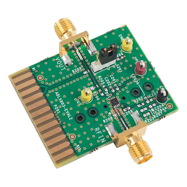
ADL5903
Data Sheet
FUNCTIONAL BLOCK DIAGRAM
Accurate rms-to-dc conversion from 200 MHz to 6 GHz
Measurement dynamic range of 35 dB
Ripple-free transfer function
Single-ended input, 50 Ω source compatible
No external matching required
Waveform and modulation independent, such as
GSM/CDMA/W-CDMA/TD-SCDMA/LTE
Linear in decibels output, scaled 35.5 mV/dB at 900 MHz
Excellent temperature stability
Operates from 3.0 V to 5.0 V from −55°C to +125°C
Low power consumption: 3 mA at 3.0 V to 5.0 V supply
8-lead, 2 mm × 2 mm LFCSP package
VPOS
CREG
5
4
ADL5903
ENBL 6
INTERNAL
FILTERING
1kΩ
630pF
3 CRMS
4pF
RFIN 1
100Ω
RMS CORE
7 VRMS
BUFFER
2
8
GND
NIC
EP
11769-001
FEATURES
Figure 1.
APPLICATIONS
Power amplifier linearization/control loops
Transmitter power controls
Transmitter signal strength indication (TSSI)
RF instrumentation
Wireless repeaters
GENERAL DESCRIPTION
The ADL5903 is a true rms responding power detector that has
a 35 dB measurement range. It features low power consumption
and an intrinsically ripple-free error transfer function.
The ADL5903 provides a solution in a variety of high frequency
systems requiring an accurate measurement of signal power.
Requiring only a single supply of 3.0 V to 5.0 V and a few
capacitors, it is easy to use and capable of being driven singleended or with a balun for differential input drive. An on-chip
matching network provides good return loss over the specified
frequency range of the device. The ADL5903 can operate from
200 MHz to 6 GHz and can accept inputs from −30 dBm to
+20 dBm.
Rev. B
The ADL5903 can be used to determine the true power of a
high frequency signal with a complex modulation envelope
including large crest factor signals such as GSM, CDMA,
W-CDMA, TD-SCDMA, and LTE modulated signals. The
output is then proportional to the logarithm of the rms value
of the input. In other words, the reading is presented directly
in decibels and is scaled about 35.5 mV/dB at 900 MHz.
The ADL5903 has low power consumption when operational
and a disable mode that further reduces the power consumption.
Power consumption is less than 100 µA when the ADL5903
enters power-down mode through a logic low at Pin ENBL.
The ADL5903 is supplied in a 2 mm × 2 mm, 8-lead LFCSP for
operation over the wide temperature range of −55°C to +125°C.
Document Feedback
Information furnished by Analog Devices is believed to be accurate and reliable. However, no
responsibility is assumed by Analog Devices for its use, nor for any infringements of patents or other
rights of third parties that may result from its use. Specifications subject to change without notice. No
license is granted by implication or otherwise under any patent or patent rights of Analog Devices.
Trademarks and registered trademarks are the property of their respective owners.
One Technology Way, P.O. Box 9106, Norwood, MA 02062-9106, U.S.A.
Tel: 781.329.4700 ©2013–2015 Analog Devices, Inc. All rights reserved.
Technical Support
www.analog.com
�ADL5903
Data Sheet
TABLE OF CONTENTS
Features .............................................................................................. 1
Measurement Setups ...................................................................... 14
Applications ....................................................................................... 1
Theory of Operation ...................................................................... 15
Functional Block Diagram .............................................................. 1
RF Input Interface ...................................................................... 15
General Description ......................................................................... 1
Basic Connections ...................................................................... 15
Revision History ............................................................................... 2
Choosing a Value for CRMS......................................................... 16
Specifications..................................................................................... 3
Device Calibration and Error Calculation .............................. 17
Absolute Maximum Ratings ............................................................ 6
Evaluation Board Schematic and Configuration Options ........ 19
ESD Caution .................................................................................. 6
Outline Dimensions ....................................................................... 20
Pin Configuration and Function Descriptions ............................. 7
Ordering Guide .......................................................................... 20
Typical Performance Characteristics ............................................. 8
REVISION HISTORY
5/15—Rev. A to Rev. B
Changes to Figure 49 ...................................................................... 19
2/15—Rev. 0 to Rev. A
Added ADL5903ACPZN Operating Temperature Range of
−40°C to +85°C; Table 2 .................................................................. 6
Changes to Ordering Guide .......................................................... 20
10/13—Revision 0: Initial Version
Rev. B | Page 2 of 20
�Data Sheet
ADL5903
SPECIFICATIONS
VPOS = 5.0 V, TA = 25°C, ZO = 50 Ω, Capacitor CRMS = 10 nF, unless otherwise noted.
Table 1.
Parameter
OVERALL FUNCTION
Frequency Range
RF INPUT INTERFACE
Nominal Input Impedance1
OUTPUT INTERFACE
DC Output Resistance
Rise Time
Fall Time
f = 300 MHz
±1.0 dB Dynamic Range
Maximum Input Level, ±1.0 dB
Minimum Input Level, ±1.0 dB
Deviation vs. Temperature
Logarithmic Slope
Logarithmic Intercept
f = 700 MHz
±1.0 dB Dynamic Range
Maximum Input Level, ±1.0 dB
Minimum Input Level, ±1.0 dB
Deviation vs. Temperature
Logarithmic Slope
Logarithmic Intercept
f = 900 MHz
±1.0 dB Dynamic Range
Maximum Input Level, ±1.0 dB
Minimum Input Level, ±1.0 dB
Deviation vs. Temperature
Logarithmic Slope
Logarithmic Intercept
Test Conditions/Comments
Pin RFIN
Single-ended drive
Pin VRMS
PIN = off to 0 dBm, 10% to 90%, CRMS = 10 nF
PIN = off to 0 dBm, 10% to 90%, CRMS = 100 nF
PIN = 0 dBm to off, 90% to 10%, CRMS = 10 nF
PIN = 0 dBm to off, 90% to 10%, CRMS = 100 nF
Continuous wave (CW) input, TA = 25°C, VPOS = 5.0 V
CW input, TA = 25°C, VPOS = 3.0 V
Three-point calibration at −16 dBm, −4 dBm, and +12 dBm
Three-point calibration at −16 dBm, −4 dBm, and +12 dBm
Deviation from output at 25°C
−40°C < TA < +85°C; PIN = 10 dBm
−55°C < TA < +125°C; PIN = 10 dBm
−40°C < TA < +85°C; PIN = −10 dBm
−55°C < TA < +125°C; PIN = −10 dBm
Calibration at −16 dBm and +4 dBm
Calibration at −16 dBm and +4 dBm (X-intercept)
CW input, TA = 25°C, VPOS = 5.0 V
CW input, TA = 25°C, VPOS = 3.0 V
Three-point calibration at −16 dBm, −3 dBm, and +13 dBm
Three-point calibration at −16 dBm, −3 dBm, and +13 dBm
Deviation from output at 25°C
−40°C < TA < +85°C; PIN = 10 dBm
−55°C < TA < +125°C; PIN = 10 dBm
−40°C < TA < +85°C; PIN = −10 dBm
−55°C < TA < +125°C; PIN = −10 dBm
Calibration at −16 dBm and +4 dBm
Calibration at −16 dBm and +4 dBm (X-intercept)
Rev. B | Page 3 of 20
Min
Typ
Max
Unit
200 to 6000
MHz
50
Ω
100
3.5
34
32
330
Ω
µs
µs
µs
µs
37
34
13
−24
dB
dB
dBm
dBm
−0.2/+0.032
−0.25/+0.052
−0.2/+0.152
−0.25/+0.22
36.3
−39
dB
dB
dB
dB
mV/dB
dBm
37
34
14
−23
dB
dB
dBm
dBm
−0.13
−0.16
−0.15/+0.12
−0.2/+0.22
36.4
−38
dB
dB
dB
dB
mV/dB
dBm
37
33
14
−23
dB
dB
dBm
dBm
−0.12
−0.15/+0.022
−0.1/+0.022
−0.1/+0.12
35.5
−38
dB
dB
dB
dB
mV/dB
dBm
�ADL5903
Parameter
f = 1900 MHz
±1.0 dB Dynamic Range
Maximum Input Level, ±1.0 dB
Minimum Input Level, ±1.0 dB
Deviation vs. Temperature
Logarithmic Slope
Logarithmic Intercept
f = 2140 MHz
±1.0 dB Dynamic Range
Maximum Input Level, ±1.0 dB
Minimum Input Level, ±1.0 dB
Deviation vs. Temperature
Logarithmic Slope
Logarithmic Intercept
f = 2600 MHz
±1.0 dB Dynamic Range
Maximum Input Level, ±1.0 dB
Minimum Input Level, ±1.0 dB
Deviation vs. Temperature
Logarithmic Slope
Logarithmic Intercept
f = 3500 MHz
±1.0 dB Dynamic Range
Maximum Input Level, ±1.0 dB
Minimum Input Level, ±1.0 dB
Deviation vs. Temperature
Logarithmic Slope
Logarithmic Intercept
Data Sheet
Test Conditions/Comments
CW input, TA = 25°C, VPOS = 5.0 V
CW input, TA = 25°C, VPOS = 3.0 V
Three-point calibration at −15 dBm, −3 dBm, and +13 dBm
Three-point calibration at −15 dBm, −3 dBm, and +13 dBm
Deviation from output at 25°C
−40°C < TA < +85°C; PIN = 10 dBm
−55°C < TA < +125°C; PIN = 10 dBm
−40°C < TA < +85°C; PIN = −10 dBm
−55°C < TA < +125°C; PIN = −10 dBm
Calibration at −16 dBm and +4 dBm
Calibration at −16 dBm and +4 dBm (X-intercept)
Min
Typ
Max
Unit
37
33
15
−22
dB
dB
dBm
dBm
−0.15
−0.15
−0.3/+0.22
−0.35/+0.252
37.2
−35.5
dB
dB
dB
dB
mV/dB
dBm
35
32
15
−20
dB
dB
dBm
dBm
−0.2
−0.2
−0.4/+0.22
−0.5/+0.32
37.4
−35
dB
dB
dB
dB
mV/dB
dBm
CW input, TA = 25°C, VPOS = 5.0 V
CW input, TA = 25°C, VPOS = 3.0 V
Three-point calibration at −14 dBm, −2 dBm, and +14 dBm
Three-point calibration at −14 dBm, −2 dBm, and +14 dBm
Deviation from output at 25°C
−40°C < TA < +85°C; PIN = 10 dBm
−55°C < TA < +125°C; PIN = 10 dBm
−40°C < TA < +85°C; PIN = −10 dBm
−55°C < TA < +125°C; PIN = −10 dBm
Calibration at −16 dBm and +4 dBm
Calibration at −16 dBm and +4 dBm (X-intercept)
34
32
15
−19
dB
dB
dBm
dBm
−0.2
−0.25
−0.5/+0.22
−0.6/+0.32
37.7
−34
dB
dB
dB
dB
mV/dB
dBm
CW input, TA = 25°C, VPOS = 5.0 V
CW input, TA = 25°C, VPOS = 3.0 V
Three-point calibration at −12 dBm, 0 dBm, and +14 dBm
Three-point calibration at −12 dBm, 0 dBm, and +14 dBm
Deviation from output at 25°C
−40°C < TA < +85°C; PIN = 10 dBm
−55°C < TA < +125°C; PIN = 10 dBm
−40°C < TA < +85°C; PIN = −10 dBm
−55°C < TA < +125°C; PIN = −10 dBm
Calibration at −12 dBm and +8 dBm
Calibration at −12 dBm and +8 dBm (X-intercept)
33
31
16
−17
dB
dB
dBm
dBm
−0.2
−0.25
−0.6/+0.32
−0.75/+0.42
39
−31.5
dB
dB
dB
dB
mV/dB
dBm
CW input, TA = 25°C, VPOS = 5.0 V
CW input, TA = 25°C, VPOS = 3.0 V
Three-point calibration at −15 dBm, −3 dBm, and +13 dBm
Three-point calibration at −15 dBm, −3 dBm, and +13 dBm
Deviation from output at 25°C
−40°C < TA < +85°C; PIN = 10 dBm
−55°C < TA < +125°C; PIN = 10 dBm
−40°C < TA < +85°C; PIN = −10 dBm
−55°C < TA < +125°C; PIN = −10 dBm
Calibration at −16 dBm and +4 dBm
Calibration at −16 dBm and +4 dBm (X-intercept)
Rev. B | Page 4 of 20
�Data Sheet
Parameter
f = 5800 MHz
±1.0 dB Dynamic Range
Maximum Input Level, ±1.0 dB
Minimum Input Level, ±1.0 dB
Deviation vs. Temperature
Logarithmic Slope
Logarithmic Intercept
POWER-DOWN INTERFACE
Voltage Level to Enable
Voltage Level to Disable
Input Bias Current
POWER SUPPLY INTERFACE
Supply Voltage
Quiescent Current
Power-Down Current
1
2
ADL5903
Test Conditions/Comments
Min
CW input, TA = 25°C, VPOS = 5.0 V
CW input, TA = 25°C, VPOS = 3.0 V
Three-point calibration at −12 dBm, −2 dBm, and +12 dBm
Three-point calibration at −12 dBm, −2 dBm, and +12 dBm
Deviation from output at 25°C
−40°C < TA < +85°C; PIN = 10 dBm
−55°C < TA < +125°C; PIN = 10 dBm
−40°C < TA < +85°C; PIN = −10 dBm
−55°C < TA < +125°C; PIN = −10 dBm
Calibration at −12 dBm and +8 dBm
Calibration at −12 dBm and +8 dBm (X-intercept)
Pin ENBL
Typ
dB
dB
dBm
dBm
−0.6/+0.32
−0.7/+0.42
−1.1/+0.72
−1.4/+1.12
40
−27
dB
dB
dB
dB
mV/dB
dBm
VPOS
0.6
V
V
nA
5.25
V
mA
mA
µA