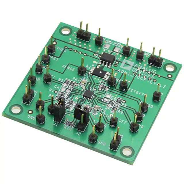
ADM1270CP-EVALZ/
ADM1270RQ-EVALZ User Guide
UG-760
One Technology Way • P.O. Box 9106 • Norwood, MA 02062-9106, U.S.A. • Tel: 781.329.4700 • Fax: 781.461.3113 • www.analog.com
Evaluating the ADM1270 High Voltage Input Protection Device
FEATURES
ADDITIONAL EQUIPMENT NEEDED
Controls supply voltages from 4 V to 60 V
Gate drive for low voltage drop reverse supply protection
Gate drive for P-channel field effect transistors (FETs)
Inrush current limiting control
Adjustable current limit
Foldback current limiting
Automatic retry or latch-off on current fault
Programmable current-limit timer for safe operating area (SOA)
Power-good and fault outputs
Analog undervoltage (UV) and overvoltage (OV) protection
16-lead, 3 mm × 3 mm LFCSP
16-lead QSOP
DC power supply
Multimeters for voltage and current measurements
Electronic or resistive loads
GENERAL DESCRIPTION
The ADM1270CP-EVALZ and ADM1270RQ-EVALZ evaluation
boards are used to demonstrate the functionality of the ADM1270
high voltage input protection device.
Full specifications on the ADM1270 are available in the product
data sheet, which should be consulted in conjunction with this
user guide when using these evaluation boards.
EVALUATION KIT CONTENTS
ADM1270CP-EVALZ or ADM1270RQ-EVALZ evaluation board
PLEASE SEE THE LAST PAGE FOR AN IMPORTANT
WARNING AND LEGAL TERMS AND CONDITIONS.
Rev. A | Page 1 of 12
�UG-760
ADM1270CP-EVALZ/ADM1270RQ-EVALZ User Guide
TABLE OF CONTENTS
Features .............................................................................................. 1
TIMER ............................................................................................5
Evaluation Kit Contents ................................................................... 1
TIMER_OFF ..................................................................................6
Additional Equipment Needed ....................................................... 1
Hot Swap Retry Duty Cycle .........................................................7
General Description ......................................................................... 1
Gate and RPFG Clamps ................................................................7
Revision History ............................................................................... 2
Fast Response to Severe Overcurrent .........................................7
Evaluation Board Hardware ............................................................ 3
Undervoltage and Overvoltage ....................................................7
Evaluation Board Configurations .............................................. 3
Enable Input ...................................................................................7
Configuring the ADM1270 ............................................................. 4
Power Good ...................................................................................8
Powering the ADM1270 .............................................................. 4
Evaluation Board Schematics and Artwork ...................................9
Current Sense Inputs.................................................................... 4
Ordering Information .................................................................... 12
Current-Limit Reference ............................................................. 4
Bill of Materials ........................................................................... 12
Setting the Current Limit (ISET) ............................................... 4
Foldback......................................................................................... 5
REVISION HISTORY
4/16—Rev. 0 to Rev. A
Change to Setting the Current Limit (ISET) Section................... 5
12/14—Revision 0: Initial Version
Rev. A | Page 2 of 12
�ADM1270CP-EVALZ/ADM1270RQ-EVALZ User Guide
UG-760
EVALUATION BOARD HARDWARE
EVALUATION BOARD CONFIGURATIONS
The ADM1270CP-EVALZ and ADM1270RQ-EVALZ evaluation boards arrive supplied with different components depending on which
version is ordered.
Table 1. Evaluation Board Hardware Components
Component
U11
C1
C2
C3
R1
R2
R3
R4
R5
R6
R7
R8
R9
R10
R11
R12
Q1A, Q1B
Function
High voltage protection device
VCAP bypass capacitor
TIMER capacitor
TIMER_OFF capacitor
OVLO/UVLO resistor divider
OVLO/UVLO resistor divider
OVLO/UVLO resistor divider
OC current-limit threshold
OC current-limit threshold
Current sense resistor
OC foldback divider
OC foldback divider
Power-good (PG) threshold
FAULT pull up
PWRGD pull up
ENABLE pull down
Protection FET
Q2, Q4
Q3, Q5
J1
J2
Protection FET
Protection FET
Jumper
Jumper
1
Description
ADM1270CP or ADM1270RQ high voltage protection device
1 μF, VCAP bypass capacitor
100 nF, CTIMER, sets an SOA overcurrent (OC) fault delay, nominally 100 ms
100 nF, CTIMER_OFF, sets an initial timing cycle delay and the SOA off time delay, nominally 200 ms
332 kΩ, sets UV threshold, nominally 8.7 V
33.2 kΩ, sets OV/UV thresholds with R1 and R3
10 kΩ, sets OV threshold, nominally 37.5 V
100 kΩ, sets OC threshold with R5, nominally 450 mA when R6 = 100 mΩ
100 kΩ, sets OC threshold with R4, nominally 450 mA when R6 = 100 mΩ
100 mΩ, current sense resistor for OC protection
4.75 kΩ, sets foldback threshold with R8, nominally 13.2 V
332 kΩ, sets foldback threshold with R7, nominally 13.2 V
20 kΩ, sets power-good threshold, nominally 18 V
332 kΩ, FAULT pin pull up
332 kΩ, PWRGD pin pull up
332 kΩ, ENABLE pin pull down
FDS9958 dual P-channel metal-oxide semiconductor field effect transistor (MOSFET),
−60 V/−2.9 A, 105 mΩ
DPAK FET (optional)
D2PAK FET (optional)
Connects ENABLE to VIN for automatic startup
Connect this pin directly to the ENABLE pin for automatic retry after shutdown
Component varies depending on the evaluation board ordered.
Rev. A | Page 3 of 12
�ADM1270CP-EVALZ/ADM1270RQ-EVALZ User Guide
CONFIGURING THE ADM1270
POWERING THE ADM1270
A supply voltage from 4 V to 60 V is required to power the
ADM1270 via the VCC/SENSE+ pin. The VCC/SENSE+ pin
provides the majority of the bias current for the device; the
remainder of the current needed to control the gate drive and to
best regulate the gate to source voltage (VGS) is supplied by the
SENSE− pin.
CURRENT SENSE INPUTS
RSENSE
VCC/SENSE+
VCAP
LDO
SENSE–
–
VCAP
LDO
Q1
+
GATE
–
–
2V
GATE
REF
SELECT
+
CURRENTLIMIT
CONTROL
FLB
CURRENT
LIMIT
–
GND
Figure 2. Current-Limit Reference Selection
VISET
FLB
CURRENT
LIMIT
GND
+
Q1
40×
2V
12660-001
+
SENSE–
The FLB voltage varies during different modes of operation
and, therefore, is clamped to a minimum level of 200 mV. This
behavior prevents zero current flow due to the current limit
being set too low. Figure 3 provides an example of how the FLB
and ISET voltages interact during startup as the ADM1270
turns on the FET and charges the load capacitance. Depending
on how the foldback feature is configured, the transition point
varies to ensure that the FET operates within the correct limits.
40×
REFERENCE
VCC/SENSE+
ISET
The load current is monitored by measuring the voltage drop
across an external current sense resistor, RSENSE (see Figure 1).
An internal current sense amplifier provides a gain of 40 to the
voltage drop detected across RSENSE. The result is compared to an
internal reference and is used by the hot swap control logic to
detect an overcurrent condition.
4V TO 60V
RSENSE
4V TO 60V
12660-002
UG-760
ISET
CURRENT-LIMIT
REFERENCE
Figure 1. Hot Swap Current Sense Amplifier
CURRENT-LIMIT REFERENCE
The current-limit reference voltage determines the load current
at which the ADM1270 limits the current during an overcurrent
event. This reference voltage is compared to the amplified current
sense voltage to determine when the current-limit threshold is
reached.
An internal current-limit reference selector block continuously
compares the current-limit (ISET) and foldback (FLB) voltages
to determine which voltage is the lowest at any given time; the
lowest voltage is used as the current-limit reference. This behavior
ensures that the programmed current limit, ISET, is used in normal
operation, and that the foldback feature reduces the current
limit when required during startup and/or fault conditions.
TIME
12660-003
0.2V
Figure 3. Interaction of Foldback (FLB) and ISET Current Limits
SETTING THE CURRENT LIMIT (ISET)
The maximum current limit is partially determined by selecting
a sense resistor to match the current sense voltage limit on the
controller for the desired load current. However, as currents
become larger, the sense resistor value decreases for a given
current sense voltage. Choosing an appropriate current sense
resistor can be difficult due to the limited selection of low value
resistors. The ADM1270 provides an adjustable current sense
voltage limit to handle this issue. The device allows the user to
program the required current sense voltage limit from 12.5 mV
to 62.5 mV.
Rev. A | Page 4 of 12
�ADM1270CP-EVALZ/ADM1270RQ-EVALZ User Guide
FOLDBACK
The default value is 50 mV and is achieved by connecting the
ISET pin directly to the VCAP pin. This circuit configuration
configures the device to use an internal 2 V reference, which
results in 50 mV at the sense inputs (see Figure 4).
VCC/SENSE+
VCAP
Foldback is a method to actively reduce the current limit as the
voltage drop across the FET increases. This technique keeps the
power dissipation in the FET at a minimum during power-up,
overcurrent, or short-circuit events. It also reduces the need to
oversize the FET to accommodate worst-case conditions,
resulting in board size and cost savings.
RSENSE
4V TO 60V
LDO
SENSE–
+
Q1
Assuming that the supply voltage remains constant and within
tolerance, the ADM1270 detects the voltage drop across the FET
by sensing output voltage through a resistor divider. The device,
therefore, relies on the principle that the drain of the FET is at
the maximum expected supply voltage, and that the magnitude
of the output voltage is relative to that of the VDS of the FET.
Using a resistor divider from the output voltage to the FLB pin,
the relationship from VOUT, and thus VDS, to VFLB can be derived.
–
40×
2V
ISET
GATE
REF
SELECT
+
CURRENTLIMIT
CONTROL
12660-004
FLB
CURRENT
LIMIT
–
GND
Figure 4. Fixed 50 mV Current Sense Limit
To program the sense voltage from 12.5 mV to 62.5 mV, an
external resistor divider sets the reference voltage on the
ISET pin (see Figure 5).
RSENSE
4V TO 60V
VCC/SENSE+
VCAP
LDO
SENSE–
+
Q1
–
GATE
REF
SELECT
+
FLB
CURRENTLIMIT
CONTROL
–
CURRENT
LIMIT
GND
12660-005
ISET
Design the resistor divider to result in a voltage equal to VISET/2
when VOUT falls below the desired level. This voltage must be
well below the working tolerance of the supply rail. As VOUT
continues to drop, the current-limit reference follows VFLB
because it is now the lowest voltage input to the current-limit
reference selector block, resulting in a reduction of the current
limit and, therefore, the regulated load current. To prevent the
current from decreasing to zero, a clamp activates when VFLB
reaches 200 mV. The current limit cannot drop below this level.
To ensure that the SOA characteristics of a particular FET are
not violated, the minimum current for this clamp varies from
design to design. However, the current-limit reference fixes this
clamp at 200 mV, which equals 10 mV across the sense resistor.
Therefore, the main ISET voltage can be adjusted to adjust the
clamp to the required percentage current reduction. For example,
if VISET equals 1.6 V, set the clamp at 25% of the maximum current.
40×
2V
UG-760
Figure 5. Adjustable 12.5 mV to 62.5 mV Current Sense Limit
The VCAP pin has a 3.6 V internally generated voltage that can
set a voltage at the ISET pin. Assuming that VISET equals the
voltage on the ISET pin, select the resistor divider values to set
the ISET voltage as follows:
TIMER
An essential block of the ADM1270 is the TIMER function,
which limits the time the current is in regulation during an
overcurrent event. MOSFETs are designed to withstand a given
amount of power for a prescribed maximum time. The MOSFET
manufacturers outline this range, or SOA, using a graph such as
that shown in Figure 6.
20
VISET = VSENSE × 40
0.1ms
10
–ID, DRAIN CURRENT (A)
where VSENSE is the current sense voltage limit.
The VCAP rail also can be used as the pull-up supply for setting
other pins. To guarantee that VCAP meets its accuracy
specifications, do not apply a load to the VCAP pin greater
than 100 µA.
1ms
1
10ms
THIS AREA IS
LIMITED BY rDS(on)
0.1
100ms
SINGLE PULSE
TJ = MAX RATED
RθJA = 135°C/W
TA = 25°C
1s
10s
1
10
–VDS, DRAIN TO SOURCE VOLTAGE (V)
Figure 6. MOSFET SOA Graph
Rev. A | Page 5 of 12
100 200
12660-006
DC
0.01
0.1
�UG-760
ADM1270CP-EVALZ/ADM1270RQ-EVALZ User Guide
The SOA graph shows a relationship between the combined
drain to source voltage, the drain current, and the time duration
that the MOSFET can withstand this dissipation. For example,
the MOSFET in Figure 6 can withstand 60 V and 2 A (120 W)
for 1 ms. If this condition persists for a greater duration, the
MOSFET may be damaged. The TIMER circuit can ensure that
the length of time the MOSFET is subject to these worst-case
conditions is limited by the external TIMER capacitor. For
example, if the TIMER is set to 1 ms, and the current exceeds
the limit for more than 1 ms, the circuit times out and shuts
down the MOSFET.
The TIMER pin handles the timing function with an external
capacitor, CTIMER. The two TIMER pin comparator thresholds
are VTIMERL (0.1 V) and VTIMERH (2.0 V). There are two timing
current sources as well: a 20 µA pull-up current and a 1 µA
pull-down current.
These current and voltage levels, in combination with the user
chosen value of CTIMER, determine the fault current-limit time
and the on-time of the hot swap retry duty cycle. The TIMER
pin capacitor value is determined using the following equation:
CTIMER = (tON × 20 µA)/VTIMERH
where:
tON is the time that the FET is allowed to spend in regulation at
the current limit.
VTIMERH is the TIMER high threshold.
The choice of FET is based on matching this time with the SOA
characteristics of the FET. Foldback can also be used to simplify
the selection.
When the voltage across the sense resistor reaches the circuit
breaker trip voltage, VCB, the 20 µA TIMER pull-up current is
activated. The ADM1270 begins to regulate the load current at
the current limit, initiating a rising voltage ramp on the TIMER
pin. If the sense voltage falls below this circuit breaker trip voltage
before the TIMER pin reaches VTIMERH, the 20 µA pull-up current is
disabled, and the 1 µA pull-down current is enabled. If the voltage
on the TIMER pin falls below VTIMERL, the TIMER pin is
discharged to GND using a strong pull-down current on the
TIMER pin.
The circuit breaker trip voltage is not the same as the hot swap
sense voltage current limit. There is a small circuit breaker
offset, VCBOS, which causes the timer to start a short time before
the current reaches the defined current limit.
However, if the overcurrent condition is continuous and the sense
voltage remains above the circuit breaker trip voltage, the 20 µA
pull-up current remains active, and the FET remains in regulation.
This condition allows the TIMER pin to reach VTIMERH and to
initiate the GATE shutdown, and the FAULT pin is pulled low
immediately.
The circuit breaker trip voltage is not the same as the hot swap
sense voltage current limit. There is a small circuit breaker offset,
VCBOS, which causes the timer to start shortly before the current
reaches the defined current limit.
In latch-off mode, the TIMER pin is discharged to GND when
it reaches the VTIMERH threshold. The TIMER_OFF pin begins to
charge up. While the TIMER_OFF pin is ramping up, the hot swap
controller remains off and cannot be turned back on, and the
FAULT pin remains low. When the voltage on the TIMER_OFF
pin rises above the VTMROFFH threshold, the hot swap controller
can be reenabled by toggling the ENABLE pin from high to low
and then high again.
TIMER_OFF
The TIMER_OFF pin handles two timing functions with an
external capacitor, CTIMER_OFF. There is one TIMER_OFF pin
comparator threshold at VTMROFFH (2.0 V). There are two timing
current sources, a 20 µA pull-up current and a 1 µA pull-up
current.
These current and voltage levels, in combination with the user
chosen value of CTIMER_OFF, determine the initial power-on reset
time and also set the fault current-limit off time.
When VCC is connected to the input supply, the internal supply
(VCAP) of the ADM1270 must charge up. VCAP starts up and
settles in a very short time. When the UVLO threshold voltage is
exceeded at VCAP, the device emerges from reset. During this first
brief reset period, the GATE and TIMER pins are both held low.
The ADM1270 then proceeds through an initial timing cycle.
The TIMER_OFF pin is pulled high with 20 µA. When the
TIMER_OFF pin reaches the VTMROFFH threshold (2.0 V), the
initial timing cycle is complete. This initial power-on reset
duration is determined by the following equation:
tINITIAL = VTMROFFH × (CTIMER_OFF/20 µA)
For example, a 100 nF capacitor results in a delay of approximately
10 ms. If the UV and OV inputs indicate that VCC is within the
defined window of operation when the initial timing cycle
terminates, the device is ready to start a hot swap operation.
At the completion of this initial power-on reset cycle, the
TIMER_OFF pin is ready to perform a second function. When
the voltage at the TIMER pin exceeds the fault current-limit
time threshold voltage of VTIMERH (2.0 V), the 1 µA pull-up
current is activated on TIMER_OFF, and CTIMER_OFF begins to
charge initiating a voltage ramp on the TIMER_OFF pin. When
the TIMER_OFF pin reaches VTMROFFH, the TIMER_OFF fault
current-limit off time is complete.
This fault current-limit off time is determined by the following
equation:
tTIMER_OFF = VTMROFFH × (CTIMER_OFF/1 µA)
For example, a 100 nF capacitor results in an off time of
approximately 200 ms from the time that TIMER exceeds
VTIMERH to the time that TIMER_OFF reaches VTMROFFH.
Rev. A | Page 6 of 12
�ADM1270CP-EVALZ/ADM1270RQ-EVALZ User Guide
The ADM1270 turns off the FET after an overcurrent fault and
then uses the capacitor on the TIMER_OFF pin to generate a
delay before automatically retrying the hot swap operation. To
configure the ADM1270 for automatic retry mode, tie the FAULT
pin to the ENABLE pin. Note that a pull-up resistor to VCAP is
required on the FAULT pin.
When an overcurrent fault occurs, the capacitor on the TIMER
pin charges with a 20 µA pull-up current. When the TIMER pin
reaches VTIMERH (2.0 V), the GATE pin is pulled high, turning
off the FET. When the FAULT pin is tied to the ENABLE pin
for automatic retry mode, the TIMER_OFF pin begins to
charge with a 1 µA current source. When the TIMER_OFF pin
reaches VTMROFFH (2.0 V), the ADM1270 automatically restarts
the hot swap operation.
The automatic retry duty cycle is set by the ratio of 1 µA/20 µA
and the ratio of CTIMER/CTIMER_OFF. The retry duty cycle is set by
the following equation:
Duty_Cycle = (CTIMER × 1 µA)/( CTIMER_OFF × 20 µA)
The value of the CTIMER and CTIMER_OFF capacitors
determine the on and off time of this cycle, which are calculated
as follows:
tON = VTIMERH × (CTIMER/20 µA)
tOFF = VTMROFFH × (CTIMER_OFF/1 µA)
efficiency and more headroom for operation. Refer to the
ADM1270 data sheet for the connection of Q2 and RPFG for
proper operation.
FAST RESPONSE TO SEVERE OVERCURRENT
The ADM1270 includes a separate, high bandwidth, current
sense amplifier to detect a severe overcurrent that is indicative of
a short circuit. The fast response time allows the ADM1270 to
handle events of this type that could otherwise cause catastrophic
damage if not detected and dealt with very quickly. The fast
response circuit ensures that the ADM1270 can detect an
overcurrent event of approximately 200% of the normal current
limit and control the current within approximately 2 µs.
UNDERVOLTAGE AND OVERVOLTAGE
The ADM1270 monitors the supply voltage for UV and OV
conditions. The UV and OV pins are connected to the inputs
of the voltage comparators and compared to an internal 1 V
voltage reference.
Figure 7 illustrates the voltage monitoring input connections.
An external resistor network divides the supply voltage for
monitoring. An undervoltage event is detected when the voltage
connected to the UV pin falls below 1 V, and the FET is turned
off using the 10 mA pull-up current. Similarly, when an overvoltage
event occurs and the voltage on the OV pin exceeds 1 V, the
FET is turned off using the 10 mA pull-up current.
4V TO 60V
A 100 nF capacitor on the TIMER pin gives an on time of
10 ms. A 100 nF capacitor on the TIMER_OFF pin gives an off
time of 200 ms. The device retries continuously in this manner
and can be disabled manually by holding the ENABLE pin low,
or by disconnecting the FAULT pin. To prevent thermal stress
in the FET, a capacitor on the TIMER_OFF pin can be used to
extend the retry time to any desired level.
VCC/SENSE+
LDO
UV
–
40×
–
GATE DRIVE/
LOGIC
OV
The circuits driving the GATE and RPFG pins are clamped to less
than 14 V below the VCC/SENSE+ pin. These clamps ensure that
the maximum VGS rating of the external FETs is not exceeded.
Q1
+
1V
In the typical case where power is applied to VCC, the gate is
still pulled down and allows the FET Q2 to turn on and conduct
current in the forward direction. Operating Q2 in this way
provides a low on-resistance, low voltage drop compared to a
diode for reverse polarity protection, giving the system higher
SENSE–
+
VCAP
GATE AND RPFG CLAMPS
The reverse protection FET gate pin (RPFG) drives the gate of
an external PMOSFET. This PMOSFET, Q2, provides reverse
polarity protection to the ADM1270 and the system being
powered. If the VCC and GND pins have been reverse
connected (that is, where power is actually applied to GND),
VCC is negative with respect to the system ground. In this
condition, Q2 prevents current from flowing in the reverse
direction because the gate of Q2 is held at GND, and Q2 is off.
VOUT is not pulled below GND, and the system is protected
against a reverse polarity connection.
RSENSE
–
1V
GATE
+
GND
12660-007
HOT SWAP RETRY DUTY CYCLE
UG-760
Figure 7. Undervoltage and Overvoltage Supply Monitoring
ENABLE INPUT
The ADM1270 provides a dedicated ENABLE digital input pin.
The ENABLE pin allows the ADM1270 to remain off by using a
hardware signal, even when the voltage on the UV pin is greater
than 1.0 V, and the voltage on the OV pin is less than 1.0 V.
Although the UV pin can be used to provide a digital enable
signal, using the ENABLE pin for this purpose keeps the ability
of the UV pin free to monitor undervoltage conditions.
In addition to the conditions for the UV and OV pins, the
ADM1270 ENABLE input pin must be high for the device to
begin a power-up sequence.
Rev. A | Page 7 of 12
�UG-760
ADM1270CP-EVALZ/ADM1270RQ-EVALZ User Guide
A similar function can be achieved using the UV pin directly.
Alternatively, if the UV divider function is still required, the
configuration shown in Figure 8 can be used.
RSENSE
4V TO 60V
VCC/SENSE+
SENSE–
Q1
VIN
+
ADM1270
VCAP
UV
R1
EN
D1
LDO
+
1V
UV
OV
R2
–
40×
–
GATE DRIVE/
LOGIC
–
1V
+
GATE
FB_PG
12660-008
GND
Figure 9. Generation of PWRGD Signal
Figure 8. Using the UV Pin as an Enable
Diode D1 prevents the external driver pull-up resistor from
affecting the UV threshold. Select Diode D1 using the following
criteria:
(VF × D1) + (VOL × EN)