5.7 kV rms, Signal Isolated,
Basic CAN FD Transceiver
ADM3050E-EP
FEATURES
FUNCTIONAL BLOCK DIAGRAM
5.7 kV rms signal isolated CAN FD transceiver
1.7 V to 5.5 V supply and logic side levels
4.5 V to 5.5 V supply on bus side
ISO 11898-2:2016-compliant CAN FD
Data rates up to 12 Mbps for CAN FD
Low maximum loop propagation delay: 145 ns
Extended common-mode range (VCANx): ±25 V
Bus fault protection (CANH, CANL): ±40 V
Passes EN 55022, Class B by 6 dB
Safety and regulatory approvals
VDE certificate of conformity, VDE V 0884-10 (pending)
UL: 5700 V rms for 1-minute duration per UL 1577 (pending)
CSA component acceptance 5A at 5.7 kV rms
IEC 60950, IEC 61010 (pending)
High CMTI: >75 kV/µs
VDD1
VDD2
ADM3050E-EP
CAN
TRANSCEIVER
DIGITAL ISOLATOR
DOMINANT
TIMEOUT
TXD
CANH
RXD
CANL
THERMAL
SHUTDOWN
GND2
GND1
17317-001
Enhanced Product
Figure 1.
ENHANCED PRODUCT FEATURES
Supports defense and aerospace applications (AQEC standard)
Military temperature range (−55°C to +125°C)
Controlled manufacturing baseline
1 assembly/test site
1 fabrication site
Product change notification
Qualification data available on request
APPLICATIONS
CANOpen, DeviceNet, and other CAN bus implementations
Industrial automation
Military and aerospace (MILA) avionics for sensors,
actuators, and engine control
GENERAL DESCRIPTION
The ADM3050E-EP is a 5.7 kV rms isolated controller area
network (CAN) physical layer transceiver with a high
performance, basic feature set. The ADM3050E-EP fully meets
the CAN flexible data rate (CAN FD) ISO 11898-2:2016
requirements and is further capable of supporting data rates as
high as 12 Mbps.
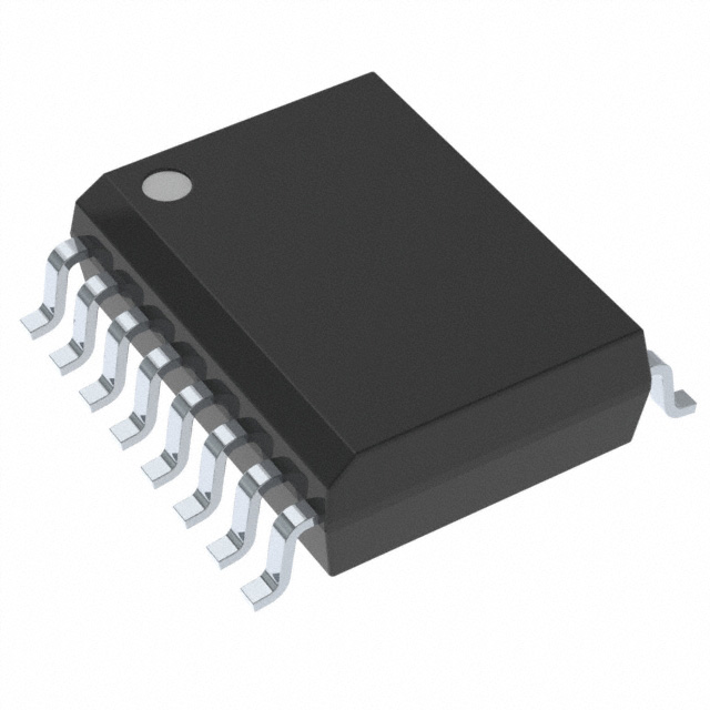
The device employs Analog Devices, Inc., iCoupler® technology
to combine a 2-channel isolator and a CAN transceiver into a
single small outline integrated circuit (SOIC) surface-mount
package. The ADM3050E-EP is a fully isolated solution for CAN
and CAN FD applications. The ADM3050E-EP provides
isolation between the CAN controller and physical layer bus.
Safety and regulatory approvals (pending) for a 5.7 kV rms
Rev. 0
withstand voltage, an 849 VPEAK working voltage, and a 12.8 kV
surge test, ensure that the ADM3050E-EP meets application
isolation requirements.
Low loop propagation delays and the extended common-mode
range of ±25 V support robust communication on longer bus
cables. Dominant timeout functionality protects against bus
lock up in a fault condition, and current limiting and thermal
shutdown features protect against output short circuits. The
CAN bus input and output pins are protected to ±40 V against
accidental connection to a +24 V bus supply. The device is fully
specified over the −55°C to +125°C industrial temperature range.
Additional application and technical information can be found
in the ADM3050E data sheet.
Document Feedback
Information furnished by Analog Devices is believed to be accurate and reliable. However, no
responsibility is assumed by Analog Devices for its use, nor for any infringements of patents or other
rights of third parties that may result from its use. Specifications subject to change without notice. No
license is granted by implication or otherwise under any patent or patent rights of Analog Devices.
Trademarks and registered trademarks are the property of their respective owners.
One Technology Way, P.O. Box 9106, Norwood, MA 02062-9106, U.S.A.
Tel: 781.329.4700
©2019 Analog Devices, Inc. All rights reserved.
Technical Support
www.analog.com
�ADM3050E-EP
Enhanced Product
TABLE OF CONTENTS
Features .............................................................................................. 1
Enhanced Product Features ............................................................ 1
DIN V VDE V 0884-10 (VDE V 0884-10) Insulation
Characteristics (Pending) .............................................................7
Applications ....................................................................................... 1
Absolute Maximum Ratings ............................................................8
Functional Block Diagram .............................................................. 1
Thermal Resistance .......................................................................8
General Description ......................................................................... 1
ESD Caution...................................................................................8
Revision History ............................................................................... 2
Pin Configuration and Function Descriptions..............................9
Specifications..................................................................................... 3
Operational Truth Table ...............................................................9
Timing Specifications .................................................................. 5
Typical Performance Characteristics ........................................... 10
Insulation and Safety Related Specifications ............................ 6
Test Circuits ..................................................................................... 12
Package Characteristics ............................................................... 6
Outline Dimensions ....................................................................... 13
Regulatory Information ............................................................... 6
Ordering Guide .......................................................................... 13
REVISION HISTORY
2/2019—Revision 0: Initial Version
Rev. 0 | Page 2 of 13
�Enhanced Product
ADM3050E-EP
SPECIFICATIONS
All voltages are relative to their respective ground, 1.7 V ≤ VDD1 ≤ 5.5 V, 4.5 V ≤ VDD2 ≤ 5.5 V, and −55°C ≤ TA ≤ +125°C, unless otherwise
noted. Typical specifications are at VDD1 = VDD2 = 5 V and TA = 25°C, unless otherwise noted.
Table 1.
Parameter
SUPPLY CURRENT
Bus Side
Recessive State
Dominant State
70% Dominant/30% Recessive
1 Mbps
5 Mbps
12 Mbps
Logic Side iCoupler Current
DRIVER
Differential Outputs
Recessive State Voltage
CANH, CANL
Differential Output
Dominant State Voltage
CANH
CANL
Differential Output
Output Symmetry (VDD2 − VCANH to VCANL)
Short-Circuit Current
Absolute
CANH
CANL
Steady State
CANH
CANL
Logic Input TXD
Input Voltage
High
Low
Complementary Metal-Oxide
Semiconductor (CMOS) Logic Input
Currents
RECEIVER
Differential Inputs
Differential Input Voltage Range
Recessive
Dominant
Input Voltage Hysteresis
Unpowered Input Leakage Current
Symbol
Min
Typ
Max
Unit
Test Conditions/Comments
5.3
63
7
75
mA
mA
73
mA
TXD high, load resistance (RL) = 60 Ω
Limited by transmit dominant timeout
(tDT), RL = 60 Ω
Limited by tDT, RL = 60 Ω, 4.75 V ≤ VDD2 ≤
5.25 V
Worst case, RL = 60 Ω
58
60
65
5.5
mA
mA
mA
mA
IDD2
45
49
58
IDD1
TXD high, low, or switching
See Figure 18
TXD high, RL, and common-mode filter
capacitor (CF) open
VCANL, VCANH
VOD
2.0
−500
3.0
+50
V
mV
VCANH
VCANL
VOD
2.75
0.5
1.5
1.4
1.5
−0.55
4.5
2.0
3.0
3.3
5.0
+0.55
V
V
V
V
V
V
TXD low, CF open
50 Ω ≤ RL ≤ 65 Ω
50 Ω ≤ RL ≤ 65 Ω
50 Ω ≤ RL ≤ 65 Ω
45 Ω ≤ RL ≤ 70
RL = 2240 Ω
RL = 60 Ω, CF = 4.7 nF
RL open
115
115
mA
mA
VCANH = −3 V
VCANL = 18 V
115
115
mA
mA
VCANH = −24 V
VCANL = 24 V
0.35 × VDD1
10
V
V
µA
Input high or low
VSYM
|ISC|
VIH
VIL
|IIH|, |IIL|
0.65 × VDD1
VID
See Figure 19, RXD capacitance (CRXD)
open, −25 V < VCANL, VCANH < +25 V
−1.0
0.9
VHYS
|IIN (OFF)|
+0.5
5.0
150
10
Rev. 0 | Page 3 of 13
V
V
mV
µA
VCANH, VCANL = 5 V, VDD2 = 0 V
�ADM3050E-EP
Parameter
Input Resistance
CANH, CANL
Differential
Input Resistance Matching
CANH, CANL Input Capacitance
Differential Input Capacitance
Logic Output (RXD)
Output Voltage
Low
High
Short-Circuit Current
COMMON-MODE TRANSIENT IMMUNITY
(CMTI)1
Input High, Recessive
Input Low, Dominant
1
Enhanced Product
Symbol
Min
RINH, RINL
RDIFF
mR
CINH, CINL
CDIFF
6
20
−0.03
Typ
Max
Unit
25
100
+0.03
kΩ
kΩ
35
12
0.2
Test Conditions/Comments
mR = 2 × (RINH − RINL)/(RINH + RINL)
pF
pF
VOL
VOH
IOS
VDD1 − 0.2
7
0.4
|CMH|
75
100
kV/µs
|CML|
75
100
kV/µs
85
V
V
mA
Output impedance (IOUT) = 2 mA
IOUT = −2 mA
Output voltage (VOUT) = GND1 or VDD1
Common-mode voltage (VCM) ≥ 1 kV,
transient magnitude ≥ 800 V
Input voltage (VIN) = VDD1 (TXD) or
CANH/CANL recessive
VIN = 0 V (TXD) or CANH/CANL dominant
|CMH| is the maximum common-mode voltage slew rate that can be sustained while maintaining CANH/CANL recessive or RXD ≥ VDD1 − 0.2 V. |CML| is the maximum
common-mode voltage slew rate that can be sustained while maintaining CANH/CANL dominant or RXD ≤ 0.4 V. The common-mode voltage slew rates apply to both
rising and falling common-mode voltage edges.
Rev. 0 | Page 4 of 13
�Enhanced Product
ADM3050E-EP
TIMING SPECIFICATIONS
All voltages are relative to their respective ground, 1.7 V ≤ VDD1 ≤ 5.5 V, 4.5 V ≤ VDD2 ≤ 5.5 V, and −55°C ≤ TA ≤ +125°C, unless otherwise
noted. Typical specifications are at VDD1 = VDD2 = 5 V and TA = 25°C, unless otherwise noted. See the ADM3050E data sheet for
information about tBIT_BUS.
Table 2.
Parameter
DRIVER
Symbol
Min
Maximum Data Rate
Typ
Max
Unit
12
Propagation Delay from TXD to Bus (Recessive to Dominant)
Propagation Delay from TXD to Bus (Dominant to Recessive)
Transmit Dominant Timeout
RECEIVER
tTXD_DOM
tTXD_REC
tDT
Falling Edge Loop Propagation Delay (TXD to RXD)
Rising Edge Loop Propagation Delay (TXD to RXD)
Loop Delay Symmetry (Minimum Recessive Bit Width)
2 Mbps
5 Mbps
8 Mbps
12 Mbps
tLOOP_FALL
tLOOP_RISE
tBIT_RXD
Mbps
35
45
1175
450
160
85
50
60
70
4000
ns
ns
µs
145
145
ns
ns
550
220
140
91.6
ns
ns
ns
ns
Timing Diagrams
TXD
0.7VDD1
0.3VDD1
VDD1
0.3VDD1
0V
5 × tBIT_TXD
tBIT_TXD
tLOOP_FALL
0.9V
0.5V
tTXD_REC
tBIT_BUS
tTXD_DOM
0.7VDD1
RXD
0.3VDD1
tBIT_RXD
VDD1
0V
tLOOP_RISE
Figure 2. Transceiver Timing Diagram
tDT
17317-103
TXD
VOD
Figure 3. Dominant Timeout, tDT
Rev. 0 | Page 5 of 13
17317-002
VOD/VID
Test Conditions/Comments
See Figure 2 and Figure 18,
tBIT_TXD = 200 ns, RL = 60 Ω,
CL = 100 pF
TXD low, see Figure 3
See Figure 2 and Figure 20,
tBIT_TXD = 200 ns, RL = 60 Ω,
CL = 100 pF, CRXD = 15 pF
tBIT_TXD = 500 ns
tBIT_TXD = 200 ns
tBIT_TXD = 125 ns
tBIT_TXD = 83.3 ns
�ADM3050E-EP
Enhanced Product
INSULATION AND SAFETY RELATED SPECIFICATIONS
For additional information, see www.analog.com/icouplersafety.
Table 3.
Parameter
Rated Dielectric Insulation Voltage
Minimum External Air Gap (Clearance)
Symbol
L (I01)
Value
5700
7.8
Unit
V rms
mm min
Minimum External Tracking (Creepage)
L (I02)
7.8
mm min
Minimum Clearance in the Plane of the Printed
Circuit Board (PCB) Clearance
L (PCB)
8.3
mm min
CTI
25.5
>600
I
µm min
V
Minimum Internal Gap (Internal Clearance)
Tracking Resistance (Comparative Tracking Index)
Material Group
Test Conditions/Comments
1-minute duration
Measured from input terminals to output terminals,
shortest distance through air
Measured from input terminals to output terminals,
shortest distance path along body
Measured from input terminals to output terminals,
shortest distance through air, line of sight, in the PCB
mounting plane
Insulation distance through insulation
DIN IEC 112/VDE 0303 Part 1
Material group (DIN VDE 0110, 1/89, Table 1)
PACKAGE CHARACTERISTICS
Table 4.
Parameter
Resistance (Input to Output)1
Capacitance (Input to Output)1
Input Capacitance2
1
2
Symbol
RI-O
CI-O
CI
Min
Typ
1013
1.1
4.0
Max
Unit
Ω
pF
pF
Test Conditions/Comments
f = 1 MHz
The device is considered a two-terminal device: Pin 1 through Pin 8 are shorted together, and Pin 9 through Pin 16 are shorted together.
Input capacitance is from any input data pin to ground.
REGULATORY INFORMATION
See Table 9 and the ADM3050E data sheet for the recommended maximum working voltages for specific cross isolation waveforms and
insulation levels. The ADM3050E-EP is pending approval or approved by the organizations listed in Table 5.
Table 5.
UL (Pending)
CSA (Pending)
VDE (Pending)
CQC (Pending)
UL1577 Component
Recognition Program1
Approved under CSA Component
Acceptance Notice 5A
DIN V VDE V 0884-10
(VDE V 0884-10):2006-122
Certified under CQC11471543-2012
Single Protection, 5700 V rms
Isolation Voltage
CSA 60950-1-07+A1+A2 and
IEC 60950-1, second edition, +A1+A2:
Reinforced insulation,
849 VPEAK, VIOTM = 8 kVPEAK
GB4943.1-2011
Basic insulation at 780 V rms (1103 VPEAK)
Basic insulation at 780 V rms
(1103 VPEAK)
Reinforced insulation at
390 V rms (552 VPEAK)
Reinforced insulation at 390 V rms (552 VPEAK)
IEC 60601-1 Edition 3.1:
Basic insulation (1 MOPP), 490 V rms
(686 VPEAK)
Reinforced insulation (2 MOPP), 238 V rms
(325 VPEAK)
CSA 61010-1-12 and IEC 61010-1 third edition:
Basic insulation at: 300 V rms mains, 780 V
secondary (1103 VPEAK)
Reinforced insulation at: 300 V rms mains,
390 V secondary (552 VPEAK)
File E214100
1
2
File 205078
File 2471900-4880-0001
File (pending)
In accordance with UL 1577, each ADM3050E-EP is proof tested by applying an insulation test voltage ≥ 6840 V rms for 1 sec.
In accordance with DIN V VDE V 0884-10, each ADM3050E-EP is proof tested by applying an insulation test voltage ≥ 1592 V peak for 1 sec (partial discharge detection limit =
5 pC). The * marking branded on the component designates DIN V VDE V 0884-10 approval.
Rev. 0 | Page 6 of 13
�Enhanced Product
ADM3050E-EP
DIN V VDE V 0884-10 (VDE V 0884-10) INSULATION CHARACTERISTICS (PENDING)
These isolators are suitable for reinforced electrical isolation only within the safety limit data. Protective circuits ensure the maintenance
of the safety data.
Table 6.
Description
Installation Classification per DIN VDE 0110
For Rated Mains Voltage ≤ 150 V rms
For Rated Mains Voltage ≤ 300 V rms
For Rated Mains Voltage ≤ 600 V rms
Climatic Classification
Pollution Degree per DIN VDE 0110, Table 1
Maximum Working Insulation Voltage
Reinforced
Basic, DC Working Voltage
Test Conditions/Comments
Symbol
Characteristic
Unit
I to IV
I to IV
I to IV
40/125/21
2
See the Absolute Maximum Ratings section and Table 9 for
the maximum continuous working voltage for ac bipolar,
ac unipolar, and dc voltages, basic and reinforced insulation,
and 50 year lifetime to 1% failure
VIORM × 1.875 = Vpd (m), 100% production test, tini = tm = 1 sec,
partial discharge < 5 pC
Input to Output Test Voltage, Method B1
Input to Output Test Voltage, Method A
After Environmental Tests Subgroup 1
VIORM
VIORM(DC)
849
1500
VPEAK
VDC
Vpd (m)
1592
VPEAK
1274
VPEAK
1019
VPEAK
VIOTM
VIMPULSE
8000
8000
VPEAK
VPEAK
VIOSM
VIOSM
12000
8000
VPEAK
VPEAK
VPEAK
TS
PS
RS
150
2.08
>109
°C
W
Ω
Vpd (m)
VIORM × 1.5 = Vpd (m), tini = 60 sec, tm = 10 sec,
partial discharge < 5 pC
VIORM × 1.2 = Vpd (m), tini = 60 sec, tm = 10 sec,
partial discharge < 5 pC
After Input and/or Safety Test
Subgroup 2 and Subgroup 3
Highest Allowable Overvoltage
Impulse
1.2 µs rise time, 50 µs, 50% fall time in air to the preferred
sequence
Surge Isolation Voltage
Basic
Reinforced
Safety Limiting Values
Maximum Junction Temperature
Total Power Dissipation at 25°C
Insulation Resistance at TS
VPEAK = 12.8 kV, 1.2 µs rise time, 50 µs, and 50% fall time
VPEAK = 12.8 kV, 1.2 µs rise time, 50 µs, and 50% fall time
Maximum value allowed in the event of a failure (see Figure 4)
Test voltage = 500 V
SAFE LIMITING POWER (W)
2.5
2.0
1.5
1.0
0
0
50
100
150
AMBIENT TEMPERATURE (°C)
200
14971-104
0.5
Figure 4. Thermal Derating Curve, Dependence of Safety Limiting Values with Ambient Temperature per DIN V VDE V 0884-10 (See the Thermal Resistance Section for
Additional Information)
Rev. 0 | Page 7 of 13
�ADM3050E-EP
Enhanced Product
ABSOLUTE MAXIMUM RATINGS
THERMAL RESISTANCE
Pin voltages with respect to GND1/GND2 are on same side,
unless otherwise noted.
Table 7.
Parameter
VDD1/VDD2
Logic Side Input and Output: TXD, RXD
CANH, CANL
Operating Temperature Range
Storage Temperature Range
Maximum Junction Temperature (TJ)
Electrostatic Discharge (ESD),
IEC 61000-4-2, CANH/CANL
Across Isolation Barrier with Respect
to GND1
Contact Discharge with Respect to
GND2
Air Discharge with Respect to GND2
Human Body Model (HBM), All Pins,
1.5 kΩ, 100 pF
Moisture Sensitivity Level (MSL)
Rating
−0.5 V to +6 V
−0.5 V to VDD1 + 0.5 V
−40 V to +40 V
−55°C to +125°C
−65°C to +150°C
150°C
Thermal performance is directly linked to PCB design and
operating environment. Careful attention to PCB thermal
design is required.
The thermal resistance value specified in Table 8 is simulated
based on JEDEC specifications (unless specified otherwise) and
must be used in compliance with JESD51-12.
Table 8. Thermal Resistance
Package Type
RW-161
1
±8 kV
θJA
60
Unit
°C/W
The θJA value is based on simulations of a devices mounted on a JEDEC
standard, 4-layer board with fine width traces and still air. See the
ADM3050E data sheet for the thermal model definitions.
±8 kV typical
ESD CAUTION
±15 kV
±4 kV
MSL3
Stresses at or above those listed under Absolute Maximum
Ratings may cause permanent damage to the product. This is a
stress rating only; functional operation of the product at these
or any other conditions above those indicated in the operational
section of this specification is not implied. Operation beyond
the maximum operating conditions for extended periods may
affect product reliability.
Table 9. Maximum Continuous Working Voltage1
Parameter
AC Voltage
Bipolar Waveform
Basic Insulation
Reinforced Insulation
Unipolar Waveform
Basic Insulation
Reinforced Insulation
DC Voltage
Basic Insulation
Reinforced Insulation
1
2
Insulation Rating (20-Year Lifetime)2
VDE 0884-11 Lifetime Conditions Fulfilled
849 VPEAK
707 VPEAK
Lifetime limited by insulation lifetime per VDE-0884-11
Lifetime limited by insulation lifetime per VDE-0884-11
1697 VPEAK
1275 VPEAK
Lifetime limited by insulation lifetime per VDE-0884-11
Lifetime limited by package creepage per IEC 60664-1
1560 VPEAK
780 VPEAK
Lifetime limited by package creepage per IEC 60664-1
Lifetime limited by package creepage per IEC 60664-1
The maximum continuous working voltage refers to the continuous voltage magnitude imposed across the isolation barrier. See the ADM3050E data sheet for more
details.
Insulation capability without regard to creepage limitations. Working voltage may be limited by the PCB creepage when considering rms voltages for components
soldered to a PCB (assumes Material Group I up to 1250 V rms), or by the SOIC_W package creepage of 7.8 mm, when considering rms voltages for Material Group II.
Rev. 0 | Page 8 of 13
�Enhanced Product
ADM3050E-EP
PIN CONFIGURATION AND FUNCTION DESCRIPTIONS
VDD1
1
16 VDD2
GND1
2
15 GND2
RXD
3
NC
4
ADM3050E-EP
13 CANH
NC
5
TOP VIEW
(Not to Scale)
12 CANL
14 NC
TXD
6
11 NC
GND1
7
10 GND2
GND1
8
9
NOTES
1. NC = NO CONNECT. NO INTERNAL CONNECTION TO IC.
17317-004
GND2
Figure 5. Pin Configuration
Table 10. Pin Function Descriptions
Pin No.
1
2, 7, 8
3
4, 5, 11, 14
6
9, 10, 15
12
13
16
Mnemonic
VDD1
GND1
RXD
NC
TXD
GND2
CANL
CANH
VDD2
Description
Power Supply, Logic Side, 1.7 V to 5.5 V. This pin requires a 0.1 µF decoupling capacitor.
Ground, Logic Side.
Receiver Output Data.
No Connect. No internal connection to IC.
Driver Input Data.
Ground, Bus Side.
CAN Low Input and Output.
CAN High Input and Output.
Power Supply, Bus Side, 4.5 V to 5.5 V. This pin requires a 0.1 µF decoupling capacitor.
OPERATIONAL TRUTH TABLE
Table 11. Truth Table
VDD1
On
On
Off
On
VDD2
On
On
On
Off
TXD
Low
High
Don’t care
Don’t care
Mode
Normal
Normal
Normal
Transceiver off
RXD
Low
High per bus
Indeterminate
High
Rev. 0 | Page 9 of 13
CANH/CANL
Dominant (limited by tDT)
Recessive and set by bus
Recessive and set by bus
High-Z
�ADM3050E-EP
Enhanced Product
TYPICAL PERFORMANCE CHARACTERISTICS
3.5
VDD1
VDD1
VDD1
VDD1
3.1
43
= 5.0V
= 3.3V
= 2.5V
= 1.8V
–35
–15
39
2.7
2.5
2.3
37
35
33
2.1
31
1.9
1
2
3
4
5
6
7
8
9
10 11 12 13 14 15
DATA RATE (Mbps)
27
–55
17317-106
0
85
105
125
105
125
105
125
53
VDD2 = 4.5V
VDD2 = 5V
VDD2 = 5.5V
55
51
50
VDD1
VDD1
VDD1
VDD1
= 1.8V
= 2.5V
= 3.3V
= 5.0V
–35
–15
45
40
47
45
35
43
30
41
0
1
2
3
4
5
6
7
8
9
10 11 12 13 14 15
DATA RATE (Mbps)
39
–55
25
5
45
65
85
TEMPERATURE (°C)
Figure 7. Supply Current (IDD2) vs. Data Rate
17317-110
tTXD_REC (ns)
49
17317-107
SUPPLY CURRENT, IDD2 (mA)
65
Figure 9. tTXD_DOM vs. Temperature
60
Figure 10. tTXD_REC vs. Temperature
135
180
170
130
160
VDD1
VDD1
VDD1
VDD1
= 1.8V
= 2.5V
= 3.3V
= 5.0V
125
tLOOP_RISE (ns)
150
140
130
120
110
120
115
110
100
105
80
–55
–35
–15
5
25
45
65
85
105
TEMPERATURE (°C)
125
Figure 8. Receiver Input Hysteresis vs. Temperature
100
–55
–35
–15
5
25
45
65
85
TEMPERATURE (°C)
Figure 11. tLOOP_RISE vs. Temperature
Rev. 0 | Page 10 of 13
17317-111
90
17317-108
RECEIVER INPUT HYSTERESIS (mV)
45
TEMPERATURE (°C)
Figure 6. Supply Current (IDD1) vs. Data Rate
25
25
5
17317-109
29
1.7
1.5
VDD1
VDD1
VDD1
VDD1
41
2.9
tTXD_DOM (ns)
SUPPLY CURRENT, IDD1 (mA)
3.3
45
= 1.8V
= 2.5V
= 3.3V
= 5.0V
�Enhanced Product
ADM3050E-EP
2.8
125
= 1.8V
= 2.5V
= 3.3V
= 5.0V
VDD1
VDD1
VDD1
VDD1
2.6
SUPPLY CURRENT, IDD1 (mA)
tLOOP_FALL (ns)
120
VDD1
VDD1
VDD1
VDD1
115
110
105
= 1.8V
= 2.5V
= 3.3V
= 5.0V
2.4
2.2
2.0
1.8
–35
5
–15
25
45
65
85
105
125
TEMPERATURE (°C)
1.4
–55
17317-112
100
–55
–35
5
25
45
65
85
105
125
TEMPERATURE (°C)
Figure 15. Supply Current (IDD1) vs. Temperature
Figure 12. tLOOP_FALL vs. Temperature
36.0
2.34
2.32
35.5
2.30
SUPPLY CURRENT, IDD2 (mA)
DIFFERENTIAL OUTPUT VOLTAGE (V)
–15
17317-115
1.6
2.28
2.26
2.24
2.22
2.20
2.18
35.0
34.5
34.0
33.5
33.0
–5
45
32.5
–55
17317-113
2.14
–55
95
TEMPERATURE (°C)
–35
5
25
45
65
85
105
125
TEMPERATURE (°C)
Figure 16. Supply Current (IDD2) vs. Temperature
Figure 13. Differential Output Voltage vs. Temperature, RL = 60 Ω
2.7
2900
2800
DOMINANT TIMEOUT, tDT (µs)
2.5
2.3
2.1
1.9
2700
2600
2500
2400
2300
1.7
1.5
4.5
4.7
4.9
5.1
SUPPLY VOLTAGE, VDD2 (V)
5.3
5.5
Figure 14. Differential Output Voltage vs. Supply Voltage (VDD2), RL = 60 Ω
Rev. 0 | Page 11 of 13
2100
–55
–35
–15
5
25
45
65
85
105
TEMPERATURE (°C)
Figure 17. Dominant Timeout (tDT) vs. Temperature
125
17317-117
2200
17317-114
DIFFERENTIAL OUTPUT VOLTAGE (V)
–15
17317-116
2.16
�ADM3050E-EP
Enhanced Product
TEST CIRCUITS
RL
2
TXD
VOD
VCANH
RL
2
CANH
GND2
VCANL
17317-005
RDIFF
Figure 18. Driver Voltage Measurement
CDIFF
CANL
GND2
17317-008
GND1
CF
Figure 21. RDIFF and CDIFF Measured in Recessive State, Bus Disconnected
RINH
CANH
CINH
RINL
CINL
CANH
VID
CANL
17317-006
GND1
GND2
GND2
Figure 19. Receiver Voltage Measurement
Figure 22. Input Resistance (RINx) and Input Capacitance (CINx) Measured in
Recessive State, Bus Disconnected
CANH
TXD
RL
CL
CANL
RXD
GND2
NOTES
1. 1% TOLERANCE FOR ALL RESISTORS AND CAPACITORS.
17317-007
CRXD
GND1
CANL
17317-009
RXD
CRXD
Figure 20. Switching Characteristics Measurements
Rev. 0 | Page 12 of 13
�Enhanced Product
ADM3050E-EP
OUTLINE DIMENSIONS
10.50 (0.4134)
10.10 (0.3976)
9
16
7.60 (0.2992)
7.40 (0.2913)
8
1.27 (0.0500)
BSC
0.30 (0.0118)
0.10 (0.0039)
COPLANARITY
0.10
0.51 (0.0201)
0.31 (0.0122)
10.65 (0.4193)
10.00 (0.3937)
0.75 (0.0295)
45°
0.25 (0.0098)
2.65 (0.1043)
2.35 (0.0925)
SEATING
PLANE
8°
0°
0.33 (0.0130)
0.20 (0.0079)
1.27 (0.0500)
0.40 (0.0157)
COMPLIANT TO JEDEC STANDARDS MS-013-AA
CONTROLLING DIMENSIONS ARE IN MILLIMETERS; INCH DIMENSIONS
(IN PARENTHESES) ARE ROUNDED-OFF MILLIMETER EQUIVALENTS FOR
REFERENCE ONLY AND ARE NOT APPROPRIATE FOR USE IN DESIGN.
03-27-2007-B
1
Figure 23. 16-Lead Standard Small Outline Package [SOIC_W]
Wide Body
(RW-16)
Dimensions shown in millimeters and (inches)
ORDERING GUIDE
Model1
ADM3050ETRWZ-EP
ADM3050ETRWZ-EP-RL
EVAL-ADM3050EEBZ
1
Temperature Range
−55°C to +125°C
−55°C to +125°C
Package Description
16-Lead Standard Small Outline Package [SOIC_W]
16-Lead Standard Small Outline Package [SOIC_W]
Evaluation Board
Z = RoHS Compliant Part.
©2019 Analog Devices, Inc. All rights reserved. Trademarks and
registered trademarks are the property of their respective owners.
D17317-0-2/19(0)
Rev. 0 | Page 13 of 13
Package Option
RW-16
RW-16
�