ADN8834CB-EVALZ/ADN8834CP-EVALZ
UG-858
One Technology Way • P.O. Box 9106 • Norwood, MA 02062-9106, U.S.A. • Tel: 781.329.4700 • Fax: 781.461.3113 • www.analog.com
Evaluating the ADN8834 Ultracompact 1.5 A Thermoelectric Cooler (TEC) Controller
FEATURES
ADN8834CB-EVALZ AND ADN8834CP-EVALZ
EVALUATION BOARDS
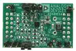
13315-001
Full featured evaluation boards for the ADN8834
Complete TEC controller with integrated 1.5 A TEC driver
Operating voltage range: VIN = 2.7 V to 5.5 V
TEC voltage and current operation monitoring
Independent TEC heating and cooling current-limit settings
Programmable maximum TEC voltage
External synchronization from 1.85 MHz to 3.25 MHz
Input for NTC thermistor connection
Output for TEC module wires
2.5 V reference output
Disable jumper
40 mm × 25 mm WLCSP evaluation board size
45 mm × 25 mm LFCSP evaluation board size
Figure 1. ADN8834CB-EVALZ WLCSP Evaluation Board
DOCUMENTS NEEDED
13315-002
ADN8834 data sheet
Figure 2. ADN8834CP-EVALZ LFCSP Evaluation Board
GENERAL DESCRIPTION
The ADN8834CB-EVALZ and ADN8834CP-EVALZ are
configurable evaluation boards designed to work with various
TEC modules and thermistors. The ADN8834 on the evaluation
board delivers and controls bidirectional current through a TEC
controller using two pairs of the complementary integrated
MOSFETs in an H bridge configuration.
components can be replaced by soldering different value components that match the temperature control loop characteristic
with the thermal load to achieve the required response time and
temperature stability. The cooling and heating TEC current
limits and maximum TEC voltage setting can also be modified
by changing the values of the corresponding components.
The TEC cooling and heating current limits are set to 1.5 A,
and the maximum TEC voltage is programmed to 3 V using
two on-board resistor dividers. The temperature setpoint circuit
is optimized to work with a 10 kΩ NTC thermistor. The on-board
proportional integral differential (PID) compensation network
In addition, the board can be plugged into the ADN8834 base
board, which has adjustable components for the tunable analog
thermal PID network, the temperature setpoint, and maximum
TEC current and TEC voltage limits.
PLEASE SEE THE LAST PAGE FOR AN IMPORTANT
WARNING AND LEGAL TERMS AND CONDITIONS.
Rev. 0 | Page 1 of 16
�UG-858
ADN8834CB-EVALZ/ADN8834CP-EVALZ
TABLE OF CONTENTS
Features .............................................................................................. 1
Cooling and Heating TEC Current Limits ................................4
Documents Needed .......................................................................... 1
PWM Operation Frequency ........................................................4
ADN8834CB-EVALZ and ADN8834CP-EVALZ Evaluation
Boards................................................................................................. 1
Read the TEC Voltage ...................................................................5
General Description ......................................................................... 1
TEC Driver Control ......................................................................5
Revision History ............................................................................... 2
Using the Base Board ........................................................................6
Using the Evaluation Board............................................................. 3
Evaluation Board Schematics and Artwork ...................................7
Board Connection ........................................................................ 3
Ordering Information .................................................................... 14
Maximum TEC Voltage ............................................................... 3
Bill of Materials ........................................................................... 14
Read the TEC Current ..................................................................5
REVISION HISTORY
10/15—Revision 0: Initial Version
Rev. 0 | Page 2 of 16
�ADN8834CB-EVALZ/ADN8834CP-EVALZ
UG-858
USING THE EVALUATION BOARD
where VREF = 2.5 V.
BOARD CONNECTION
Apply a power source to the VIN (ADN8834CB-EVALZ)/VIN+
(ADN8834CP-EVALZ) and GND terminals. Connect the TEC
module to TEC+ and TEC−. Connect the thermistor to the
THERM and AGND terminals. The power source voltage must
be between 2.7 V and 5.5 V, the power supply range of the
ADN8834. Connect the EN/SY pin to VDD and remove the
shunt from the VLIM/SD jumper to enable the controller.
VVLIM_HEATING = VVLIM_COOLING − ISINK_VLIM × RV1||RV2
where ISINK_VLIM = 10 µA.
VTEC_MAX_COOLING = VVLIM_COOLING × AVLIM
where AVLIM = 2 V/V.
VTEC_MAX_HEATING = VVLIM_HEATING × AVLIM
MAXIMUM TEC VOLTAGE
CLK
The maximum TEC cooling voltage is set to 3 V by the values of
RV1 = 6.65 kΩ and RV2 = 10 kΩ.
TEC VOLTAGE
LIMIT AND
INTERNAL
SOFT START
HEATING
To change the setting, modify the value of RV1 using the equations
provided in the Using a Resistor Divider to Set the TEC Voltage
Limit section (for more information, refer to the ADN8834 data
sheet) or by following the recommended values in Table 1.
VREF
DISABLE
RV1
10µA
VLIM/SD
RV2
Calculate the cooling and heating limits using the following
equations:
SW OPEN = VVLIM_COOLING
SW CLOSED = VVLIM_HEATING
13315-003
Using a Resistor Divider to Set the TEC Voltage Limit
Figure 3. Programming the Maximum TEC Voltage
VVLIM_COOLING = VREF × RV2/(RV1 + RV2)
Table 1. Setting the Maximum TEC Voltage (RV2 = 10 kΩ)
VTEC_MAX_COOLING (V)1
4.750
4.500
4.250
4.000
3.750
3.500
3.250
3.000
2.750
2.500
2.250
2.000
1.750
1.500
1.250
1.000
0.750
0.500
0.250
VVLIM_COOLING (V)2
2.375
2.250
2.125
2.000
1.875
1.750
1.625
1.500
1.375
1.250
1.125
1.000
0.875
0.750
0.625
0.500
0.375
0.250
0.125
RV1 (kΩ)3
0.53
1.11
1.76
2.50
3.33
4.29
5.38
6.67
8.18
10.00
12.22
15.00
18.57
23.33
30.00
40.00
56.67
90.00
190.00
VTEC_COOLING (V)4
2.438
2.375
2.313
2.250
2.188
2.125
2.063
2.000
1.938
1.875
1.813
1.750
1.688
1.625
1.563
1.500
1.438
1.375
1.313
RV1||RV2
(kΩ)3
0.5
1.0
1.5
2.0
2.5
3.0
3.5
4.0
4.5
5.0
5.5
6.0
6.5
7.0
7.5
8.0
8.5
9.0
9.5
VVLIM_HEATING (V)5
2.370
2.240
2.110
1.980
1.850
1.720
1.590
1.460
1.330
1.200
1.070
0.940
0.810
0.680
0.550
0.420
0.290
0.160
0.030
VTEC_MAX_COOLING is the maximum target TEC voltage when the ADN8834 operates in cooling mode.
VVLIM_COOLING is the voltage set at the VLIM/SD input pin for cooling.
RV1 is the required value of Resistor R1. RV2 is the required value of Resistor R2.
4
VTEC_COOLING is the voltage at the VTEC output when the TEC voltage reaches the maximum in cooling mode.
5
VVLIM_HEATING is the voltage set at the VLIM/SD input pin for heating.
6
VTEC_MAX_HEATING is the maximum TEC voltage set when the ADN8834 operates in heating mode.
7
VTEC_HEATING is the voltage at the VTEC output when the TEC voltage reaches the maximum in heating mode.
1
2
3
Rev. 0 | Page 3 of 16
VTEC_MAX_HEATING (V)6
4.740
4.480
4.220
3.960
3.700
3.440
3.180
2.920
2.660
2.400
2.140
1.880
1.620
1.360
1.100
0.840
0.580
0.320
0.060
VTEC_HEATING (V)7
0.065
0.130
0.195
0.260
0.325
0.390
0.455
0.520
0.585
0.650
0.715
0.780
0.845
0.910
0.975
1.040
1.105
1.170
1.235
�UG-858
ADN8834CB-EVALZ/ADN8834CP-EVALZ
COOLING AND HEATING TEC CURRENT LIMITS
VDD
The maximum TEC cooling and heating current limits are both
set to 1.5 A by the values of the resistors, RC3 = 210 kΩ and RC4
= 48.7 kΩ. To change the settings, use the equations provided in
the Using a Resistor Divider to Set the TEC Current Limit
section (for more information, refer to the ADN8834 data
sheet) or use the values recommended in Table 3.
40µA
VREF
ITEC
+
ILIM
TEC
CURRENT
LIMIT
SW OPEN = VVLIM_HEATING
SW CLOSED = VVLIM_COOLING
13315-004
RC2
Use the following equations to calculate the maximum TEC
currents:
Figure 4. Programming the TEC Current Cooling and Heating Limits
VILIM_HEATING = VREF × RC2/(RC1 + RC2)
PWM OPERATION FREQUENCY
where VREF = 2.5 V.
The frequency of the PWM TEC driver stage can be configured
at the 3-pin jumper, J1. Apply the external synchronization
clock signal to the middle pin of the jumper. Note that the
middle pin can also be used to shut down the device when it is
pulled below 0.8 V. Therefore, when applying the external clock
signal, ensure that the high level is greater than 2.1 V and the
low level is less than 0.8 V. The combinations of EN/SY pin are
shown in Table 2.
VILIM_COOLING= VILIM_HEATING + ISINK_ILIM × RC1||RC2
where ISINK_ILIM = 40 µA.
VILIM _ COOLING − 1.25 V
RCS
where RCS = 0.525 V/A.
ITEC _ MAX _ HEATING =
–
RC1
Using a Resistor Divider to Set the TEC Current Limit
ITEC _ MAX _ COOLING =
COOLING
1.25 V − VILIM _ HEATING
Table 2. SYNC/EN Pin Settings
RCS
VILIM_HEATING must not exceed 1.2 V and VILIM_COOLING must be
more than 1.3 V to leave proper margins between the heating
and the cooling modes.
SYNC/EN Pin
Low (< 0.8 V)
Open
High (>2.1 V )
External Clock Signal
(High > 2.1 V, Low < 0.8 V)
PWM Operation Frequency
Shutdown
Shutdown
2 MHz
From 1.85 MHz to 3.25 MHz
Table 3. Values of the Resistor Divider for ILIM Settings
ITEC_MAX_COOLING (A)1
1.6
1.5
1.4
1.3
1.2
1.1
1.0
0.9
0.8
0.7
0.6
0.5
0.4
0.3
VILIM_COOLING (V)2
2.090
2.038
1.985
1.933
1.880
1.828
1.775
1.723
1.670
1.618
1.565
1.513
1.460
1.408
ITEC_MAX_HEATING (A)3
−1.6
−1.5
−1.4
−1.3
−1.2
−1.1
−1.0
−0.9
−0.8
−0.7
−0.6
−0.5
−0.4
−0.3
VILIM_HEATING (V)4
0.410
0.463
0.515
0.568
0.620
0.673
0.725
0.778
0.830
0.883
0.935
0.988
1.040
1.093
ITEC_MAX_COOLING is the maximum target TEC current when the ADN8834 operates in cooling mode.
VILIM_COOLING is the voltage set at the ILIM pin when the ADN8834 operates in cooling mode.
3
ITEC_MAX_HEATING is the maximum target TEC current when the ADN8834 operates in heating mode.
4
VILIM_HEATING is the voltage set at the ILIM pin when the ADN8834 operates in heating mode.
5
RC1 is the required value of Resistor R3. RC2 is the required value of Resistor R4.
1
2
Rev. 0 | Page 4 of 16
RC1 (kΩ)5
256.1
212.8
178.4
150.3
127.0
107.3
90.5
76.0
63.3
52.1
42.1
33.2
25.2
18.0
RC2 (kΩ)5
50.2
48.3
46.3
44.1
41.9
39.5
37.0
34.3
31.4
28.4
25.2
21.7
18.0
14.0
RC1||RC2 (kΩ)5
42.000
39.375
36.750
34.125
31.500
28.875
26.250
23.625
21.000
18.375
15.750
13.125
10.500
7.875
�ADN8834CB-EVALZ/ADN8834CP-EVALZ
UG-858
READ THE TEC VOLTAGE
TEC DRIVER CONTROL
The voltage on the VTEC output pin is proportional to the
voltage across the TEC and is measured at Connector J5/Pin 1
(ADN8834CB-EVALZ) or J6/Pin 11 (ADN8834CP-EVALZ). The
relationship between the voltage on the VTEC output and the
voltage across the TEC is as follows:
The TEC driver has a linear driver LDR and a PWM driver with
an SW output and a voltage feedback input pin, SFB. It is
controlled by the voltage signal at the OUT2 pin. The equations
for the linear and PWM driver outputs, respectively, are as
follows:
VTEC = VLDR − VSFB = 4 × (VVTEC − 0.5 × VREF)
where:
VTEC is the voltage across the TEC.
VLDR is the voltage measured at the LDR pin.
VSFB is the voltage measured at the SFB pin.
VVTEC is the voltage measured at the VTEC pin.
VREF is the reference voltage, 2.5 V.
(1)
VSFB = VLDR + 5 (VOUT2 − 1.25 V)
(2)
where:
VOUT2 is the voltage at the OUT2 pin.
VB is determined by voltage at the VDD pin as
READ THE TEC CURRENT
The voltage on the ITEC output pin is proportional to the TEC
current, and is measured at Connector J5/Pin 2 (ADN8834CBEVALZ) or J6/Pin 12 (ADN8834CP-EVALZ). Calculate the TEC
current from the ITEC pin voltage as follows:
ITEC =
VLDR = VB − 40 (VOUT2 − 1.25 V)
VITEC − 0.5 × VREF
RCS
where:
ITEC is the TEC current; defined as the current flowing into the
TEC positive terminal, TEC+, and out of the TEC negative
terminal, TEC−.
VITEC is the voltage measured at the ITEC pin.
RCS is the current sense gain, 0.525 V/A.
VREF is the reference voltage, 2.5 V.
VB = 1.5 V (VVDD < 4.0 V)
(3)
VB = 2.5 V (VVDD > 4.0 V)
(4)
The VLDR and VSFB voltages are limited by the power supply
voltage with the upper limit of VVDD and the lower limit of 0 V.
The voltage at the OUT2 pin is determined by the compensation
amplifier with the PID network. This amplifier receives the
temperature setpoint voltage at the IN2P input and the thermistor
voltage at the IN2N pin fed by the OUT1 pin of the error amplifier.
If the digital temperature control loop is used, configure the
compensation amplifier as a unity-gain follower by connecting
the OUT2 pin to IN2N, and then apply the control signal from
a DAC to the IN2P input. Thus, the OUT2 pin voltage is equal
to the DAC voltage at the IN2P pin, and the TEC driver outputs
follow Equation 1 and Equation 2.
Rev. 0 | Page 5 of 16
�UG-858
ADN8834CB-EVALZ/ADN8834CP-EVALZ
USING THE BASE BOARD
Table 4. Configuration Components to Be Removed from
ADN8834CB-EVALZ or ADN8834CP-EVALZ Board
Component
R1
R3
R4
R10
C7
R13
R16
R17
R11
C8
C6
R9
R8
R12
13315-005
The ADN8834 base board, which is available upon request,
allows the user to tune the PID components in analog thermal
control loop because it has a set of selectable R and C values. In
addition, it offers adjustable components that allow the user to
change the maximum TEC voltage and cooling and heating
current limits. The temperature setpoint can be also changed
manually. Connect a ADN8834CB-EVALZ or ADN8834CPEVALZ board to the base board as the daughter card. To avoid
duplication, remove several configuration components from the
daughter card before connecting it into the ADN8834 base
board (see Table 4).
Figure 5. ADN8834 Base Board
Rev. 0 | Page 6 of 16
Value
6.65 kΩ
210 kΩ
48.7 kΩ
165 kΩ
10 µF
1.87 MΩ
20 kΩ
20 kΩ
1.87 MΩ
1.5 µF
0.01 µF
80.6 kΩ
7.68 kΩ
17.8 kΩ
Function
Voltage limit (VLIM)
Current limit (ILIM)
ILIM
PID compensation amplifier
PID compensation amplifier
PID compensation amplifier
Temperature setpoint (TEMPSET)
TEMPSET
PID compensation amplifier
PID compensation amplifier
PID compensation amplifier
Thermistor amplifier
Thermistor amplifier
Thermistor amplifier
�CON12
J4
1
2
3
4
5
6
7
8
9
10
11
12
CONT
ILIM
VLIM/SD
AGND
VREF
TEMPOUT
TEMPSET
CMIN
TPR123
CRDR
CIRP
GND_THERM
R3
10
R5
210K
R4
20K
17.8K
TP9AGND
R14
R12
R8
7.68K
TPR123
C4
0.1UF
TP21THRMSTR
VREF
VIN+
3
2
1
THERMISTOR
J1EN/SY
1
TP22ILIM
VREF
C3
0.1UF
R20
0
TP4
48.7K
6.65K
1
IN1P
IN1M
VREF
R15
20K
10K
R9
TEMPSET
AGND
E4
E5
D5
VDD
VREF
D4
C5
B5
EN/SY
ILIM
VLIM/SD
R2
OUT1
80.6K
AGND
VREF
VDD
EN/SY
ILIM
VLIM/SD
U1
VTEC
ITEC
ADN8834ACBZ
R27
0
R17
R16
20K
20K
1.87M
10UF
C7
0
R22
TEMPOUT
R13
165K
VREF
R10
0
R21
C4
OUT2
OUT2
B4
IN2N
IN2N
A5
IN2P
IN2P
A4
IN1P
IN1P
D3
VTEC
C3
ITEC
E3
SFB
IN1N
B3
IN1N
OUT1
A3
OUT1
1
0
C6
0.01U
C8
NP
L1
1.5U
0
1
NP
R26
R25
0
1
CONT
IN2M
AGND
TP1
TP19OUT2
CIRP
TEC(-)
TEC(+)
TP2
VIN(+)
TP13
VIN+
1UH
C110UF
OUT2
C5
0.1UF
C2
10UF
CMIN
R24
R28
CRDR
A1
A2
B2
B1
C2
C1
D2
D1
E1
E2
TP17IN2P
R18
IN2P
IN2M
499K
TP23IN2M
R11
1.87M
R23
PGNDL
PGNDL
LDR
LDR
PVIN
PVIN
SW
SW
PGNDS
PGNDS
49.9
R29
1
R1
1
1
2
1
Rev. 0 | Page 7 of 16
1
Figure 6. ADN8834CB-EVALZ WLCSP Evaluation Board Schematic
1
AGND
GND
TP15
TP11
C9
0.1UF
1
VIN+
GND_THERM
THERMISTOR
TEC(+)
GND
VIN+
VTEC
ITEC
TEC(-)
1
J2VLIM/SD
+
CON12
J5
GND
C10
100uF
1
2
3
4
5
6
7
8
9
10
11
12
ADN8834CB-EVALZ/ADN8834CP-EVALZ
UG-858
EVALUATION BOARD SCHEMATICS AND ARTWORK
13315-006
�Rev. 0 | Page 8 of 16
GND_THERM
1
2
3
4
5
6
7
8
9
10
11
12
THERMISTOR
CON12
J4
VREF
TP9
AGND
R14
20K
17.8K
7.68K
0
R20
210K
R5
10
R15
20K
IN1P
IN1M
48.7K
R4
10K
6.65K
R3
VIN+
R12
R8
TP21THERM
TPR123
TEMPOUT
TEMPSET
CMIN
TPR123
CDRD
CIRP
TEMPGOOD
CONT
ILIM
VLIM/SD
AGND
VREF
VREF
R2
R1
R9
TEMPSET
C4
0.1UF
OUT1
80.6K
1
C3
0.1UF
TP4VREF
1
VLIM/SD
R27
6
5
0
VREF
VDD
ILIM
VLIM/SD
OUT2
IN2N
J1EN/SY
IN1P
R17
R16
20K
20K
1.87M
10UF
C7
0
R22
TEMPOUT
R13
165K
VREF
R10
OUT1
TP20
0
R21
VREF
VDD
4
2
3
OUT2
ILIM
1
IN2N
U1
PAD
1
2
3
1
2
IN2P
24
IN2P
7
PD
23
IN1P
IN1N
8
1
TP18
IN2M
R23
499K
TP17
IN2P
R18
IN2P
0
C6
CDRD
VTEC
R111.87M
IN2M
1
ADN8834ACPZ
EN/SY
EN/SY
AGND
22
IN1N
OUT1
OUT1
21
VTEC
9
SFB
10
19
PGNDL
20
TMPGD
11
PGNDS
NP
R28
1
1.5UF
0.01UF
C8
0
CMIN
R24
ITEC
SW
PVINS
PVINL
LDR
PGNDL
PGNDS
12
ITEC
TEMPGOOD
OUT2
TP19
NP
R26
R25
0
C2
10UF
0.1UF
OUT2
CIRP
49.9
R19
13
14
15
16
17
18
C11
TP2
1UH
L1
0.1UF
C5
IN2M
CONT
1
TEC-
C1
NP
TP11
TP13
1
1
J2VLIM/SD
1
Figure 7. ADN8834CP-EVALZ LFCSP Evaluation Board Schematic
1
VIN+
C12
10UF
VIN+
TEC(-)
TEC(+)
TP1
AGND
1
AGND
VTEC
ITEC
TEC(-)
GND
VIN+
GND_THERM
THERMISTOR
TEC(+)
GND
VIN+
CON12
J6
TP15
C9
0.1UF
1
2
3
4
5
6
7
8
9
10
11
12
1
+
GND
C10
100uF
UG-858
ADN8834CB-EVALZ/ADN8834CP-EVALZ
13315-007
�VREF
TP5
TP4
AGND
1
TEMPOUT
20K
W3
VREF
W1
20K
J2
CONT
1
2
1
TEMPSET
TEMPOUT
10K
Figure 8. ADN8834 Base Board Schematic
TP10
1
2
100K
W7
CD5 10UF
SW2
SDA05H1SBD
AGND
J11
VLIM/SD
1UF
CD2
CD1 .47UF
2.2uF
CD3
W6
500K
TEMPOUT
TPR123
TEMPSET
CD4 4.7UF
W5
TP15
200K
R2
TPR123
W4
200K
10K
R1
TP19
1
1
1
1
CDRD
1
SW3
ILIM
SDA05H1SBD
SW6
SDA05H1SBD
TP16
1
A2
TEMPSET
RD1
12K
RI1
61.9K
A12
C1
B11
RD2 24K
249K
RD3 49.9K
RI3
D1
ITEC
C12
499K
RD4 100K
RI4
VIN+
VTEC
200K
RD5
RI5
1MEG
ADN8834 ADN8833 DAUGHTER
LG T67K-H2K1-24-Z (green)
J4_VREF
J6_GND_THERM
J5_GND_THERM
J5_THERMISTER
J6_THERMISTER
J4_TEMPSET
J4_TEMPGOOD
J4_TEMPOUT
RI6 1K
TEMPGOOD
RI2 124K
VREF
GND_THERM
B12
C2
A7
TEMPGOOD
THERMISTOR
A1
TEMPOUT
U1
ILIM
A9
J4_ILIM
A4
TPR123
J4_TPR123
A5
J4_CDRD
CDRD
J5_ITEC
A10
J4_VLIM/SD
VLIM/SD
J4_CONT
A8
CONT
J4_CMIN
A3
CMIN
J4_AGND
A11
CMIN
TP3
C8
J4_CIRP
A6
CIRP
B2
J5_ITEC
B1
J5_VTEC
C11
J6_VTEC
B5
J5_VIN+
B6
J5_VIN+
C5
J6_VIN+
J6_GND
C6
J6_VIN+
J6_GND
C7
J5_GND
B8
C10
C9
C4
C3
B4
B3
B10
TP25
SDA05H1SBD
SW4
TEMPOUT
J6_TEC(-)
J6_TEC(-)
J6_TEC(+)
J6_TEC(+)
J5_TEC(-)
J5_TEC(-)
J5_TEC(+)
B9
VTEC
ITEC
J5_TEC(+)
J5_GND
B7
1
1
TP2
TP12
TEC(-)
TEC(+)
RP1
61.9K
1
TP24
CD
TP17
NP
RP2 124K
NP
RI
RP3 249K
RD NP
TP14
1
CMIN
VREF
TP18
0.01UF
RP4 499K
RP NP
CF
AGND
C17
0.1UF
NP
RP5 1MEG
CI
TP20
1
TP6
TPR123
Short = gnd:gnd_signal
1
1
1
CDRD
1
CIRP
Rev. 0 | Page 9 of 16
W2
20K
GND
C16
150uF
VIN+
CONT
CIRP
TP8
C13
TP22
TP21
TEC(+)
TEC(-)
GND
VIN+
1
TP23
0.47UF
1UF
C11
0.047uF
C12 0.1uF
0.22uF
C14
C15
1
2
1
2
1
2
GND_THERM
THERMISTOR
THERMISTOR
GND_THERM
TP13
1
1
1 1
TP1
SDA05H1SBD
SW5
LUMBERGKRM2
J10
LUMBERGKRM2
J9
LUMBERGKRM2
J8
CONT
ADN8834CB-EVALZ/ADN8834CP-EVALZ
UG-858
13315-008
�13315-011
ADN8834CB-EVALZ/ADN8834CP-EVALZ
13315-009
UG-858
13315-010
13315-012
Figure 11. ADN8834CB-EVALZ Evaluation Board Second Layer
Figure 9. ADN8834CB-EVALZ Evaluation Board Top Layer
Figure 12. ADN8834CB-EVALZ Evaluation Board Bottom Layer
Figure 10. ADN8834CB-EVALZ Evaluation Board Third Layer
Rev. 0 | Page 10 of 16
�UG-858
13315-013
ADN8834CB-EVALZ/ADN8834CP-EVALZ
13315-014
Figure 13. ADN8834CP-EVALZ Evaluation Board Top Layer
13315-015
Figure 14. ADN8834CP-EVALZ Evaluation Board Second Layer
13315-016
Figure 15. ADN8834CP-EVALZ Evaluation Board Third Layer
Figure 16. ADN8834CP-EVALZ Evaluation Board Bottom Layer
Rev. 0 | Page 11 of 16
�13315-017
ADN8834CB-EVALZ/ADN8834CP-EVALZ
Figure 17. ADN8834 Base Board Top Layer
13315-018
UG-858
Figure 18. ADN8834 Base Board Layer 2
Rev. 0 | Page 12 of 16
�UG-858
13315-019
ADN8834CB-EVALZ/ADN8834CP-EVALZ
13315-020
Figure 19. ADN8834 Base Board Layer 3
Figure 20. ADN8834 Base Board Bottom Layer
Rev. 0 | Page 13 of 16
�UG-858
ADN8834CB-EVALZ/ADN8834CP-EVALZ
ORDERING INFORMATION
BILL OF MATERIALS
Table 5. ADN8834CB-EVALZ WLCSP Evaluation Board
Quantity
3
5
2
1
1
1
2
1
1
1
1
1
1
1
1
1
1
1
1
4
1
7
11
1
Reference
C1, C2, C8
C3, C4, C5, C9, C11
C6, C7
C10
J1
J2
J4, J5
L1
R1
R2
R3
R4
R5
R8
R9
R12
R10
R11
R13
R14, R15, R16, R17
R18
R20, R21, R22, R23, R24,
R25, R27
TP1, TP4, TP9, TP11,
TP15, TP17, TP18, TP19,
TP20, TP21, TP22
U1
Description
Ceramic capacitor, 10 µF, 10 V, 10%, X7R, 0805
Ceramic capacitor, 0.1 µF, 10 V, 10%, X7R, 0603
Ceramic capacitor, 0.01 µF, 50 V, 10%, X7R, 0603
Tantalum capacitor, 100 µF, 6.3 V, 20%, 1411
Jumper, 3-pin
Jumper, 2-pin
Connector, double row, male, 12-pin
Inductor, 1 µH
Resistor, 6.65 kΩ, 1/10 W, 1%, 0603, SMD
Resistor, 10 kΩ, 1/10 W, 1%, 0603, SMD
Resistor, 210 kΩ, 1/10 W, 1%, 0603, SMD
Resistor, 48.7 kΩ, 1/10 W, 1%, 0603, SMD
Resistor, 10.0 Ω, 1/10 W, 1%, 0603, SMD
Resistor, 7.68 kΩ, 1/10 W, 1%, 0603, SMD
Resistor, 80.6 kΩ, 1/10 W, 1%, 0603, SMD
Resistor, 17.8 kΩ, 1/10 W, 1%, 0603, SMD
Resistor, 374 kΩ, 1/10 W, 1%, 0603, SMD
Resistor, 100 kΩ, 1/10 W, 1%, 0603, SMD
Resistor, 64.9 kΩ, 1/10 W, 1%, 0603, SMD
Resistor, 20.0 kΩ, 1/10 W, 1%, 0603, SMD
Resistor, 499 kΩ, 1/10 W, 1%, 0603, SMD
Resistor, 0.0 Ω, 1/10 W, 0603, SMD
Manufacturer
Taiyo Yuden
Kemet
Kemet
Vishay
Samtec
Samtec
Samtec
TOKO
Vishay
Vishay
Vishay
Vishay
Vishay
Vishay
Vishay
Vishay
Vishay
Vishay
Vishay
Vishay
Vishay
Vishay
Part Number
LMK212B7106KG-TD
C0603C104K8RACTU
C0603C103K5RACTU
293D107X06R3B2T
TSW-103-08-G-S
TSW-103-08-G-S
TSW-112-08-G-D
1286AS-H-1R0M
CRCW06036K65FKEA
ERJ-3EKF1002V
CRCW0603210KFKEA
CRCW060348K7FKEA
CRCW060310R0FKEA
CRCW06037K68FKEA
CRCW060380K6FKEA
CRCW060317K8FKEA
CRCW0603165KFKEA
CRCW0603100KFKEA
CRCW060364K9FKEA
CRCW060320K0FKEA
ERJ-3EKF4993V
ERJ-3GEY0R00V
Test point
Samtec
TSW-103-08-G-S
Ultracompact, 1.5 A, TEC controller, WLCSP
package
Analog Devices,
Inc.
ADN8834ACBZ-R7
Table 6. ADN8834CP-EVALZ LFCSP Evaluation Board
Quantity
3
5
2
1
1
1
2
1
1
1
1
1
1
1
1
1
1
Reference
C2, C8, C12
C3, C4, C5, C9, C11
C6, C7
C10
J1
J2
J4, J6
L1
R1
R2
R3
R4
R5
R8
R9
R12
R10
Description
Ceramic capacitor, 10 µF, 10 V, 10%, X7R 0805
Ceramic capacitor, 0.1 µF, 10 V, 10%, X7R 0603
Ceramic capacitor, 0.01 µF, 50 V, 10%, X7R 0603
Tantalum capacitor, 100 µF, 6.3 V, 20%, 1411
Jumper, 3-pin
Jumper, 2-pin
Connector, double row, male, 12-pin
Inductor, 1 µH
Resistor, 6.65 kΩ, 1/10 W, 1%, 0603, SMD
Resistor, 10 kΩ, 1/10 W, 1%, 0603, SMD
Resistor, 210 kΩ, 1/10 W, 1%, 0603, SMD
Resistor, 48.7 kΩ, 1/10 W, 1%, 0603, SMD
Resistor, 10.0 Ω, 1/10 W, 1%, 0603, SMD
Resistor, 7.68 kΩ, 1/10 W, 1%, 0603, SMD
Resistor, 80.6 kΩ 1/10 W, 1%, 0603, SMD
Resistor, 17.8 kΩ, 1/10 W, 1%, 0603, SMD
Resistor, 374 kΩ, 1/10 W, 1%, 0603, SMD
Rev. 0 | Page 14 of 16
Manufacturer
Taiyo Yuden
Kemet
Kemet
Vishay
Samtec
Samtec
Samtec
Coilcraft
Vishay
Vishay
Vishay
Vishay
Vishay
Vishay
Vishay
Vishay
Vishay
Part Number
LMK212B7106KG-TD
C0603C104K8RACTU
C0603C103K5RACTU
293D107X06R3B2T
TSW-103-08-G-S
TSW-103-08-G-S
TSW-112-08-G-D
XFL3012-102ME
CRCW06036K65FKEA
ERJ-3EKF1002V
CRCW0603210KFKEA
CRCW060348K7FKEA
CRCW060310R0FKEA
CRCW06037K68FKEA
CRCW060380K6FKEA
CRCW060317K8FKEA
CRCW0603165KFKEA
�ADN8834CB-EVALZ/ADN8834CP-EVALZ
Quantity
1
1
4
1
1
7
10
2
1
Reference
R11
R13
R14, R15, R16, R17
R18
R19
R20, R21, R22, R23, R24, R25,
R27
TP1, TP4, TP9, TP13, TP15,
TP17, TP18, TP19, TP20, TP21
TP2, TP11
U1
UG-858
Description
Resistor, 562 kΩ, 1/10 W, 1%, 0603, SMD
Resistor, 64.9 kΩ, 1/10 W, 1%, 0603, SMD
Resistor, 20.0 kΩ, 1/10 W, 1%, 0603, SMD
Resistor, 499 kΩ, 1/10 W, 1%, 0603, SMD
Resistor, 49.9 Ω, 1/10 W, 1%, 0603, SMD
Resistor, 0.0 Ω, 1/10 W, 0603, SMD
Manufacturer
Vishay
Vishay
Vishay
Vishay
Vishay
Vishay
Part Number
CRCW06031M87FKEA
CRCW060364K9FKEA
CRCW060320K0FKEA
ERJ-3EKF4993V
CRCW060349R9FKEA
ERJ-3GEY0R00V
Test point
Keystone
5010
Connector
Ultracompact, 1.5 A, TEC controller, LFCSP
package
Mill-Max
Analog Devices
3102-2-00-21-00-08-0
ADN8834ACPZ-R7
Table 7. ADN8834 Base Board
Quantity
2
2
1
1
1
1
1
2
1
1
1
2
3
1
1
1
1
1
2
2
2
2
2
1
2
5
18
1
3
2
1
1
1
Reference
CD1, C14
CD2, C15
CD3
CD4
CD5
CF
C11
C12, C17
C13
C16
D1
J2, J11
J8, J9, J10
RD1
RD2
RD3
RD4
RD5
RP1, RI1
RP2, RI2
RP3, RI3
RP4, RI4
RP5, RI5
RI6
R1, R2
SW2, SW3, SW4, SW5, SW6
TP1, TP2, TP3, TP4, TP5, TP6,
TP8, TP10, TP12, TP13, TP14,
TP15, TP16, TP17, TP18, TP19,
TP20, TP21
U1
W1, W2, W3
W4, W5
W6
W7
Description
Ceramic capacitor, 0.47 µF, 16 V, 10%, X5R, 0603
Ceramic capacitor, 1 µF, 16 V, 10%, X5R, 0603
Ceramic capacitor, 2.2 µF, 16 V, 10%, X5R, 0603
Ceramic capacitor, 4.7 µF, 6.3 V, 10%, X5R, 0603
Ceramic capacitor, 10 µF, 6.3 V, 20%, X5R, 0603
Ceramic capacitor, 0.01 µF, 50 V, 10%, X7R, 0603
Ceramic capacitor, 0.047 µF, 6.3 V, 10%, X5R, 0603
Ceramic capacitor, 0.1 µF, 50 V, 10%, X7R, 0603
Ceramic capacitor, 0.22 µF, 6.3 V, 10%, X5R, 0603
Tantalum capacitor, 150 µF, 6.3 V, 20%, 2917
LED, green, 570 nm, clear, 2-PLCC
Jumper, 2-pin
Connector, PCB terminal, black, 2-pin
Resistor, 12 kΩ, 1/10 W, 1%, 0603, SMD
Resistor, 24.3 kΩ, 1/10 W, 1%, 0603, SMD
Resistor, 49.9 kΩ, 1/10 W, 1%, 0603, SMD
Resistor, 100 kΩ, 1/10 W, 1%, 0603, SMD
Resistor, 200 kΩ, 1/10 W, 1%, 0603, SMD
Resistor, 61.9 kΩ, 1/10 W, 1%, 0603, SMD
Resistor, 124 kΩ, 1/10 W, 1%, 0603, SMD
Resistor, 249 kΩ, 1/10 W, 1%, 0603, SMD
Resistor, 499 kΩ, 1/10 W, 1%, 0603, SMD
Resistor, 1 MΩ, 1/10 W, 1%, 0603, SMD
Resistor, 1 kΩ, 1/10 W, 1%, 0603, SMD
Resistor, 10 kΩ, 1/10 W, 1%, 0603, SMD
Switch, low profile DIP, top slide, 5-position
Test point
Manufacturer
TDK
Murata
Murata
Murata
Panasonic
Kemet
Murata
AVX
TDK
Sanyo
OSRAM
Samtec
On Shore
Vishay
Vishay
Panasonic
Vishay
Panasonic
Vishay
Vishay
Panasonic
Panasonic
Vishay
Panasonic
Panasonic
C&K
Keystone
Part Number
C1608X5R1C474K080AA
GRM188R61C105KA
GRM188R61C225KE
GRM188R60J475KE19D
ECJ-1VB0J106M
C0603C103K5RACTU
GRM033R60J473KE19D
06035C104KAT2A
C0603X5R0J224K030BB
6TPE150MI
LG T67K-H2K1-24-Z
TSW-150-07-G-S
OSTVN02A150
CRCW060312K0FKEA
CRCW060324K3FKEA
ERJ-3EKF4992V
CRCW0603100KFKEA
ERJ-3EKF2003V
CRCW060361K9FKEA
CRCW0603124KFKEA
ERJ-3EKF2493V
ERJ-3EKF4993V
CRCW06031M00FKEA
ERJ-6ENF4123V
ERJ-3EKF1002V
SDA05H1SBD
5010
Connector1
Trimmer, 20 kΩ, 0.25 W, SMD
Trimmer, 200 kΩ, 0.25 W, SMD
Trimmer, 500 kΩ, 0.25 W, SMD
Trimmer, 100 kΩ, 0.25 W, SMD
Samtec
Murata
Murata
Murata
Murata
SSW-106-01-G-D
PVG5A203C03R00
PVG5A204C03R00
PVG5A504C03R00
PVG5A104C03R01
U1 has a reserved area to plug in the daughter board. The silkscreen mark includes three 12-pin female connectors and several other components.
Rev. 0 | Page 15 of 16
�UG-858
ADN8834CB-EVALZ/ADN8834CP-EVALZ
NOTES
ESD Caution
ESD (electrostatic discharge) sensitive device. Charged devices and circuit boards can discharge without detection. Although this product features patented or proprietary protection
circuitry, damage may occur on devices subjected to high energy ESD. Therefore, proper ESD precautions should be taken to avoid performance degradation or loss of functionality.
Legal Terms and Conditions
By using the evaluation board discussed herein (together with any tools, components documentation or support materials, the “Evaluation Board”), you are agreeing to be bound by the terms and conditions
set forth below (“Agreement”) unless you have purchased the Evaluation Board, in which case the Analog Devices Standard Terms and Conditions of Sale shall govern. Do not use the Evaluation Board until you
have read and agreed to the Agreement. Your use of the Evaluation Board shall signify your acceptance of the Agreement. This Agreement is made by and between you (“Customer”) and Analog Devices, Inc.
(“ADI”), with its principal place of business at One Technology Way, Norwood, MA 02062, USA. Subject to the terms and conditions of the Agreement, ADI hereby grants to Customer a free, limited, personal,
temporary, non-exclusive, non-sublicensable, non-transferable license to use the Evaluation Board FOR EVALUATION PURPOSES ONLY. Customer understands and agrees that the Evaluation Board is provided
for the sole and exclusive purpose referenced above, and agrees not to use the Evaluation Board for any other purpose. Furthermore, the license granted is expressly made subject to the following additional
limitations: Customer shall not (i) rent, lease, display, sell, transfer, assign, sublicense, or distribute the Evaluation Board; and (ii) permit any Third Party to access the Evaluation Board. As used herein, the term
“Third Party” includes any entity other than ADI, Customer, their employees, affiliates and in-house consultants. The Evaluation Board is NOT sold to Customer; all rights not expressly granted herein, including
ownership of the Evaluation Board, are reserved by ADI. CONFIDENTIALITY. This Agreement and the Evaluation Board shall all be considered the confidential and proprietary information of ADI. Customer may
not disclose or transfer any portion of the Evaluation Board to any other party for any reason. Upon discontinuation of use of the Evaluation Board or termination of this Agreement, Customer agrees to
promptly return the Evaluation Board to ADI. ADDITIONAL RESTRICTIONS. Customer may not disassemble, decompile or reverse engineer chips on the Evaluation Board. Customer shall inform ADI of any
occurred damages or any modifications or alterations it makes to the Evaluation Board, including but not limited to soldering or any other activity that affects the material content of the Evaluation Board.
Modifications to the Evaluation Board must comply with applicable law, including but not limited to the RoHS Directive. TERMINATION. ADI may terminate this Agreement at any time upon giving written notice
to Customer. Customer agrees to return to ADI the Evaluation Board at that time. LIMITATION OF LIABILITY. THE EVALUATION BOARD PROVIDED HEREUNDER IS PROVIDED “AS IS” AND ADI MAKES NO
WARRANTIES OR REPRESENTATIONS OF ANY KIND WITH RESPECT TO IT. ADI SPECIFICALLY DISCLAIMS ANY REPRESENTATIONS, ENDORSEMENTS, GUARANTEES, OR WARRANTIES, EXPRESS OR IMPLIED, RELATED
TO THE EVALUATION BOARD INCLUDING, BUT NOT LIMITED TO, THE IMPLIED WARRANTY OF MERCHANTABILITY, TITLE, FITNESS FOR A PARTICULAR PURPOSE OR NONINFRINGEMENT OF INTELLECTUAL
PROPERTY RIGHTS. IN NO EVENT WILL ADI AND ITS LICENSORS BE LIABLE FOR ANY INCIDENTAL, SPECIAL, INDIRECT, OR CONSEQUENTIAL DAMAGES RESULTING FROM CUSTOMER’S POSSESSION OR USE OF
THE EVALUATION BOARD, INCLUDING BUT NOT LIMITED TO LOST PROFITS, DELAY COSTS, LABOR COSTS OR LOSS OF GOODWILL. ADI’S TOTAL LIABILITY FROM ANY AND ALL CAUSES SHALL BE LIMITED TO THE
AMOUNT OF ONE HUNDRED US DOLLARS ($100.00). EXPORT. Customer agrees that it will not directly or indirectly export the Evaluation Board to another country, and that it will comply with all applicable
United States federal laws and regulations relating to exports. GOVERNING LAW. This Agreement shall be governed by and construed in accordance with the substantive laws of the Commonwealth of
Massachusetts (excluding conflict of law rules). Any legal action regarding this Agreement will be heard in the state or federal courts having jurisdiction in Suffolk County, Massachusetts, and Customer hereby
submits to the personal jurisdiction and venue of such courts. The United Nations Convention on Contracts for the International Sale of Goods shall not apply to this Agreement and is expressly disclaimed.
©2015 Analog Devices, Inc. All rights reserved. Trademarks and
registered trademarks are the property of their respective owners.
UG132423-0-10/15(0)
Rev. 0 | Page 16 of 16
�


 工商网监
湘ICP备2023018690号
工商网监
湘ICP备2023018690号
