ADP1046A 100 Watt Evaluation Kit
ADP1046A-100-EVALZ
PRD1386
FEATURES
100W Full Bridge Topology (adjustable to full bridge phase shifted topology)
Advanced Voltage Mode Control with Integrated Volt-Second Balance
I2C Serial Interface to PC
Software GUI
Programmable Digital Filters
7 PWM Outputs Including Auxiliary PWM
Digital Trimming
OrFET Control for Hot Swap and Redundancy
Current, Voltage, and Temperature Sense through GUI
Calibration and Trimming
Analog/Digital Current Sharing
Line Voltage Feed Forward
CAUTION
This evaluation board uses high voltages and currents. Extreme caution must be taken especially on the primary
side, to ensure safety for the user. It is strongly advised to power down the evaluation board when not in use. A
current limited power supply is recommended as the input has no fuse present on the board.
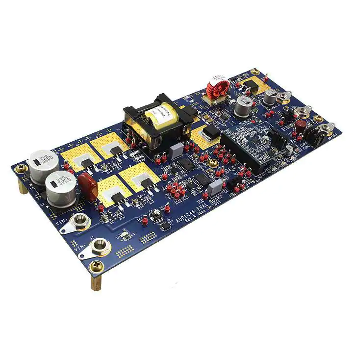
ADP1046A EVALUATION BOARD OVERVIEW
This evaluation board features the ADP1046A in a switching power supply application. With the evaluation board and
software, the ADP1046A can be interfaced with any PC running Windows 2000/XP/Vista/NT/7 via the computer's USB port.
The software allows control and monitoring of the ADP1046A internal registers. The board is set up for the ADP1046A to act
as an isolated switching power supply with a rated load of 12V/8A from an input voltage ranging from a 36 to 60VDC.
EVALUATION SYSTEM CONTENTS
The evaluation system package contains the following items:
• One ADP1046A evaluation board and one daughter card.
The USB/I2C dongle for serial communication and software CD needs to be ordered separately.
Order code: ADP-I2C-USB-Z
Rev. 1.3
Reference designs are as supplied “as is” and without warranties of any kind, express, implied, or
statutory including, but not limited to, any implied warranty of merchantability or fitness for a
particular purpose. No license is granted by implication or otherwise under any patents or other
intellectual property by application or use of reference designs. Information furnished by Analog
Devices is believed to be accurate and reliable. However, no responsibility is assumed by Analog
Devices for its use, nor for any infringements of patents or other rights of third parties that may
result from its use. Analog Devices reserves the right to change devices or specifications at any
time without notice. Trademarks and registered trademarks are the property of their respective
owners. Reference designs are not authorized to be used in life support devices or systems.
One Technology Way, P.O. Box 9106, Norwood, MA 02062-9106, U.S.A.
Tel: 781.329.4700
www.analog.com
Fax: 781.461.3113
©2009 Analog Devices, Inc. All rights reserved.
�ADP1046A 100Watt
Evaluation board
PRD1386
TABLE OF CONTENTS
Features ....................................................................................................................................................................................... 1
Caution ......................................................................................................................................................................................... 1
ADP1046A Evaluation Board Overview........................................................................................................................................ 1
Evaluation System Contents ........................................................................................................................................................ 1
Topology and Circuit Description .................................................................................................................................................. 4
Connectors ................................................................................................................................................................................... 4
Setting Files and EEPROM ...................................................................................................................................................... 6
Board Evaluation .......................................................................................................................................................................... 7
Equipment ................................................................................................................................................................................ 7
Setup ........................................................................................................................................................................................ 8
ADP1046A Programming Software......................................................................................................................................... 10
Flags Settings Configurations ................................................................................................................................................. 11
General Settings and Softstart ................................................................................................................................................... 12
PWM AND SR Settings .............................................................................................................................................................. 15
CS1 OR Input Current Setting .................................................................................................................................................... 16
CS2 OR Output Current Setting ................................................................................................................................................. 20
Light Load Mode ..................................................................................................................................................................... 22
Output Voltage Settings .............................................................................................................................................................. 24
Digital Filter Settings and Transient Analysis .............................................................................................................................. 27
OrFET Settings........................................................................................................................................................................... 31
Full Bridge Phase Shifted Mode ................................................................................................................................................. 35
Line Voltage Feedforward .......................................................................................................................................................... 37
Appendix I – Schematic (Main Board) ........................................................................................................................................ 39
Appendix II – Schematic (Daughter Card) .................................................................................................................................. 40
Appendix III – Layout (Main Board) ............................................................................................................................................ 41
Appendix IV – Layout (Daughter Card) ...................................................................................................................................... 44
Appendix V - Transformer Specification ..................................................................................................................................... 47
Appendix VI - Output Inductor Specification ............................................................................................................................... 49
Appendix VII - Thermal Performance ......................................................................................................................................... 50
Appendix VII - Thermal Performance ......................................................................................................................................... 50
Appendix VIII – Efficiency and Voltage Regulation ..................................................................................................................... 52
Notes .......................................................................................................................................................................................... 55
REVISION HISTORY
10/03/2011—Revision 1.0: NSD
07/15/2012—Revision 2.0: SPM
08/03/2012—Revision 2.1: SPM
Rev. 1.3 | Page 2 of 55
�ADP1046A 100Watt
Evaluation board
PRD1386
Figure 1 - Simplified block diagram
DEMO BOARD SPECIFICATIONS
Specification
VIN
MIN
TYP
MAX
Units
36
48
60
V
VOUT
IOUT
TAMBIENT
12
Switching frequency
V
0.0
8.0
10
A
0
30
65
ºC
Efficiency
89
80
100.8
Output Voltage Ripple
%
200
KHz
128
mV
Table 1 - Target specifications
Rev. 1.3 | Page 3 of 55
Notes
Typical reading at
48V/8A load
At 48V input, 8A
load
�ADP1046A 100Watt
Evaluation board
PRD1386
TOPOLOGY AND CIRCUIT DESCRIPTION
This evaluation board features the ADP1046A in a DC/DC switching power supply in full bridge topology with synchronous
rectification. Figure 1 shows a block diagram of the main components on the board. The circuit is designed to provide a rated
load of 12V/8A from an input voltage source of 36 to 60VDC. The ADP1046A provides functions such as output voltage
regulation, over current protection, load current sharing with multiple power supplies over the share bus, over temperature
protection, and power supply shutdown.
Please refer to the appendix for the detailed schematic. The primary side consists of the input terminals, full bridge switches
(QA to QD), the current sense transformer (T3) and the main transformer (T2). The ADP1046A (U1, on daughter card) resides
on the secondary side and is powered via the USB 5V via an ADP3303 LDO (U2, on daughter card) present on the same
daughter card. The gate signal for the primary switches comes from the ADP1046A through the iCouplers ADuM5230 (U14,
U15) that provide isolation and power. The output of the iCoupler is connected to a buffer as it can source only 10mA of
current. This buffer (network consisting of Q5 and Q6, Q7 and Q8, Q9 and Q10, Q11 and Q12) is used to drive the full bridge
switches.
The secondary side power stage consists of the synchronous rectifiers (Q2 and Q3) and their respective drivers ADP3624
(U1), output inductor (L1), output capacitor (C4, C7), sense resistor (R17), and OrFET (Q1). Diode (D2) and capacitor (C6)
form a peak detector that drives the OrFET along with the charge pump circuit. Capacitors (C23, C64, C67) provide high
frequency decoupling to lower EMI.
Resistor (R10) converts the current into a voltage. The CS1 fast over current flag is comparator based and trips at 1.2V.
Thermistor (RT1) is placed close to the OrFET on the board allowing over temperature protection functionality to be
implemented.
Also present on the secondary is the current sharing circuitry, flag LEDs (D11-D12), and communications port to the software
through the I2C bus.
CONNECTORS
The connections to the evaluation board are shown below.
Connector
Evaluation Board Function
J3
48V DC Input
J2
Ground Return for 48V DC Input
J4
12V DC Voltage Output
J5
Ground Return for 12V DC Voltage Output
J8, J9
I2C Connector
J10
Share Bus
J1
Daughter card
Table 2 - Evaluation board connectors
There is a 4 pin connector for I2C communication. This allows the software to communicate with the evaluation board through
the USB port of the PC. Instead of using an auxiliary supply, the board uses the 5V input from the USB port, and generates
3.3V using an LDO for the ADP1046A. The synchronous rectifier drivers (ADP3624) are also powered by the 5V USB, but are
powered from the main 12V output after the output is in regulation.
Connectors (J8 and J9) are identical and are connected in parallel to each other to allow multiple boards to be connected to
the same I2C bus in a daisy chain configuration. Each board consumes between 150mA and 250mA depending on the
conditions. Particular care must be taken to not overload the USB 5V rail. Some USB ports, especially those connected at a
hub may shut down if overloaded and cause communication problems. In such cases an external 5V power supply is
recommended to power the board between test point TP44(+) and TP21(-).
Rev. 1.3 | Page 4 of 55
�ADP1046A 100Watt
Evaluation board
PRD1386
Pin
Evaluation Board Function
1
5V
2
SCL
3
SDA
4
Ground
Table 3 - J7, J8, J9 connections
Figure 2 - Test configuration for the evaluation board
Rev. 1.3 | Page 5 of 55
�ADP1046A 100Watt
Evaluation board
PRD1386
SETTING FILES AND EEPROM
The ADP1046A communicates with the GUI software using the I2C bus.
Figure 3 - ADP1046A and GUI interaction
The register settings (having extension .46r) and the board settings (having extension .46b) are two files that are associated
with the ADP1046A software. The register settings file contains information that govern the functionality of the part such as the
over voltage and over current limits, softstart timing, PWM settings, etc. The ADP1046A stores all its settings in the EEPROM.
When the ADP1046A is connected to the USB dongle, the LDO powers the IC and the GUI downloads the settings from the
registers of the ADP1046A. It is possible to save these settings in a file for later use through the GUI. Older register settings
are overwritten when new files are loaded.
Information about the board, such as current sense resistor, output inductor and capacitor values is stored in the board setup
file (extension .46b) and can be stored to Page 2 of the EEPROM. This information is necessary for the GUI to display the
correct information in the ‘Monitor’ tab as well as ‘Filter Settings’ window. The ADP1046A does not need this information in
order to operate, but the GUI will need it in order to show the values correctly in the ‘Flags and Settings’ window. The entire
status of the power supply such as the OrFET and synchronous rectifiers enable/disable, primary current, output voltage and
current can be digitally monitored and controlled through software. Always make sure that the correct board file has been
loaded for the board currently in use.
Each ADP1046A chip has trim registers for temperature, input current and output voltage and current. These can be
configured during production and are not overwritten whenever a new register settings file is loaded. This is done in order to
retain the trimming of all the ADCs for the corresponding environmental and circuit conditions (component tolerances, thermal
drift, etc.). A guided wizard called ‘Auto Trim’ is started which trims the above mentioned quantities so that the measurement
value matches the value displayed in the GUI.
In the following pages it will be shown that the ADP1046A can be easily programmed to modify the behavior of the PSU under
different fault and load conditions without any hardware changes. All the changes are purely through software and do not
require desoldering components and replacing them with new values to specify a different operating condition
Rev. 1.3 | Page 6 of 55
�ADP1046A 100Watt
Evaluation board
PRD1386
BOARD EVALUATION
EQUIPMENT
• DC Power Supply
• Electronic Load
• Oscilloscope with differential probes
• PC with ADP1046A GUI installed
• Precision Digital Multimeters (HP34401or equivalent - 6 digits) for measuring DC current and voltage
PSON
Figure 4 - 100W evaluation board showing PS_ON hardware switch
Figure 5 - ADP1046A daughter card
Figure 6 - Daughter card mounted on 100W board
Rev. 1.3 | Page 7 of 55
�ADP1046A 100Watt
Evaluation board
PRD1386
SETUP
NOTE: DO NOT CONNECT THE USB CABLE TO THE EVALUATION BOARD UNTIL THE SOFTWARE HAS
FINISHED INSTALLING
1)
Install the ADP1046A software by inserting the installation CD. The software setup will start automatically and a guided
process will install the software and the drivers for the USB dongle.
2)
Insert the daughter card in connector J1 as shown in Figure 4.
3)
Ensure that the PS_ON switch (SW1 on schematic) is turned to the OFF position. It is located on the bottom left half of the
board (Figure 4).
4)
Connect the evaluation board to the USB port on the PC using the “USB to I2C interface” dongle.
5)
The software should indicate the ADP1046A has been located on the board. Click “Finish” to proceed to the Main
Software Interface Window. The serial number reported on the side of the checkbox indicates the USB dongle serial
number. The windows also displays the device I2C address underneath the serial number.
Figure 7 - ADP1046A address in the GUI
5. If the software does not detect the part it enters into simulation mode. Ensure that the connecter is connected to J8/J9 (on
main board) or J7 (on daughter card). Click on ‘Scan for ADP1046A now’ icon (magnifying glass) located on the top right hand
corner of the screen.
Figure 8 - “Scan for ADP1046A Now’ icon
5. Click on the “Load Board Settings” icon (fourth button from the left) and select the ‘ADP1046A_100W board.46b’ file. This
file contains all the board information including values of shunt and voltage dividers. Note: All board setting files have an
extension of .46b
Rev. 1.3 | Page 8 of 55
�ADP1046A 100Watt
Evaluation board
PRD1386
Figure 9 - Different icons on dashboard for loading and saving .46r and .46b files
6. The IC on the evaluation board comes preprogrammed and this step is optional. The original register configuration is
stored in the ADP1046A_100KHz_Hard_switching.46r register file. Note: All register files have an extension of .46r. The file
can be loaded using the second icon from the left in Figure 9.
7. Connect a DC power source (48VDC nominal, current limit to 5A) and an electronic load at the output set to 8A.
8. Connect a voltmeter on the output (connectors J4 and J5) and a differential scope probes (optional) between test points
TP16 and TP17. Ensure that the differential probes are used and the ground of the probes are isolated if measurements are
made on the primary and secondary side of the transformer simultaneously).
9. Turn the PS_ON switch (SW1 on schematic) to the ON position.
10. The evaluation board should now up and running, and ready for evaluation. The output should now read 12VDC.
11. Click on the ‘Monitor’ tab and then on the ‘Flags and Readings’ icon. This window provides a snapshot of the entire state of
the PSU in a user friendly window.
Figure 10 - Monitor window in GUI
During power up, the ADP1046A is connected to the USB port (5V) and the LDO powers the IC. It takes 20µs for VCORE (pin
26) to reach an internal voltage of 2.5V. After this, the IC downloads the contents of the registers into the EEPROM.
After successful startup and in steady state condition, 5 LEDs on the board provide the status of the board. All except the D12
(or FLAGIN) LED will be turned ON indicating that there are no faults detected such as over voltage or over current. In case of
a fault the POOD1 or PGOOD2 LEDs will be turned OFF indicating that some flag has tripped due to an out of bounds
condition. The monitor window will display the appropriate state of the PSU.
Rev. 1.3 | Page 9 of 55
�ADP1046A 100Watt
Evaluation board
LED
D1 (Red)
PRD1386
Location
Bottom left
Description
Indicates input voltage is present
D10 (Yellow)
Bottom right
PGOOD1 signal (active low)
D11 (Red)
Bottom right
PGOOD2 signal (active low)
D12 (Red)
Bottom right
FLAGIN signal
Top right
Indicates ORFET is turned ON
D13 (Red)
Table 4 – List of LEDs on the evaluation board
ADP1046A PROGRAMMING SOFTWARE
The goal of this evaluation kit is to allow the user to get an insight into the flexibility offered by the extensive programming
options offered by the ADP1046A. Several test points on the board allow easy monitoring of the various signals. The user can
also use the software to program multiple responses (such as disable power supply or turn off the OrFET) for various fault
conditions.
The following sections give provide a good overview of the software as well as the test data experiments that the user might
typically evaluate. There are 9 main windows (blue icons in Figure 11) located in the ‘Setup’ window in the GUI where the user
can program and evaluate the PSU.
Figure 11 - Main Setup window of ADP1046A GUI
Rev. 1.3 | Page 10 of 55
�ADP1046A 100Watt
Evaluation board
PRD1386
FLAGS SETTINGS CONFIGURATIONS
The flags can be programmed in a single window by hitting the ‘Flag Settings’ icon in the ‘Monitor’ tab in the GUI and the state
of the power supply can be monitored by clicking on the ‘Flags and Readings’ icon in the ‘Monitor' tab.
This monitor window shows all the fault flags (if any) and the readings in one page. The ‘Get First Flag’ button determines the
first flag that was set in case of a fault event.
Figure 12 - Fault configurations
The ADP1046A is programmed to respond to the various fault conditions in the Flag Settings Window.
ACTION: Ignore Flag Completely, Disable Synchronous Rectifiers, Disable ORFET, and Disable power Supply are some of
the operations available in this column.
TIMING: This defines if an ACTION is taken immediately or after a debounce. Debounce is a term used for a wait period in
digital circuitry. After a flag signal is detected, the debounce routine checks if the flag signal remains in its changed state for the
entire programmed debounce period before taking any action. This prevents the ADP1046A from reacting to false positives.
Rev. 1.3 | Page 11 of 55
�ADP1046A 100Watt
Evaluation board
PRD1386
GENERAL SETTINGS AND SOFTSTART
This section programs the PS_ON turn on and softstart timing. The power supply (PSU) can be turned on with a manual switch
(hardware PS_ON), a software enabled switch (SW PS_ON), or both with a programmable delay. It contains the capability of
adding a soft start to the primary and secondary switches (synchronous rectifiers) and also displays the temperature of the
thermistor for over temperature protection.
Figure 13 - General Settings window showing PS_ON, temperature flags, and softstart settings
Some test results are provided to better appreciate the flexibility of part. In addition to these some suggestions for further
exploration are also provided.
A.
PS_ON Turn on Delay: Figure 14 and Figure 15 show the startup sequence with a 0.5 second and 2 second delay
respectively.
This test was conducted by monitoring the PSON signal (TP29), the output voltage (J4 and J5) and setting a
programmable delay using the drop down menu. Monitoring the synchronous rectifier (test point SR1 and SR2) is
optional.
Rev. 1.3 | Page 12 of 55
�ADP1046A 100Watt
Evaluation board
PRD1386
Figure 15 - Startup with softstart from pre-charge
Green trace: Output voltage
Yellow trace: Output load current
Figure 14 – Softstart ramp, 48VDC, 8A load, with synchronous rectifiers
enabled during softstart.
Green trace: Output voltage
Yellow trace: Output load current
Red trace: SR signals
B.
Softstart ramp and SR blanking: Figure 16 and Figure 17 show the startup sequence with the synchronous
rectifiers enabled/disabled with a 20ms and 40ms softstart ramp respectively.
This test was conducted by monitoring the output voltage (J4 and J5) and the test points SR1/SR2 during a startup
condition. The ‘Blank SR during softstart check box and the ‘Softstart ramp rate’ dropdown menu were appropriately
selected.
Figure 16 - 40ms softstart, 48VDC, 8A load, with synchronous rectifiers
disabled during softstart
Upper trace: Output voltage, 5V/div, 20ms/div
Lower trace: Test point SR1, 2V/div, 20ms/div
Figure 17 - 20ms softstart, 48VDC, 8A load, with synchronous rectifiers
disabled during softstart
Upper trace: Output voltage, 5V/div, 20ms/div
Lower trace: Test point SR1, 2V/div, 20ms/div
Rev. 1.3 | Page 13 of 55
�ADP1046A 100Watt
Evaluation board
C.
PRD1386
SR softstart: This test shows the capability of the softstart ramp or fade in sequence applied to the synchronous
rectifiers. The ‘Enable SR softstart’ button was checked. Figure 18 – Progression of SR PWMs during SR softstartFigure 18 to
Figure 20 show a zoomed in snapshot of the duty cycle at the beginning and end of the softstart ramp.
Figure 18 – Progression of SR PWMs during SR softstart
Green trace: Output voltage
Red trace: SR1
Blue trace: SR2
Figure 19 – Progression of SR PWMs during SR softstart
Green trace: Output voltage
Red trace: SR1
Blue trace: SR2
Figure 20 – Progression of SR PWMs during SR softstart
Green trace: Output voltage
Red trace: SR1
Blue trace: SR2
Additional things to try:
a)
Implement different softstart timings in combination with different PS_ON delays.
b)
Use a dedicated softstart filter during softstart and choosing an aggressive normal mode filter.
c)
Use the filter transition feature to seamlessly change filters.
d)
Disable the OrFET allowing its body diode to conduct the output current. Then set different OTP thresholds.
e)
Use the SR Softstart to prevent a glitch in the output voltage.
f)
Enable softstart from pre-charge to reduce softstart time.
Rev. 1.3 | Page 14 of 55
�ADP1046A 100Watt
Evaluation board
PRD1386
PWM AND SR SETTINGS
The switches on the primary and the synchronous rectifier timings are controlled in this window. This window programs the
switching frequency, timings of the synchronous rectifier, the type of modulating edge (rising or falling), modulation type
(positive or negative), and duty cycle.
The Pulse Skipping Mode is activated when the controller requires a duty cycle less than the modulation low limit to maintain
output regulation.
Note 1: All the signals shown below represent the gate drive signals at the output pins of the IC.
Note 2: Although the switching frequency can be increased, the software does not account for the dead times and these have
to be programmed manually by measuring the propagation delays between the output of the ADP1046A and the gate of the
MOSFET. A 200ns delay is conservative for the evaluation board.
Figure 21 - PWM settings window for the evaluation board
Things to try:
a)
Referring to the schematic, turning on QA and QB for the entire period of Ts/2 (with appropriate dead times) and
modulating only the bottom MOSFETs.
b)
Enabling/Disabling Pulse Skipping Mode and measuring standby power (by disabling the LEDs on the board
additional power can be saved).
c)
Doubling the switching frequency. Note: The board is designed to operate at switching frequencies of up to 200kHz
with air flow cooling (i.e. a fan). Beyond this point, switching losses may be dominant.
d)
Programming an imbalance in the ON times of the MOSFETs of each branch and evaluating Volt-Second Balance.
e)
Run the software in simulation mode and program the PWM settings for a different topology such as two switch
forward.
f)
Align all SR edges to OUTA-D and adjust the primary-secondary propagation delay by using the dedicated SR delay.
Rev. 1.3 | Page 15 of 55
�ADP1046A 100Watt
Evaluation board
PRD1386
CS1 OR INPUT CURRENT SETTING
The input current settings are accessed using the ‘CS1 Settings’ block. This block is used to program the fast and accurate
ADCs for pulse by pulse current limiting, leading edge blanking, and enabling the Volt-Second Balance correction to the
bottom MOSFETs of the full bridge converter and/or the synchronous rectifiers.
Figure 22 - CS1 Settings window
Some tests are provided to appreciate the flexibility of the part. In addition to these, some suggestions for further evaluation
are also provided.
A.
CS1 Accurate and Fast OCP: Figure 23 shows the CS1 accurate OCP flag and a re-enable after 1 second.
This test was conducted by setting the CS1 accurate OCP limit of 2.68A (drop down menu in the GUI) which is lower
than the current at minimum voltage. Then the input voltage was ramped down from 60V until the OCP limit was
triggered. Monitoring the PWM signal at test point OUTA clearly shows the shutdown of the PWM.
Rev. 1.3 | Page 16 of 55
�ADP1046A 100Watt
Evaluation board
PRD1386
Figure 23 - Accurate CS1 OCP, 2.5ms debounce time
Green trace: Output voltage (discharged by load after shutdown)
Red and blue trace: PGOOD 1 and 2 signals
Yellow trace: Average Input Current
B.
Volt Second Balance feature: The CS1 settings window has the volt second feature that measures the average
current in each leg of the full bridge topology. The algorithm reduces (or increases) the conduction time of each
branch by varying the pulse width of the MOSFET gate signals applied to OUTB and OUTD depending if there was
an increase (or decrease) of current in the corresponding branch. A maximum of 80 or 160ns can be accounted for by
this algorithm.
This test was conducted by purposely introducing a mismatch of 75ns in the PWM settings window. This mismatch
clearly shows that the transformer is close to saturation on one end. Figure 25 shows the imbalance and Figure 26.
shows the corrected imbalance after the feature was turned on in the GUI by closing the switch. The primary current
can be measured using a current probe and by using a small loop of wire in place of jumper L3 or C10 on the board.
Rev. 1.3 | Page 17 of 55
�ADP1046A 100Watt
Evaluation board
PRD1386
Figure 24 - PWM Settings for programmed 75ns Volt-Second imbalance on OUTB and OUTC
Figure 25 - Primary current with programmed imbalance between PWMs (less
than 180μs), 8A load
C.
Figure 26 - Primary current after Volt Second Balance implemented, 8A load
CS1 Fast OCP: Figure 27 and Figure 28 show the CS1 fast OCP tripping under a shorted output.
In this test the CS1 pulse by pulse current limit was tested during a shorted output. A shutdown was programmed
after 4 repetitive OCP limits were triggered.
Rev. 1.3 | Page 18 of 55
�ADP1046A 100Watt
Evaluation board
PRD1386
Figure 27 – CS1 Fast OCP programmed to shutdown after 1 fault.
Red trace: SR1 signal
Green and blue trace: OUTD and OUTB PWM signals
Yellow trace: Primary Current
Figure 28 - Corresponding ‘Flags and Readings” window. CS1 Fast OCP was
the first flag that tripped
Additional things to try:
a)
Programming an external FLAGIN to trip the CS1 fast OCP comparator.
b)
Enabling/Disabling Volt-Second Balance and its associated gain.
c)
Measuring peak output power at maximum input voltage and by decreasing/increasing the debounce value.
d)
Use a higher CS1 timeout condition with an increased leading edge blanking time.
e)
Choosing a different value of R10 (on schematic) to get a different range of protection.
Rev. 1.3 | Page 19 of 55
�ADP1046A 100Watt
Evaluation board
PRD1386
CS2 OR OUTPUT CURRENT SETTING
The output current settings window is accessed using the ‘CS2 Settings’ block. This window also features trimming registers,
line impedance feature, threshold for over current protection (OCP), the light load threshold, and constant current mode.
Figure 29 – CS2 Settings window
The following waveforms display some of the features that can be programmed using this window.
A.
Over Current Protection (OCP): Figure 30 and Figure 31 show hysteretic and latching OCP respectively.
An over current condition can be easily created by shorting the load or increasing the output current beyond the OCP
limit. Different reactions to the fault can be programmed by either re-enabling the PSU after 1 second or a complete
shutdown through the drop down menus in the GUI.
Rev. 1.3 | Page 20 of 55
�ADP1046A 100Watt
Evaluation board
PRD1386
Figure 30 - CS2 OCP condition, with 2.5ms debounce time, action set to disable
SR1, SR2, and OrFET
Yellow trace: Output current
Red and Blue traces: SR1 and SR2 signals
Green: OrFET GATE signal (inverted)
Figure 31 - Latching short circuit protection
Upper trace: Output current, 10A/div, 500ms/div
Lower trace: Output Voltage, 5V/div, 500ms/div
Additional things to try:
a)
Setting a different light load thresholds and measuring its effect on efficiency.
b)
Using the line impedance feature to simulate the voltage drop through a 2 foot output cable.
c)
Reducing the current sense resistor value (R17) and changing the range of the full scale voltage drop on CS2+ and
CS2-.
d)
Change the CS2 averaging speeds and see the effect on transient response from DCM to CCM.
e)
Setting different OCP limits and setting a different response such as disable all PWMs
Rev. 1.3 | Page 21 of 55
�ADP1046A 100Watt
Evaluation board
PRD1386
LIGHT LOAD MODE
The ADP1046A can be programmed to optimize performance when the output current drops below a certain level. The light
load threshold is set in a manner to reduce the losses in the synchronous rectifiers to enter into DCM and reduce the power
loss in the SR drivers and increase efficiency. A hysteresis is provided on this threshold to avoid oscillations.
When operating in light load mode the light load mode flag and the SR off flag will be set as shown in the ‘Monitor’ window
(Synchronous rectifiers turned red in figure below), and the light load filter settings will be used. Using this in combination with
Pulse Skipping aids in reducing standby power consumption. The ACSNS flag is used to sense the voltage at the front side of
the inductor connected to the transformer (T2).
Figure 32 - SR Automatic Disabled in Light load mode
Figure 33 - ACSNS flag tripped during light load mode
Rev. 1.3 | Page 22 of 55
�ADP1046A 100Watt
Evaluation board
PRD1386
Figure 34 - Efficiency vs Light load current at 48VDC showing optimal light load threshold between 500-900mA
Rev. 1.3 | Page 23 of 55
�ADP1046A 100Watt
Evaluation board
PRD1386
OUTPUT VOLTAGE SETTINGS
This window sets all the parameters related to the output voltage, including trimming, overvoltage protection (OVP) and
undervoltage protection (UVP) protection. There are three points where the output voltage is sensed using the ADP1046A
namely, before the ORFET (local OVP), after the ORFET (also local OVP), and at the load (remote OVP). An over voltage
condition at the load is termed as remote OVP whereas at the other two locations is termed as local OVP.
Figure 35 - Voltage Settings window
The following waveforms display some of the features that can be changed using this window.
A.
Under Voltage Protection (UVP): Figure 36 and Figure 37 show latching and hysteretic UVP respectively.
This test can be conducted in a number of ways, the simplest of which would be to set the ‘VS3 Output Voltage
Setting’ under the programmed UVP threshold using the drop down menu in the GUI. Alternately, the duty cycle can
be clamped to a lower value than its required value. Under certain conditions even a shorted load or an internal short
(shorting the synchronous rectifiers) can cause a UVP condition. Hysteretic (enable after 1 sec) and latching (remain
disabled, only PS_ON can re-enable) are the programmed choices for the faults.
Rev. 1.3 | Page 24 of 55
�ADP1046A 100Watt
Evaluation board
PRD1386
Figure 36 - Latching Under Voltage Protection (UVP threshold set to 9V)
caused by change in set point
Green trace: Output voltage
Yellow trace: Load current
B.
Figure 37 - Under Voltage Protection triggered due to shorted load.
Green trace: Output voltage
Yellow trace: Load current
Over Voltage Protection (OVP): Figure 38 and Figure 39 show latching and hysteretic OVP respectively.
This test can be easily performed setting the VS3 regulation point beyond the OVP threshold. Another method how
an OVP flag can be tripped is by suddenly opening the control loop (open R10 or short R11 on the daughter card).
Hysteretic (enable after 1 sec) and latching (remain disabled, only PS_ON can re-enable) are the programmed
choices for the faults in the drop down menu provided in the GUI.
Rev. 1.3 | Page 25 of 55
�ADP1046A 100Watt
Evaluation board
PRD1386
Figure 39 - Hysteretic VS3 Over Voltage Protection (set to 14V)
Green trace: Output voltage, 5V/div
Figure 38 - Latching VS1 FAST Over Voltage Protection
Green trace: Output voltage
Red trace: OUTA
Figure 40 – Load OVP, action set to disable all PWMs except OUTAUX, PSU keeps re-enabling PWMs when OVP condition gets cleared
Upper trace: Output Voltage,
Blue trace: OUTA
Red trace: OUTAUX
Additional things to try:
1.
Using Auto Trim to precisely set the voltage at the terminals of the board.
2.
Setting different fast and accurate OVP limits.
3.
Regulating with VS3 at all times and evaluating the transient response.
4.
Raise the bus voltage higher than the nominal value and see the OrFET turn off.
5.
Use this voltage continuity feature to detect a voltage drop more than 100mV between VS1 and VS2 or VS2 and
VS3.
Rev. 1.3 | Page 26 of 55
�ADP1046A 100Watt
Evaluation board
PRD1386
DIGITAL FILTER SETTINGS AND TRANSIENT ANALYSIS
The digital filter can be changed using the software by manipulating the position of the poles and zeros (red and green circles
in the figures below) in the Laplace domain. The ADP1046A allows three different sets of compensation to be programmed,
one at light load, one at heavy load, and one for soft-start.
A type 3 compensation is implemented in the ADP1046A. The first pole (to eliminate steady state error) is indirectly accessed
through the placement of the first zero. The second pole can be freely placed (ideally at the ESR zero), but the third pole (high
frequency gain) is fixed at half the switching frequency. There is an additional constraint in moving the poles and zeros and it is
that the software allows the poles and zeros to be moved only in a manner that keeps the slopes between them equal to be
±20dB/dec.
WARNING: While varying the compensation parameters is possible while the part is running, the wrong combination
of parameters can cause the system to become unstable.
The following figures are provided to demonstrate the performance of the PSU as well as the ease with which the GUI can be
used to change the dynamic response of the system.
A.
Closed Loop System: Figure 41 and Figure 42 show the bode plot of the system.
The validity of this plot depends highly on the proper characterization of the output inductor and capacitor and their
respective parasitic components namely the DC resistance and ESR. The GUI displays the closed loop crossover
frequency, phase margin as well as individual gain and phase plots for the LC filter, digital filter and the closed loop
scenarios.
Rev. 1.3 | Page 27 of 55
�ADP1046A 100Watt
Evaluation board
B.
PRD1386
Figure 41 – Digital compensation for Light Load mode (DCM)
Figure 42 - Digital compensation for normal or heavy load(CCM)
Figure 43 – Loop gain for DCM. Injected noise of 100mVpp.
Crossover frequency at 567Hz
Phase margin of 50 degrees
Figure 44 – Digital compensation for CCM. Injected noise of 500mVpp.
Crossover frequency at 7.24KHz
Phase margin of 51 degrees
Transient Response for load step:
A dynamic load from 0-8A (slew rate 1A/µs) at a frequency of 20-25Hz can be set up to conduct this test. The output
voltage must be measured at the connectors J4 and J5 with very small loop area between the positive and negative
of the probes to minimize noise.
Rev. 1.3 | Page 28 of 55
�ADP1046A 100Watt
Evaluation board
PRD1386
Figure 45 - Load step, 0A - 8A step load, 48VDC, SR enabled at 0A
Green trace: AC coupled output voltage
Yellow trace: Load current
Figure 46 – High frequency content of output voltage ripple at 8A load,
48VDC
Green trace: AC coupled output voltage
C.
Figure 47 – Low frequency content of output voltage ripple at 8A load, 48VDC
Green trace: AC coupled output voltage
Transient Response under DCM/CCM transition: Figure 48 shows the dynamic response of the system under a
load step of 0.1-5A (slew rate1A/µs). A low starting current is chosen so that the converter is forced to disable the
synchronous rectifiers due to the light load threshold setting in the CS2 window. In contrast, Figure 49 shows the
response with the light load threshold set at 0A (SR always on). This forces the output inductor current to be
continuous and the converter remains in CCM despite the load condition drawing energy from the output capacitor to
charge the inductor.
Rev. 1.3 | Page 29 of 55
�ADP1046A 100Watt
Evaluation board
PRD1386
Figure 48 - Transient Analysis, 0.1A - 5A step load, 48VDC, SR disabled at light
load
Green trace: AC coupled output Voltage
Red trace: Output current, 2A/div, 5ms/div
Figure 49 - Transient Analysis, 0.1A - 5A step load, 48VDC, SR enabled at light
load
Green trace: AC coupled output Voltage
Red trace: Output current, 2A/div, 5ms/div
Additional things to try:
a)
Tweaking the light load transient response (0-500mA step load).
b)
Increasing the crossover frequency and measure transient response.
c)
Measuring transient response under different load steps.
d)
Increasing the phase margin to 60 degrees by cancelling the double pole of the output LC filter by the two zeros of
the Type 3 compensation.
e)
Measuring the transient response (0.2A - 8A) by enabling the light load mode at 0.0A (SR always enabled) thus
keeping the output inductor in CCM regardless of the load.
f)
Measuring the dynamic response at an increased switching frequency of 200KHz.
Rev. 1.3 | Page 30 of 55
�ADP1046A 100Watt
Evaluation board
PRD1386
ORFET SETTINGS
The ADP1046A includes features such as hot swapping as well as protection against a reverse current from other PSUs
connected on the same bus with the use of active ORing (OrFET). This window sets the turn on condition of the OrFET
depending upon the voltage threshold across it as well as its turn off depending upon the reverse current flowing in the current
+
sense resistor CS2 - CS2 . This enables hot swapping and allows additional PSUs to be connected to the same bus without
any interruption with sufficient protection.
Figure 50 - OrFET Settings window
The following waveforms display some of the features that can be changed using this window.
A.
Load OVP action on OrFET: Figure 51 shows the OrFET being disabled when a bus voltage is greater than the local
voltage. A DC power supply can be connected to the output terminals of the board (J4, J5). Care should be taken to
ensure that the output voltage is not beyond the voltage rating of the output capacitor (C7) and the absolute
maximum VCC rating of the SR driver (U1). Here the load OVP flag is used to protect the PSU by disabling the
OrFET. The body diode of the MOSFET (Q1) is reversed biased during this condition.
Rev. 1.3 | Page 31 of 55
�ADP1046A 100Watt
Evaluation board
PRD1386
Figure 51 - OrFET disabled when VS3 is greater than OVP limit
Green trace: Output voltage
Red trace: OrFET Gate signal
B.
Internal short circuit action on OrFET: Figure 52 and Figure 53 shows the OrFET disabled during an internal short
circuit and its corresponding flag. An internal short of the synchronous rectifiers can be simulated in the PWM settings
or by physically shorting the drain pin of Q2 and Q3. The CS1 fast OCP or the UVP flags can be set to disable the
OrFET.
Figure 52 - Synchronous rectifiers shorted, 48VDC, 8A load
Upper trace: OrFET gate voltage, 10V/div, 5us/div
Lower trace: Primary current, 5A/div, 5us/div
Figure 53 - Corresponding ‘Flags and Readings” window. UVP was the first
flag that tripped
Rev. 1.3 | Page 32 of 55
�ADP1046A 100Watt
Evaluation board
PRD1386
Figure 54 – Runaway Master
Green trace: Bus 1 output voltage
Blue trace: Bus 2 whose output voltage flies up.
Red trace: Gate pin
Figure 55 – Softstart into live bus
Blue trace: Bus 1 output voltage
Green trace: Bus 2 output voltage
Yellow trace: Load current supplied by 2nd power supply
Red trace: Gate pin
Figure 56 – Softstart into live bus from precharge
Blue trace: Bus 1 output voltage
Green trace: Bus 2 output voltage
Yellow trace: Load current supplied by 2nd power supply
Red trace: Gate pin
Rev. 1.3 | Page 33 of 55
�ADP1046A 100Watt
Evaluation board
PRD1386
Figure 57 – Output reverse current protection, threshold ‘A’
Red trace: OrFET gate signal
Green and Blue trace: Output voltages of two power supplies
Yellow trace: Load current
Figure 58 – Output reverse current protection, threshold ‘B’
Red trace: OrFET gate signal
Green and Blue trace: Output voltages of two power supplies
Yellow trace: Load current
Figure 59 – Output reverse current protection, OrFET enable threshold -384mV
Red trace: OrFET gate signal
Green and Blue trace: Output voltages of two power supplies
Yellow trace: Load current of power supply that is softstarting
Figure 60 – Output reverse current protection, OrFET enable threshold 0mV
Red trace: OrFET gate signal
Green and Blue trace: Output voltages of two power supplies
Yellow trace: Load current of power supply that is softstarting
Rev. 1.3 | Page 34 of 55
�ADP1046A 100Watt
Evaluation board
PRD1386
Additional things to try:
a)
Disable OrFET using CS1 OCP, Load UVP or fast OrFET when an internal short circuit occurs.
b)
Disable OrFET using VS3 when VOUT> OVP limit.
c)
Disable ORFET using ACSNS in light load mode to minimize light load standby consumption.
FULL BRIDGE PHASE SHIFTED MODE
Figure 61 - PWM Settings for Full Bridge Phase Shifted Mode
Rev. 1.3 | Page 35 of 55
�ADP1046A 100Watt
Evaluation board
PRD1386
Figure 62 - Effective duty cycle 48V, light load
Red and blue traces: OUTA and OUTD
Figure 63 - Effective duty cycle 48V, full load
Red and blue traces: OUTA and OUTD
Figure 64 - ZVS turn on of QD transistor
Red trace: OUTD
Red trace: Drain – Source voltage of QD transistor
NOTE: An additional 1μH inductor needs to be connected in series with the
primary winding
Figure 65 - 48VDC, full load
Red trace: Transformer primary winding voltage
Yellow trace: Primary current
Rev. 1.3 | Page 36 of 55
�ADP1046A 100Watt
Evaluation board
PRD1386
LINE VOLTAGE FEEDFORWARD
Figure 67 – Feedforward enabled, 8A load
Red trace: Input voltage 60-36V
Lower trace: AC coupled output voltage
Figure 66 – Feedforward disabled, 8A load
Red trace: Input voltage 60-36V
Lower trace: AC coupled output voltage
Figure 69 – Feedforward disabled, 8A load
Red trace: Input voltage 36-60V
Lower trace: AC coupled output voltage
Figure 68 – Feedforward disabled, 8A load
Red trace: Input voltage 36-60V
Lower trace: AC coupled output voltage
Rev. 1.3 | Page 37 of 55
�ADP1046A 100Watt
Evaluation board
PRD1386
Figure 71 – Feedforward disabled, 0A load
Red trace: Input voltage 60-36V
Lower trace: AC coupled output voltage
Figure 70 – Feedforward disabled, 0A load
Red trace: Input voltage 60-36V
Lower trace: AC coupled output voltage
Figure 72 – Feedforward disabled, 0A load
Red trace: Input voltage 36-60V
Lower trace: AC coupled output voltage
Figure 73 – Feedforward disabled, 0A load
Red trace: Input voltage 36-60V
Lower trace: AC coupled output voltage
Rev. 1.3 | Page 38 of 55
�ADP1046A 100Watt
Evaluation board
PRD1386
APPENDIX I – SCHEMATIC (MAIN BOARD)
Figure 74 – Main board schematic
Rev. 1.3 | Page 39 of 55
�ADP1046A 100Watt
Evaluation board
PRD1386
APPENDIX II – SCHEMATIC (DAUGHTER CARD)
J1
30
+12V
29
VS3+
3
Analog Share Bus Feedback Pin
2
Share Bus Output Voltage
1
2
NOTES:
10k
C6
330nF
2.2k
2.2k
GATE
OUTAUX
SCL
R15
R32
DGND
27
25
26
VDD
VCORE
28
RTD
PGND
+5V
SCL
SDA
SHAREi
SHARE0
ADD
R19 = 10k 1%
SHARE O/I
R33, R32 = 2.2k 1%
PGOOD1/2
R14, R15 = 2.2k 1%
VCORE
C26 = 330pF 50V X7R
R4
SDA
SHARE0
22
PGOOD1
21
PGOOD2
20
FLAGIN
19
PSON
18
SDA
17
R29
2.2k
SCL
R24
2.2k
16
+3.3V
+12V
RTD
D1
1N4148
D2
1N4148
6
Short trace from pin 25 DGND to pin 2 AGND
R3
CS1
SHAREi
23
FLAGIN
5
3
PSON
PGOOD2
8
7
4
ACSNS
R14
2.2k
C5
1.0uF
50V
DNI
DNI
High Side 110k 110k DNI
DNI
33pF 33pF
J7
+5V
+3.3V
IN1
IN2
ERR
SD
OUT1
OUT2
NR
GND
1
2
C8
0.1uF
SCL
3
R13
0 Ohm
R21 5.1K
C12
4.7uF
D6
LED
RED
4
U2
ADP3303
C10 C13 C16 C17
Low Side 4.99k 4.99k DNI
GATE
4
FLAGIN
15
PGOOD1
2
I2C Serial Clock Input
CS2+
PGOOD2
24
PSON
6
I2C Serial Data Input and Output
U1
ADP1046A
CS2-
14
Thermistor Input
5
PGOOD1
OUTD
7
SHAREI
SHAREO
OUTAUX
8
Power Good Output (Open Drain)
Flag Input
OUTAUX
R33
2.2k
VS1
OUTC
9
C15
1000pF
OUTD
8
3
AGND
13
Power Supply On Input
Power Good Output (Open Drain)
CS1
4
VS2
OUTC
10
10k
Auxiliary PWM Output
7
29 R19
11
R2
1k
6
30 R20
PWM Output for Primary Side Switch
OUTC
R1
27K
5
RES
12
C18
2200pF
100V
4
ADD
PWM Output for Primary Side Switch
OUTB
3
OUTB
13
2
OUTA
PWM Output for Primary Side Switch
OUTA
C2
DNI
12
14
1
11
PWM Output for Primary Side Switch
CS1
C4
DNI
OUTB
15
R8
1k
OUTA
Primary Side Differential Current Sense Input
C14
0.1uF
C13
100pF
C10
100pF
ACSNS
R3
4.99k
R6
1k
ACSNS
SR1
C3
DNI
32
16
SR2
R7
11k
C1
DNI
31
AC Sense Input
C17
R4
DNI 4.99k
R5
11k
VS3-
17
CS2-
C16
DNI
VS3+
18
Synchronous Rectifier Output
2
2
SR2
Synchronous Rectifier Output
CS2+
CS2+
SR1
Inverting Differential Current Sense Input
19
VS1
0.1uF
+3.3V
3
10
None Inverting Differential Current Sense Input
20
C9
DNI
CS2-
SR2
21
VS1
VS2
33
Power GND
R11
1k
VS2
GATE
C11
3
9
Local Voltage Sense Input
22
VS3+
C7
DNI
SR1
23
R10
11k
PAD
24
OrFET Drain Sense Input
R9
DNI
DNI
1: R3, R4, R5, R6, R7, R8, R10, R11,R20 ARE 0.1% 25ppm
UNLESS OTHERWISE SPECIFIED.
Figure 75 – Daughter card schematic
Rev. 1.3 | Page 40 of 55
SDA
PGND
1
2
3
4
2
OrFET Gate Drive Output
VS3-
1
None-Inverting Remote Voltage Sense Input
25
+3.3V
2
+5V
2
26
RTD
1
Inverting Remote Voltage Sense Input
VS3-
+3.3V
27
OUTD
28
1
Analog GND
AGND DGND
�ADP1046A 100Watt
Evaluation board
PRD1386
APPENDIX III – LAYOUT (MAIN BOARD)
Figure 76 – Layout, Silkscreen layer, dimensions in inches
Rev. 1.3 | Page 41 of 55
Figure 77 - Layout, Top layer, dimensions in inches
�ADP1046A 100Watt
Evaluation board
PRD1386
Figure 78 - Layout, inner layer 1, dimensions in inches
Figure 79 - Layout, inner layer 2, dimensions in inches
Rev. 1.3 | Page 42 of 55
�ADP1046A 100Watt
Evaluation board
PRD1386
Figure 80 - Layout, bottom layer, dimensions in inches
Rev. 1.3 | Page 43 of 55
�ADP1046A 100Watt
Evaluation board
PRD1386
APPENDIX IV – LAYOUT (DAUGHTER CARD)
Figure 81 - Top Layer
Figure 82 – Layer 1
Rev. 1.3 | Page 44 of 55
�ADP1046A 100Watt
Evaluation board
PRD1386
Figure 83 – Layer 2
Figure 84 - Layer 3
Rev. 1.3 | Page 45 of 55
�ADP1046A 100Watt
Evaluation board
PRD1386
Figure 85 – Layer 4
Figure 86 – Bottom layer
Rev. 1.3 | Page 46 of 55
�ADP1046A 100Watt
Evaluation board
PRD1386
APPENDIX V - TRANSFORMER SPECIFICATION
PARAMETER
MIN
TYP
MAX
UNITS
Core and Bobbin
NOTES
ETD 29 Horizontal, 3F3
or equivalent
Primary inductance
77
Leakage inductance
2.31
Magnetizing current
1.58
Resonant frequency
3
µH
Pins 2,3 to pin 4,5
µH
Pins 2,3 to pin 4,5 with
all other windings
shorted
A
850
KHz
Pins 2,3 to pin 4,5 with
all other windings open
Table 5 - Transformer specifications
PARAMETER
MIN
TYP
MAX
UNITS
Core
Pearmeability (µo)
Inductance
NOTES
0077720A7, KoolMu,
Magnetics Inc.
75
6.5
10
DC resistance
µH
6
mΩ
Table 6 - Output Inductor specifications
11
3T, Copper foil,
4 mil, 0.6inch
wide
2, 3
6T, Copper foil,
4 mil, 0.6inch
wide
10
3T, Copper foil,
4 mil, 0.6inch
wide
4, 5
9
Figure 87 - Transformer electrical diagram
Rev. 1.3 | Page 47 of 55
�ADP1046A 100Watt
Evaluation board
TEFLON
SLEEVE
PRD1386
4, 5
9
10
10
11
2, 3
Figure 88 - Transformer construction diagram
Figure 89 - Transformer Bobbin diagram
Rev. 1.3 | Page 48 of 55
�ADP1046A 100Watt
Evaluation board
PRD1386
APPENDIX VI - OUTPUT INDUCTOR SPECIFICATION
4, 2
12T, 16AWG Litz wire
3, 1
Figure 90 - Output inductor electrical diagram
Figure 91 - Output inductor construction diagram
Rev. 1.3 | Page 49 of 55
�ADP1046A 100Watt
Evaluation board
PRD1386
APPENDIX VII - THERMAL PERFORMANCE
All thermal tests were conducted at room temperature with no air flow with a load of 8A. A pre-soaking time of one hour was
before collecting any data. An infrared thermal camera was used for the measurement.
Figure 92 – Thermal image at 36 VDC, 8A load, no air flow, 1 hour soaking time.
Rev. 1.3 | Page 50 of 55
�ADP1046A 100Watt
Evaluation board
PRD1386
Figure 93 – Thermal image at 48 VDC, 8A load, no air flow, 1 hour soaking time.
Figure 94 – Thermal image at 60 VDC, 8A load, no air flow, 1 hour soaking time.
Rev. 1.3 | Page 51 of 55
�ADP1046A 100Watt
Evaluation board
PRD1386
APPENDIX VIII – EFFICIENCY AND VOLTAGE REGULATION
Figure 95 - Output voltage regulation vs load current
Figure 96 - Load current vs efficiency
Rev. 1.3 | Page 52 of 55
�APPENDIX IX – CS1 AND CS2 MEASUREMENT VS GUI READING
Figure 97 - Input current reading linearity
Figure 98 - Output current reading linearity
Rev. 1.3 | Page 53 of 55
�Figure 99 – ACSNS reading linearity
Rev. 1.3 | Page 54 of 55
�NOTES
©2009 Analog Devices, Inc. All rights reserved.
Trademarks and registered trademarks are the
property of their respective owners.
Rev. 1.3 | Page 55 of 55
�