a
Micropower, Step-Up/Step-Down SW
Regulator; Adjustable and Fixed 3.3 V, 5 V, 12 V
ADP1111
FEATURES
Operates from 2 V to 30 V Input Voltage Range
72 kHz Frequency Operation
Utilizes Surface Mount Inductors
Very Few External Components Required
Operates in Step-Up/Step-Down or Inverting Mode
Low Battery Detector
User Adjustable Current Limit
Internal 1 A Power Switch
Fixed or Adjustable Output Voltage
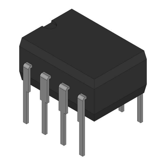
8-Pin DIP or SO-8 Package
APPLICATIONS
3 V to 5 V, 5 V to 12 V Step-Up Converters
9 V to 5 V, 12 V to 5 V Step-Down Converters
Laptop and Palmtop Computers
Cellular Telephones
Flash Memory VPP Generators
Remote Controls
Peripherals and Add-On Cards
Battery Backup Supplies
Uninterruptible Supplies
Portable Instruments
FUNCTIONAL BLOCK DIAGRAMS
SET
ADP1111
A2
VIN
A0
GAIN BLOCK/
ERROR AMP
ILIM
SW1
1.25V
REFERENCE
OSCILLATOR
A1
COMPARATOR
GND
DRIVER
SW2
FB
SET
ADP1111-5
ADP1111-12
A2
VIN
A0
GAIN BLOCK/
ERROR AMP
ILIM
SW1
1.25V
REFERENCE
R1
A1
OSCILLATOR
COMPARATOR
R2 220k
DRIVER
SW2
GENERAL DESCRIPTION
The ADP1111 is part of a family of step-up/step-down switching regulators that operates from an input voltage supply of 2 V
to 12 V in step-up mode and up to 30 V in step-down mode.
The ADP1111 can be programmed to operate in step-up/stepdown or inverting applications with only 3 external components.
The fixed outputs are 3.3 V, 5 V and 12 V; and an adjustable
version is also available. The ADP1111 can deliver 100 mA at
5 V from a 3 V input in step-up mode, or it can deliver 200 mA
at 5 V from a 12 V input in step-down mode.
GND
SENSE
Maximum switch current can be programmed with a single
resistor, and an open collector gain block can be arranged in
multiple configuration for low battery detection, as a post linear
regulator, undervoltage lockout, or as an error amplifier.
If input voltages are lower than 2 V, see the ADP1110.
REV. 0
Information furnished by Analog Devices is believed to be accurate and
reliable. However, no responsibility is assumed by Analog Devices for its
use, nor for any infringements of patents or other rights of third parties
which may result from its use. No license is granted by implication or
otherwise under any patent or patent rights of Analog Devices.
One Technology Way, P.O. Box 9106, Norwood, MA 02062-9106, U.S.A.
Tel: 617/329-4700
World Wide Web Site: http://www.analog.com
Fax: 617/326-8703
© Analog Devices, Inc., 1996
�ADP1111–SPECIFICATIONS (08C ≤ T ≤ +708C, V
A
IN
= 3 V unless otherwise noted)
Parameter
Conditions
VS
QUIESCENT CURRENT
Switch Off
IQ
INPUT VOLTAGE
Step-Up Mode
Step-Down Mode
VIN
COMPARATOR TRIP POINT
VOLTAGE
ADP11111
VOUT
Min
Typ
Max
Units
300
500
µA
12.6
30.0
V
V
2.0
1.20
1.25
1.30
V
3.13
4.75
11.40
3.30
5.00
12.00
3.47
5.25
12.60
V
V
V
OUTPUT SENSE VOLTAGE
ADP1111-3.3
ADP1111-52
ADP1111-122
COMPARATOR HYSTERESIS
ADP1111
8
12.5
mV
OUTPUT HYSTERESIS
ADP1111-3.3
ADP1111-5
ADP1111-12
21
32
75
50
50
120
mV
mV
mV
OSCILLATOR FREQUENCY
fOSC
54
72
88
kHz
DUTY CYCLE
Full Load
DC
43
50
65
%
SWITCH ON TIME
ILIM Tied to VIN
tON
5
7
9
µs
SW SATURATION VOLTAGE
STEP-UP MODE
TA = +25°C
VIN = 3.0 V, ISW = 650 mA
VIN = 5.0 V, ISW = 1 A
VIN = 12 V, ISW = 650 mA
VSAT
0.5
0.8
1.1
0.65
1.0
1.5
V
V
V
STEP-DOWN MODE
FEEDBACK PIN BIAS CURRENT
ADP1111 VFB = 0 V
IFB
160
300
nA
SET PIN BIAS CURRENT
VSET = VREF
ISET
270
400
nA
GAIN BLOCK OUTPUT LOW
ISINK = 300 µA
VSET = 1.00 V
VOL
0.15
0.4
V
0.02
0.4
0.075
%/V
%/V
REFERENCE LINE REGULATION
5 V ≤ VIN ≤ 30 V
2 V ≤ VIN ≤ 5 V
GAIN BLOCK GAIN
RL = 100 kΩ3
AV
CURRENT LIMIT
TA = +25°C
220 Ω from ILIM to VIN
ILIM
CURRENT LIMIT TEMPERATURE
COEFFICIENT
SWITCH OFF LEAKAGE CURRENT
MAXIMUM EXCURSION BELOW GND
1000
6000
V/V
400
mA
–0.3
%/°C
TA = +25°C
Measured at SW1 Pin
VSW1 = 12 V
1
10
µA
TA = +25°C
ISW1 ≤ 10 µA, Switch Off
–400
–350
mV
NOTES
1
This specification guarantees that both the high and low trip points of the comparator fall within the 1.20 V to 1.30 V range.
2
The output voltage waveform will exhibit a sawtooth shape due to the comparator hysteresis. The output voltage on the fixed output versions will always be within
the specified range.
3
100 kΩ resistor connected between a 5 V source and the AO pin.
4
All limits at temperature extremes are guaranteed via correlation using standard statistical methods.
Specifications subject to change without notice.
–2–
REV. 0
�ADP1111
PIN DESCRIPTIONS
ABSOLUTE MAXIMUM RATINGS
Supply Voltage . . . . . . . . . . . . . . . . . . . . . . . . . . . . . . . . . 36 V
SW1 Pin Voltage . . . . . . . . . . . . . . . . . . . . . . . . . . . . . . . 50 V
SW2 Pin Voltage . . . . . . . . . . . . . . . . . . . . . . . . –0.5 V to VIN
Feedback Pin Voltage (ADP1111) . . . . . . . . . . . . . . . . . 5.5 V
Switch Current . . . . . . . . . . . . . . . . . . . . . . . . . . . . . . . 1.5 A
Maximum Power Dissipation . . . . . . . . . . . . . . . . . . 500 mW
Operating Temperature Range
ADP1111A . . . . . . . . . . . . . . . . . . . . . . . . . . . 0°C to +70°C
Storage Temperature Range . . . . . . . . . . . . . –65°C to 150°C
Lead Temperature (Soldering, 10 sec) . . . . . . . . . . . . . 300°C
TYPICAL APPLICATION
Mnemonic
Function
ILIM
For normal conditions this pin is connected to
VIN. When lower current is required, a resistor
should be connected between ILIM and VIN.
Limiting the switch current to 400 mA is achieved
by connecting a 220 Ω resistor.
Input Voltage.
Collector Node of Power Transistor. For stepdown configuration, connect to VIN. For step-up
configuration, connect to an inductor/diode.
Emitter Node of Power Transistor. For stepdown configuration, connect to inductor/diode.
For step-up configuration, connect to ground.
Do not allow this pin to go more than a diode
drop below ground.
Ground.
Auxiliary Gain (GB) Output. The open collector
can sink 300 µA. It can be left open if unused.
Gain Amplifier Input. The amplifier’s positive
input is connected to SET pin and its negative
input is connected to the 1.25 V reference. It can
be left open if unused.
On the ADP1111 (adjustable) version this pin
is connected to the comparator input. On the
ADP1111-3.3, ADP1111-5 and ADP1111-12,
the pin goes directly to the internal application
resistor that sets output voltage.
VIN
SW1
SW2
SUMIDA
CD54-220K
22µH
MBRS120T3
5V
100mA
3V
INPUT
ILIM
GND
AO
VIN
SW1
10µF
(OPTIONAL)
ADP1111AR-5
33µF
SET
SENSE
GND
SW2
FB/SENSE
Figure 1. 3 V to 5 V Step-Up Converter
ORDERING GUIDE
Model
Output Voltage
Package*
ADP1111AN
ADP1111AR
ADP1111AN-3.3
ADP1111AR-3.3
ADP1111AN-5
ADP1111AR-5
ADP1111AN-12
ADP1111AR-12
ADJ
ADJ
3.3 V
3.3 V
5V
5V
12 V
12 V
N-8
SO-8
N-8
SO-8
N-8
SO-8
N-8
SO-8
PIN CONFIGURATIONS
8-Lead Plastic DIP
(N-8)
8 FB (SENSE)*
ILIM 1
VIN
2
ADP1111
7 SET
SW1
TOP VIEW
3 (Not to Scale) 6 A0
SW2
4
5 GND
8-Lead SOIC
(SO-8)
8 FB (SENSE)*
ILIM 1
ADP1111
SW1
7 SET
TOP VIEW
3 (Not to Scale) 6 A0
SW2
4
VIN
2
5 GND
*N = Plastic DIP, SO = Small Outline Package.
*FIXED VERSIONS
CAUTION
ESD (electrostatic discharge) sensitive device. Electrostatic charges as high as 4000 V readily
accumulate on the human body and test equipment and can discharge without detection.
Although the ADP1111 features proprietary ESD protection circuitry, permanent damage may
occur on devices subjected to high energy electrostatic discharges. Therefore, proper ESD
precautions are recommended to avoid performance degradation or loss of functionality.
REV. 0
–3–
*FIXED VERSIONS
WARNING!
ESD SENSITIVE DEVICE
�ADP1111–Typical Characteristics
76
1.4
75
OSCILLATOR FREQUENCY – kHz
SATURATION VOLTAGE – V
1.2
1.0
0.8
VIN = 3V
VIN = 5V
0.6
VIN = 2V
0.4
0.2
73
OSCILLATOR FREQUENCY
72
71
70
69
68
67
0
0.1
0.2
0.4
0.6
0.8
ISWITCH CURRENT – A
1.0
2
1.2
Figure 2. Saturation Voltage vs. ISWITCH Current in
Step-Up Mode
4
6
8
10
12 15
18
INPUT VOLTAGE – V
2.0
1.9
1.8
1.7
SWITCH CURRENT – A
1.5
1.4
1.2
21
24
27
30
Figure 5. Oscillator Frequency vs. Input Voltage
1.6
ON VOLTAGE – V
74
VIN = 12V
1.0
0.8
0.6
STEP-DOWN WITH
VIN = 12V
1.3
1.1
0.9
STEP-UP WITH
2V < VIN < 5V
0.7
0.4
0.5
0.2
0.3
0.1
0
0.1
0.2
0.4
0.6
ISWITCH CURRENT – A
0.8
1
0.9
10
RLIM – Ω
100
1000
Figure 6. Maximum Switch Current vs. RLIM
Figure 3. Switch ON Voltage vs. ISWITCH Current In
Step-Down Mode
80
1400
78
OSCILLATOR FREQUENCY – kHz
QUIESCENT CURRENT – µA
1200
1000
QUIESCENT CURRENT
800
600
400
200
0
1.5
76
74
72
OSCILLATOR FREQUENCY
70
68
66
64
62
3
6
9
12
15
18
21
24
27
60
–40
30
0
25
TEMPERATURE – 8C
70
85
INPUT VOLTAGE – V
Figure 4. Quiescent Current vs. Input Voltage
Figure 7. Oscillator Frequency vs. Temperature
–4–
REV. 0
�ADP1111
7.5
1.10
7.4
1.05
7.2
ON VOLTAGE – V
ON TIME – µs
7.3
ON TIME
7.1
7.0
6.9
VIN = 12V @ ISW = 0.65A
1.00
0.95
0.90
6.8
0.85
6.7
6.6
–40
0
25
TEMPERATURE – 8C
70
0.80
–40
85
Figure 8. Switch ON Time vs. Temperature
0
25
TEMPERATURE – 8C
70
85
Figure 11. Switch ON Voltage vs. Temperature in StepDown Mode
58
500
450
QUIESCENT CURRENT – µA
56
DUTY CYCLE – %
DUTY CYCLE
54
52
50
400
350
QUIESCENT CURRENT
300
250
200
150
100
48
50
46
–40
0
25
TEMPERATURE – 8C
70
0
–40
85
Figure 9. Duty Cycle vs. Temperature
70
85
250
0.5
200
VIN = 3V @ ISW = 0.65A
BIAS CURRENT – µA
SATURATION VOLTAGE – V
25
TEMPERATURE – 8C
Figure 12. Quiescent Current vs. Temperature
0.6
0.4
0.3
0.2
0
–40
BIAS CURRENT
150
100
50
0.1
0
25
TEMPERATURE – 8C
70
0
–40
85
Figure 10. Saturation Voltage vs. Temperature in Step-Up
Mode
REV. 0
0
0
25
TEMPERATURE – 8C
70
85
Figure 13. Feedback Bias Current vs. Temperature
–5–
�ADP1111
350
The ADP1111 provides external connections for both the
collector and emitter of its internal power switch that permit
both step-up and step-down modes of operation. For the stepup mode, the emitter (Pin SW2) is connected to GND, and the
collector (Pin SW1) drives the inductor. For step-down mode,
the emitter drives the inductor while the collector is connected
to VIN.
BIAS CURRENT – µA
300
BIAS CURRENT
250
200
150
The output voltage of the ADP1111 is set with two external
resistors. Three fixed-voltage models are also available:
ADP1111–3.3 (+3.3 V), ADP1111–5 (+5 V) and ADP1111–12
(+12 V). The fixed-voltage models are identical to the
ADP1111, except that laser-trimmed voltage-setting resistors
are included on the chip. On the fixed-voltage models of the
ADP1111, simply connect the feedback pin (Pin 8) directly to
the output voltage.
100
50
0
–40
0
25
TEMPERATURE – 8C
70
85
Figure 14. Set Pin Bias Current vs. Temperature
COMPONENT SELECTION
General Notes on Inductor Selection
THEORY OF OPERATION
When the ADP1111 internal power switch turns on, current
begins to flow in the inductor. Energy is stored in the inductor
core while the switch is on, and this stored energy is transferred
to the load when the switch turns off. Since both the collector
and the emitter of the switch transistor are accessible on the
ADP1111, the output voltage can be higher, lower, or of
opposite polarity than the input voltage.
The ADP1111 is a flexible, low-power, switch-mode power
supply (SMPS) controller. The regulated output voltage can be
greater than the input voltage (boost or step-up mode) or less
than the input (buck or step-down mode). This device uses a
gated-oscillator technique to provide very high performance
with low quiescent current.
A functional block diagram of the ADP1111 is shown on
the first page of this data sheet. The internal 1.25 V reference is
connected to one input of the comparator, while the other input
is externally connected (via the FB pin) to a feedback network
connected to the regulated output. When the voltage at the FB
pin falls below 1.25 V, the 72 kHz oscillator turns on. A driver
amplifier provides base drive to the internal power switch, and
the switching action raises the output voltage. When the voltage
at the FB pin exceeds 1.25 V, the oscillator is shut off. While
the oscillator is off, the ADP1111 quiescent current is only
300 µA. The comparator includes a small amount of hysteresis,
which ensures loop stability without requiring external components for frequency compensation.
To specify an inductor for the ADP1111, the proper values of
inductance, saturation current and dc resistance must be
determined. This process is not difficult, and specific equations
for each circuit configuration are provided in this data sheet. In
general terms, however, the inductance value must be low
enough to store the required amount of energy (when both
input voltage and switch ON time are at a minimum) but high
enough that the inductor will not saturate when both VIN and
switch ON time are at their maximum values. The inductor
must also store enough energy to supply the load, without
saturating. Finally, the dc resistance of the inductor should be
low so that excessive power will not be wasted by heating the
windings. For most ADP1111 applications, an inductor of
15 µH to 100 µH with a saturation current rating of 300 mA to
1 A and dc resistance 6.2 V
INCREASING OUTPUT CURRENT IN THE STEP-DOWN
REGULATOR
L1
VOUT
D1
1N5818
+
R2
CL
R1
NC
Figure 19. Step-Down Mode Operation
When the switch turns off, the magnetic field collapses. The
polarity across the inductor changes, and the switch side of the
inductor is driven below ground. Schottky diode D1 then turns
on, and current flows into the load. Notice that the Absolute
Maximum Rating for the ADP1111’s SW2 pin is 0.5 V below
ground. To avoid exceeding this limit, D1 must be a Schottky
diode. If a silicon diode is used for D1, Pin SW2 can go to
–0.8 V, which will cause potentially damaging power dissipation
within the ADP1111.
The output voltage of the buck regulator is fed back to the
ADP1111’s FB pin by resistors R1 and R2. When the voltage at
pin FB falls below 1.25 V, the internal power switch turns “on”
again, and the cycle repeats. The output voltage is set by the
formula:
VOUT
VOUT
FB 8
SW1
ADP1111
NC
3
If the input voltage to the ADP1111 varies over a wide range, a
current limiting resistor at Pin 1 may be required. If a particular
circuit requires high peak inductor current with minimum input
supply voltage, the peak current may exceed the switch maximum rating and/or saturate the inductor when the supply
voltage is at the maximum value. See the “Limiting the Switch
Current” section of this data sheet for specific recommendations.
VIN
+
2
ADP1111
where 7 µs is the ADP1111 switch’s “on” time.
C2
R3
ILIM VIN SW1
A typical configuration for step down operation of the ADP1111
is shown in Figure 19. In this case, the collector of the internal
power switch is connected to VIN and the emitter drives the
inductor. When the switch turns on, SW2 is pulled up towards
VIN. This forces a voltage across L1 equal to VIN – VCE – VOUT
and causes current to flow in L1. This current reaches a final
value of:
I PEAK ≅
+
Unlike the boost configuration, the ADP1111’s internal power
switch is not saturated when operating in step-down mode. A
conservative value for the voltage across the switch in step-down
mode is 1.5 V. This results in high power dissipation within the
ADP1111 when high peak current is required. To increase the
output current, an external PNP switch can be added (Figure
21). In this circuit, the ADP1111 provides base drive to Q1
through R3, while R4 ensures that Q1 turns off rapidly. Because
the ADP1111’s internal current limiting function will not work
in this circuit, R5 is provided for this purpose. With the value
shown, R5 limits current to 2 A. In addition to reducing power
dissipation on the ADP1111, this circuit also reduces the switch
voltage. When selecting an inductor value for the circuit of
Figure 21, the switch voltage can be calculated from the
formula:
V SW = V R5 + V Q1(SAT) ≅ 0.6 V + 0.4 V ≅ 1 V
R2
= 1.25 V • 1 +
R1
INPUT
+
CINPUT
R5
0.3Ω
R4
220Ω
1
ILIM
2 VIN
SW1 3
R3
330Ω
Q1
MJE210
L1
OUTPUT
ADP1111
R2
FB 8
AO SET GND SW2
When operating the ADP1111 in step-down mode, the output
voltage is impressed across the internal power switch’s emitterbase junction when the switch is off. To protect the switch, the
output voltage should be limited to 6.2 V or less. If a higher
output voltage is required, a Schottky diode should be placed in
series with SW2 as shown in Figure 20.
6
7
NC
NC
5
4
D1
1N5821
+
R1
CL
Figure 21. High Current Step-Down Operation
–10–
REV. 0
�ADP1111
Table I. Component Selection for Typical Converters
Input
Voltage
Output
Voltage
Output
Current (mA)
Circuit
Figure
Inductor
Value
Inductor
Part No.
Capacitor
Value
2 to 3.1
2 to 3.1
2 to 3.1
2 to 3.1
5
5
6.5 to 11
12 to 20
20 to 30
5
12
5
5
12
12
12
12
5
5
5
–5
–5
90 mA
10 mA
30 mA
10 mA
90 MA
30 mA
50 mA
300 mA
300 mA
7 mA
250 mA
4
4
4
4
4
4
5
5
5
6
6
15 µH
47 µH
15 µH
47 µH
33 µH
47 µH
15 µH
56 µH
120 µH
56 µH
120 µH
CD75-150K
CTX50-1
CD75-150K
CTX50-1
CD75-330K
CTX50-1
33 µF
10 µF
22 µF
10 µF
22 µF
15 µF
47 µF
47 µF
47 µF
47 µF
100 µF
CTX50-4
CTX100-4
CTX50-4
CTX100-4
Notes
*
**
**
**
**
NOTES
CD = Sumida.
CTX = Coiltronics.
**Add 47 Ω from ILIM to VIN.
**Add 220 Ω from ILIM to VIN.
POSITIVE-TO-NEGATIVE CONVERSION
The ADP1111 can convert a positive input voltage to a negative
output voltage as shown in Figure 22. This circuit is essentially
identical to the step-down application of Figure 19, except that
the “output” side of the inductor is connected to power ground.
When the ADP1111’s internal power switch turns off, current
flowing in the inductor forces the output (–VOUT) to a negative
potential. The ADP1111 will continue to turn the switch on
until its FB pin is 1.25 V above its GND pin, so the output
voltage is determined by the formula:
also reduces the circuit’s output voltage sensitivity to temperature, which otherwise would be dominated by the –2 mV VBE
contribution of Q1. The output voltage for this circuit is
determined by the formula:
VOUT = 1.25 V •
R2
R1
Unlike the positive step-up converter, the negative-to-positive
converter’s output voltage can be either higher or lower than the
input voltage.
R2
VOUT = 1.25 V • 1 +
R1
L1
D1
1N5818
+
R2
RLIM
Q1
INPUT
+
CINPUT
+
RLIM
C2
1
2
ILIM VIN
L1
NC
NC
5
R2
D1
1N5818
+
R1
NEGATIVE
INPUT
CL
NEGATIVE
OUTPUT
Figure 22. Positive-to-Negative Converter
The design criteria for the step-down application also apply to
the positive-to-negative converter. The output voltage should be
limited to |6.2 V| unless a diode is inserted in series with the
SW2 pin (see Figure 20.) Also, D1 must again be a Schottky
diode to prevent excessive power dissipation in the ADP1111.
NEGATIVE-TO-POSITIVE CONVERSION
The circuit of Figure 23 converts a negative input voltage to a
positive output voltage. Operation of this circuit configuration is
similar to the step-up topology of Figure 18, except the current
through feedback resistor R2 is level-shifted below ground by a
PNP transistor. The voltage across R2 is VOUT –VBEQ1. However, diode D2 level-shifts the base of Q1 about 0.6 V below
ground thereby cancelling the VBE of Q1. The addition of D2
REV. 0
ILIM
VIN
D2
2N3906
CL
MJE210
SW1 3
FB 8
AO SET GND SW2
OUTPUT
FB 8
AO SET GND
7
2
ADP1111
3
SW1
SW2 4
ADP1111
6
1
POSITIVE
OUTPUT
6
7
NC
NC
5
4
10kΩ
R1
Figure 23. ADP1111 Negative-to-Positive Converter
LIMITING THE SWITCH CURRENT
The ADP1111’s RLIM pin permits the switch current to be
limited with a single resistor. This current limiting action occurs
on a pulse by pulse basis. This feature allows the input voltage
to vary over a wide range without saturating the inductor or
exceeding the maximum switch rating. For example, a particular
design may require peak switch current of 800 mA with a 2.0 V
input. If VIN rises to 4 V, however, the switch current will
exceed 1.6 A. The ADP1111 limits switch current to 1.5 A and
thereby protects the switch, but the output ripple will increase.
Selecting the proper resistor will limit the switch current to
800 mA, even if VIN increases. The relationship between RLIM
and maximum switch current is shown in Figure 6.
The ILIM feature is also valuable for controlling inductor current
when the ADP1111 goes into continuous-conduction mode.
–11–
�ADP1111
RLIM
(EXTERNAL)
This occurs in the step-up mode when the following condition is
met:
VIN
ILIM
VIN
VOUT + VDIODE
1
<
VIN − VSW
1 − DC
R1
80Ω
(INTERNAL)
Q3
where DC is the ADP1111’s duty cycle. When this relationship
exists, the inductor current does not go all the way to zero
during the time that the switch is OFF. When the switch turns
on for the next cycle, the inductor current begins to ramp up
from the residual level. If the switch ON time remains constant,
the inductor current will increase to a high level (see Figure 24).
This increases output ripple and can require a larger inductor
and capacitor. By controlling switch current with the ILIM
resistor, output ripple current can be maintained at the design
values. Figure 25 illustrates the action of the ILIM circuit.
IQ1
ADP1111
DRIVER
72kHz
OSC
200
SW1
Q2
Q1
POWER
SWITCH
SW2
Figure 26. ADP1111 Current Limit Operation
The delay through the current limiting circuit is approximately
1 µs. If the switch ON time is reduced to less than 3 µs, accuracy
of the current trip-point is reduced. Attempting to program a
switch ON time of 1 µs or less will produce spurious responses
in the switch ON time; however, the ADP1111 will still provide
a properly regulated output voltage.
PROGRAMMING THE GAIN BLOCK
The gain block of the ADP1111 can be used as a low-battery
detector, error amplifier or linear post regulator. The gain block
consists of an op amp with PNP inputs and an open-collector
NPN output. The inverting input is internally connected to the
ADP1111’s 1.25 V reference, while the noninverting input is
available at the SET pin. The NPN output transistor will sink
about 300 µA.
200mA/div
Figure 24.
Figure 27a shows the gain block configured as a low-battery
monitor. Resistors R1 and R2 should be set to high values to
reduce quiescent current, but not so high that bias current in
the SET input causes large errors. A value of 33 kΩ for R2 is a
good compromise. The value for R1 is then calculated from the
formula:
R1 =
V LOBATT − 1.25 V
1.25 V
R2
where VLOBATT is the desired low battery trip point. Since the
gain block output is an open-collector NPN, a pull-up resistor
should be connected to the positive logic power supply.
200mA/div
5V
Figure 25.
RL
47k
VIN
ADP1111
The internal structure of the ILIM circuit is shown in Figure 26.
Q1 is the ADP1111’s internal power switch that is paralleled by
sense transistor Q2. The relative sizes of Q1 and Q2 are scaled
so that IQ2 is 0.5% of IQ1. Current flows to Q2 through an
internal 80 Ω resistor and through the RLIM resistor. These two
resistors parallel the base-emitter junction of the oscillatordisable transistor, Q3. When the voltage across R1 and RLIM
exceeds 0.6 V, Q3 turns on and terminates the output pulse. If
only the 80 Ω internal resistor is used (i.e. the ILIM pin is
connected directly to VIN), the maximum switch current will be
1.5 A. Figure 6 gives RLIM values for lower current-limit values.
R1
VBAT
1.25V
REF
AO
SET
33k
R2
TO
PROCESSOR
GND
VLB–1.25V
R1= –––––––––
35.1µA
VLB = BATTERY TRIP POINT
Figure 27a. Setting the Low Battery Detector Trip Point
–12–
REV. 0
�ADP1111
The circuit of Figure 27b may produce multiple pulses when
approaching the trip point due to noise coupled into the SET
input. To prevent multiple interrupts to the digital logic,
hysteresis can be added to the circuit (Figure 27). Resistor
RHYS, with a value of 1 MΩ to 10 MΩ, provides the hysteresis.
The addition of RHYS will change the trip point slightly, so the
new value for R1 will be:
9 V to 5 V Step-Down Converter
This circuit uses a 9 V battery to generate a +5 V output. The
circuit will work down to 6.5 V, supplying 50 mA at this lower
limit. Switch current is limited to around 500 mA by the 100 Ω
resistor.
INPUT
9V
V LOBATT − 1.25 V
R1 =
1.25 V V L − 1.25 V
R2 − R + R
L
HYS
RLIM
100Ω
NC
RL
47k
1.25V
REF
AO
TO
PROCESSOR
GND
R2
D1
1N5818
+
CL
22µF
NC
20 V to 5 V Step-Down Converter
SET
33k
OUTPUT
(9VIN TO 5V @ 150mA,
6.5VIN TO 5V @ 50mA)
15µH
Figure 29. 9 V to 5 V Step-Down Converter
ADP1111
R1
L1
CTX15-4
SENSE 8
AO SET GND
6
7
5
5V
VBAT
3
SW1
SW2 4
ADP1111-5
where VL is the logic power supply voltage, RL is the pull-up
resistor, and RHYS creates the hysteresis.
VIN
2
1
ILIM VIN
1.6M
This circuit is similar to Figure 29, except it supplies much
higher output current and operates over a much wider range of
input voltage. As in the previous examples, switch current is
limited to 500 mA.
RHYS
12V TO 28V
INPUT
RLIM
100Ω
Figure 27b.
APPLICATION CIRCUITS
All Surface Mount 3 V to 5 V Step-Up Converter
INPUT +3V
R3*
(OPTIONAL)
L1
20µH
CTX20-4
MBRS120T3
SENSE 8
AO SET GND
6
7
5
SW1 3
ADP1111-5
SENSE 8
AO SET GND SW2
6
7
5
NC
OUTPUT
(+5V @ 300mA)
68µH
D1
1N5818
+
CL
47µF
NC
Figure 30. 20 V to 5 V Step-Down Converter
OUTPUT
(5V @ 100mA)
+
This circuit is essentially identical to Figure 22, except it uses a
fixed-output version of the ADP1111 to simplify the design
somewhat.
12V TO 28V
INPUT
CL
33µF
RLIM
100Ω
1
4
2
ILIM VIN
NC
L1
CTX68-4
+5 V to –5 V Converter
2
1
ILIM VIN
3
SW1
SW2 4
ADP1111-5
This is the most basic application (along with the basic stepdown configuration to follow) of the ADP1111. It takes full
advantage of surface mount packaging for all the devices used in
the design. The circuit can provide +5 V at 100 mA of output
current and can be operated off of battery power for use in
portable equipment.
D1
2
1
ILIM VIN
3
SW1
SW2 4
ADP1111-5
NC
SENSE 8
AO SET GND
6
7
5
Figure 28. All Surface Mount +3 V to +5 V Step-Up Converter
NC
L1
CTX33-2
33µH
D1
1N5818
+
CL
33µF
NC
Figure 31. +5 V to –5 V Converter
REV. 0
–13–
–5V
@ 75mA
�ADP1111
Voltage-Controlled Positive-to-Negative Converter
High Power, Low Quiescent Current Step-Down Converter
By including an op amp in the feedback path, a simple positiveto-negative converter can be made to give an output that is a
linear multiple of a controlling voltage, Vc. The op amp, an
OP196, rail-to-rail input and output amplifier, sums the
currents from the output and controlling voltage and drives the
FB pin either high or low, thereby controlling the on-board
oscillator. The 0.22 Ω resistor limits the short-circuit current to
about 3 A and, along with the BAT54 Schottky diode, helps
limit the peak switch current over varying input voltages. The
external power switch features an active pull-up to speed up the
turn-off time of the switch. Although an IRF9530 was used in
the evaluation, almost any device that can handle at least 3 A of
peak current at a VDS of at least 50 V is suitable for use in this
application, provided that adequate attention is paid to power
dissipation. The circuit can deliver 2 W of output power with a
+6-volt input from a control voltage range of 0 V to 5 V.
By making use of the fact that the feedback pin directly controls
the internal oscillator, this circuit achieves a shutdown-like state
by forcing the feedback pin above the 1.25 V comparator
threshold. The logic level at the 1N4148 diode anode needs to
be at least 2 V for reliable standby operation.
The external switch driver circuit features an active pull-up
device, a 2N3904 transistor, to ensure that the power MOSFET
turns off quickly. Almost any power MOSFET will do as the
switch as long as the device can withstand the 18 volt VGS and is
reasonably robust. The 0.22 Ω resistor limits the short-circuit
current to about 3 A and, along with the BAT54 Schottky
diode, helps to limit the peak switch current over varying input
voltages.
+8V TO +18V
IRF9540
S
D
RLIM
INPUT
0.22
+5V TO +12V
BAT54
RLIM
INPUT
0.22Ω
BAT54
2kΩ
2
1
VIN
ILIM
7
5
SW1 3
1N4148
1kΩ
6
7
2
200kΩ
NC
39kΩ
+3 V to –22 V LCD Bias Generator
This circuit uses an adjustable-output version of the ADP1111
to generate a +22.5 V reference output that is level-shifted to
give an output of –22 V. If operation from a +5 volt supply is
desired, change R1 to 47 ohms. The circuit will deliver 7 mA
with a 3 volt supply and 40 mA with a 5 volt supply.
2xAA
CELLS
1
2
VIN
6
7
NC
NC
5
4
1N4148
LI = COILTRONICS CTX20-4
Figure 34. High Power, Low Quiescent Current Step-Down
Converter
NOTES
1. All inductors referenced are Coiltronics CTX-series except
where noted.
2. If the source of power is more than an inch or so from the
converter, the input to the converter should be bypassed with
approximately 10 µF of capacitance. This capacitor should
be a good quality tantalum or aluminum electrolytic.
OUTPUT
25µH
ILIM
121kΩ
D1
1N4148
L1
+3V
1N4148
VC (0V TO +5V)
Figure 32. Voltage Controlled Positive-to-Negative
Converter
RLIM
100Ω
SW1 3
OPERATE/STANDBY
2V ≤ VIN ≤ 5
–VOUT = –5.13 *VC
2W MAXIMUM OUTPUT
1N5231 4
NC
CL
220µF
40.2kΩ
OUTPUT
3
51Ω
+
D1
IN5821
+5V
500mA
FB 8
AO SET GND SW2
CTX20-4
CL +
47µF
35V
D1
IN5821
VIN
4
1
ILIM
2N3904
ADP1111
L1 20µH
FB 8
AO SET GND SW2
6
2
VIN
51Ω
2N3904
ADP1111
G
2k
IRF9530
LI
20µH
SW1 3
732kΩ
CL
0.1µF
ADP1111
FB 8
+
AO SET GND SW2 4.7
µF
6
7
5
4
42.2kΩ
1N5818
NC
NC
L1 = CTX25-4
+
1N5818
22µF
–22V OUTPUT
7mA @ 2V INPUT
Figure 33. 3 V to –22 V LCD Bias Generator
–14–
REV. 0
�ADP1111
OUTLINE DIMENSIONS
Dimensions shown in inches and (mm).
8-Lead Plastic DIP
(N-8)
0.430 (10.92)
0.348 (8.84)
8
5
0.280 (7.11)
0.240 (6.10)
1
4
0.060 (1.52)
0.015 (0.38)
PIN 1
0.210 (5.33)
MAX
0.325 (8.25)
0.300 (7.62)
0.195 (4.95)
0.115 (2.93)
0.130
(3.30)
MIN
0.160 (4.06)
0.115 (2.93)
0.022 (0.558) 0.100 0.070 (1.77)
0.014 (0.356) (2.54) 0.045 (1.15)
BSC
0.015 (0.381)
0.008 (0.204)
SEATING
PLANE
8-Lead SOIC
(SO-8)
0.1968 (5.00)
0.1890 (4.80)
0.1574 (4.00)
0.1497 (3.80)
PIN 1
0.0098 (0.25)
0.0040 (0.10)
SEATING
PLANE
REV. 0
8
5
1
4
0.2440 (6.20)
0.2284 (5.80)
0.0688 (1.75)
0.0532 (1.35)
0.0500 0.0192 (0.49)
(1.27) 0.0138 (0.35)
BSC
0.0196 (0.50)
x 45°
0.0099 (0.25)
0.0098 (0.25)
0.0075 (0.19)
–15–
8°
0°
0.0500 (1.27)
0.0160 (0.41)
�–16–
PRINTED IN U.S.A.
C2213–12–10/96
�