650 kHz/1.3 MHz Step-Up Converter
Evaluation Board Documentation
EVAL-ADP1612/ADP1613
The ADP1612/ADP1613 evaluation module operates in
pulse-width modulation (PWM) current mode with up to 94%
efficiency. The shunt-selectable switching frequency and PWM
current-mode architecture allow for excellent transient response,
easy noise filtering, and the use of small, cost-saving external
inductors and capacitors. Other key features include a 33 nF
soft start capacitor, undervoltage lockout (UVLO), thermal
shutdown (TSD), and jumper selected enable. The evaluation
module demonstrates the operation and performance of the
ADP1612/ADP1613.
FEATURES
Input voltage range
1.8 V to 5.5 V for the ADP1612-5-EVALZ
2.5 V to 5.5 V for the ADP1613-12-EVALZ
Output voltage
5 V for ADP1612-5-EVALZ
12 V for ADP1613-12-EVALZ
Shunt-selectable 1.3 MHz or 650 kHz switching frequency
Jumper for enable/shutdown control
Components optimized for the indicated output voltages
This data sheet includes I/O descriptions, setup instructions,
the schematic, and the PCB layout drawings for the ADP1612/
ADP1613 step-up converter evaluation module. Use this data
sheet in conjunction with the ADP1612/ADP1613 data sheet
available on www.analog.com.
GENERAL DESCRIPTION
The ADP1612/ADP1613 evaluation module is a complete stepup dc-to-dc switching converter application with components
selected to allow operation over the full range of input and load
conditions for the 5 V (ADP1612) and 12 V (ADP1613) output
voltages. The evaluation boards can be adjusted for different
output voltages by changing R1 and R2. In addition, L1, D1, C3,
and R3 may need to be adjusted and should be recalculated to
ensure stable operation.
TYPICAL APPLICATION CIRCUIT
L1
ADP1612/
ADP1613
VIN
6
VIN
3
EN
U1
D1
ON
CIN
R1
FB 2
1.3MHz
650kHz
(DEFAULT)
7
FREQ
8
SS
CSS
R2
COMP 1
GND
4
RCOMP
CCOMP
COUT
06772-002
OFF
VOUT
SW 5
Figure 1. Step-Up Regulator Configuration
Rev. A
Evaluation boards are only intended for device evaluation and not for production purposes.
Evaluation boards are supplied “as is” and without warranties of any kind, express, implied, or
statutory including, but not limited to, any implied warranty of merchantability or fitness for a
particular purpose. No license is granted by implication or otherwise under any patents or other
intellectual property by application or use of evaluation boards. Information furnished by Analog
Devices is believed to be accurate and reliable. However, no responsibility is assumed by Analog
Devices for its use, nor for any infringements of patents or other rights of third parties that may result
from its use. Analog Devices reserves the right to change devices or specifications at any time
without notice. Trademarks and registered trademarks are the property of their respective owners.
Evaluation boards are not authorized to be used in life support devices or systems.
One Technology Way, P.O. Box 9106, Norwood, MA 02062-9106, U.S.A.
www.analog.com
Tel: 781.329.4700
Fax: 781.461.3113 ©2009–2010 Analog Devices, Inc. All rights reserved.
�EVAL-ADP1612/ADP1613
TABLE OF CONTENTS
Features .............................................................................................. 1
Evaluation Board Schematic and Layout .......................................5
General Description ......................................................................... 1
Layout Guidelines..........................................................................5
Typical Application Circuit ............................................................. 1
Ordering Information .......................................................................6
Revision History ............................................................................... 2
Bill of Materials ..............................................................................6
Evaluation Board Hardware ............................................................ 3
Ordering Guide .............................................................................7
Input/Output Connectors ........................................................... 3
ESD Caution...................................................................................7
Evaluation Setup ........................................................................... 3
Performance Evaluation .............................................................. 4
REVISION HISTORY
1/10—Rev. 0 to Rev. A
Changes to Figure 4 to Figure 6 ...................................................... 3
12/09—Revision 0: Initial Version
Rev. A | Page 2 of 8
�EVAL-ADP1612/ADP1613
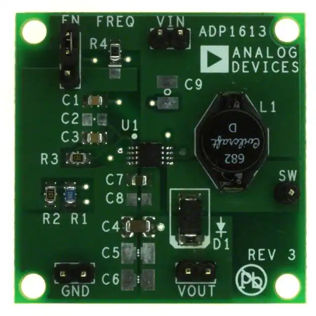
EVALUATION BOARD HARDWARE
The ADP1612/ADP1613 evaluation module is fully assembled
and tested. The following sections describe the various connectors on the board, the proper evaluation setup, and the testing
capabilities of the evaluation module.
VOUT Test Bus
INPUT/OUTPUT CONNECTORS
VIN Test Bus
EN Test Bus
The VIN test bus connects the positive input supply voltage to
the VIN pin. Connect the power supply to this bus and keep the
wires as short as possible to minimize the EMI transmission.
The EN connector is used to enable/disable the converter via
the EN pin. Use one of the following methods to enable the
converter. Do not leave the EN pin floating.
•
GND Test Bus
The GND test bus is the power ground connection for the part
via the GND pin as well as the bypass capacitors. Connect
ground connections from external equipment to this bus.
Use a jumper to connect the top two pins of the EN test
bus. This connects EN to VIN and enables the converter
(see Figure 2).
SW Test Point
08527-003
PLACE
JUMPER
HERE
The SW test point is for measuring the switch node (SW pin)
behavior and switching frequency.
Figure 2. Enabled Jumper Position
•
The output voltage at the VOUT test bus is set by the resistive
voltage divider network, R1 and R2. A load can be attached to
the VOUT test bus.
Use a jumper to connect the bottom two pins of the EN test
bus. This connects EN to GND and disables the converter
(see Figure 3).
EVALUATION SETUP
Follow these setup instructions to ensure proper operation of
the ADP1612/ADP1613 evaluation module:
08527-004
1.
PLACE
JUMPER
HERE
Figure 3. Disabled Jumper Position
•
Alternatively, connect a voltage between VIN and GND to
the center pin of the EN test bus for independent control of
the EN pin voltage (see Figure 4).
08527-005
CONNECT
EXTERNAL
DEVICE
HERE
Figure 4. EN Pin Direct Connection
0 Ω Shunt FREQ (R4)
2.
3.
4.
5.
6.
This shunt selects the switching frequency via the FREQ pin.
Several methods are available as follows.
Shunt the top pads of FREQ (R4) for 1.3 MHz operation
(see Figure 5).
PLACE
SHUNT
HERE
08527-006
•
Figure 5. 1.3 MHz Operation Shunt Position
Shunt the bottom pads of FREQ (R4) for 650 kHz
operation (see Figure 6).
PLACE
SHUNT
HERE
08527-007
•
Figure 6. 650 kHz Operation Shunt Position
•
If this shunt is left open, the part defaults to 650 kHz.
Rev. A | Page 3 of 8
Select the passive components for the bypass capacitance,
desired output voltage, compensation, and start-up time,
using the applications information from the ADP1612/
ADP1613 data sheet.
Connect the input supply ground to GND.
Connect the positive input supply to VIN.
Connect the desired load between VOUT and GND. The
maximum continuous output current of the ADP1612/
ADP1613 is dependent upon the input and output
conditions.
Apply a voltage between 1.8 V and 5.5 V (ADP1612) or
2.5 V and 5.5 V (ADP1613) to the VIN test bus.
Move the jumper on the EN test bus to the enabled position.
�EVAL-ADP1612/ADP1613
PERFORMANCE EVALUATION
Line Transient
The following sections discuss tests and the resulting oscilloscope waveforms. Oscilloscope waveforms and typical
performance characteristics are provided in the ADP1612/
ADP1613 data sheet.
The line transient performance is evaluated by generating a
high speed voltage transient on the input (VIN) and observing
the behavior of the evaluation module at the inductor (SW) and
the output (VOUT.)
Line Regulation
Load Transient
The line regulation is observed and measured by monitoring
the output voltage (VOUT) while varying the input voltage (VIN).
The load transient performance is evaluated by generating a fast
current transient on the output (VOUT) and observing the
behavior of the evaluation module at the inductor (SW) and the
output (VOUT.)
Load Regulation
The load regulation is observed and measured by monitoring
the output voltage (VOUT) while sweeping the applied load
between VOUT and GND. To minimize voltage drop, use short
low resistance wires, especially for heavy loads.
Oscillator Frequency
The oscillator frequency can be measured by connecting an
oscilloscope to the SW pin.
Efficiency
Inductor Current
The efficiency, η, is measured by comparing the input power to
the output power
The inductor current is made accessible by removing one side
of the inductor from its pad and connecting a current loop in
series. Place an oscilloscope current probe on the loop to view
the current waveform.
η=
VOUT × I OUT
V IN × I IN
Rev. A | Page 4 of 8
�EVAL-ADP1612/ADP1613
EVALUATION BOARD SCHEMATIC AND LAYOUT
L1
SW
ADP1612/
ADP1613
VIN
EN
6
VIN
3
EN
7
FREQ
8
SS
U1
VOUT
D1
SW 5
R1
FB 2
C7
C8
C9
R2
COMP 1
GND
C1
C4
R3
4
C3
C2
C5
C6
GND
08527-008
FREQ
R4
Figure 7. ADP1612/ADP1613Boost Application Evaluation Board Schematic
LAYOUT GUIDELINES
For high efficiency, good regulation, and stability, a welldesigned printed circuit board (PCB) layout is essential.
Use the following guidelines when designing PCBs:
•
•
•
08527-009
•
•
Figure 8. ADP1612/ADP1613 Boost Application PCB Top Layer
•
•
08527-010
•
Figure 9. ADP1612/ADP1613 Boost Application PCB Bottom Layer
Rev. A | Page 5 of 8
Keep the low ESR input capacitor, CIN (labeled as C7 in
Figure 8), close to VIN and GND. This minimizes noise
injected into the part from board parasitic inductance.
Keep the high current path from CIN (labeled as C7 in
Figure 8) through the L1 inductor to SW and GND as
short as possible.
Keep the high current path from VIN through L1, the
rectifier (D1), and the output capacitor, COUT (labeled as
C4 in Figure 8), as short as possible.
Keep high current traces as short and as wide as possible.
Place the feedback resistors as close to FB as possible to
prevent noise pickup. Connect the ground of the feedback
network directly to an AGND plane to make a Kelvin
connection to the GND pin.
Place the compensation components as close as possible to
COMP. Connect the ground of the compensation network
directly to an AGND plane that makes a Kelvin connection
to the GND pin.
Connect the soft start capacitor, CSS (labeled as C1 in
Figure 8), as close to the device as possible. Connect the
ground of the soft start capacitor to an AGND plane that
makes a Kelvin connection to the GND pin.
Avoid routing high impedance traces from the compensation and feedback resistors near any node connected to SW
or near the inductor to prevent radiated noise injection.
�EVAL-ADP1612/ADP1613
ORDERING INFORMATION
BILL OF MATERIALS
Table 1. ADP1612 (VOUT = 5 V)
Qty
1
1
1
1
1
1
1
1
1
1
1
10
1
Reference
Designator
U1
L1
D1
C1
C2
C3
C4
C5
C6
C7
C8
C9
R1
R2
R3
FREQ/R4
EN, VIN, SW,
VOUT, GND
Description
ADP1612 step-up converter
Inductor, 4.7 μH
Diode
Soft start capacitor, MLCC, 33 nF, 50 V, 0805, ±10%
Compensation capacitor
Compensation capacitor, 1200 pF, 50 V, 0805, ±10%
Output capacitor, 10 µF, 25 V, 1206, ±10%
Output capacitor
Output capacitor
Input capacitor, 10 μF, 16 V, 0805, ±10%
Input capacitor
Input capacitor
Output voltage divider, 30.0 kΩ, 0805, ±1%
Output voltage divider, 10.0 kΩ, 0805, ±1%
Compensation resistor, 12 kΩ, 0805, ±5%
Frequency select shunt resistor, 0 Ω, 0805, 1.3 MHz (top 2 pads)
Header (0.10”, single/double row, straight)
Manufacturer 1
Analog Devices, Inc.
Coilcraft
ON Semiconductor
Panasonic–ECG
Open
Panasonic–ECG
Taiyo Yuden
Open
Open
Taiyo Yuden
Open
Open
Yageo
Vishay/Dale
Yageo
Yageo
Sullins Electronics
Part Number
ADP1612
DO3316P-472ML
MBRS2040LT3
ECJ-2VB1H333K
ECJ-2VB1H122K
TMK316BJ106KL-T
EMK212BJ106KG-T
RC0805FR-0730KL
CRCW080510K0FKEA
RC0805JR-0712KL
RC0805JR-070RL
PBC36SAAN
Equivalent substitutions may be made for all resistors and capacitors.
Table 2. ADP1613 (VOUT = 12 V)
Qty
1
1
1
1
1
1
1
1
1
1
1
10
1
Reference
Designator
U1
L1
D1
C1
C2
C3
C4
C5
C6
C7
C8
C9
R1
R2
R3
FREQ/R4
EN, VIN, SW,
VOUT, GND
Description
ADP1613 step-up converter
Inductor, 6.8 μH
Diode
Soft start capacitor, 33 nF, 50 V, 0805, ±10%
Compensation capacitor
Compensation capacitor, 1000 pF, 50 V, 0805, ±10%
Output capacitor, 10 μF, 25 V, 1206, ±10%
Output capacitor
Output capacitor
Input capacitor, 10 μF, 16 V, 0805, ±10%
Input capacitor
Input capacitor
Output voltage divider, 86.6 kΩ, 0805, ±1%
Output voltage divider, 10.0 kΩ, 0805, ±1%
Compensation resistor, 10 kΩ, 0805, ±5%
Frequency select shunt resistor, 0 Ω, 0805, 1.3 MHz (top 2 pads)
Header (0.10”, single/double row, straight)
Equivalent substitutions may be made for all resistors and capacitors.
Rev. A | Page 6 of 8
Manufacturer 1
Analog Devices, Inc.
Coilcraft
ON Semiconductor
Panasonic–ECG
Open
Panasonic–ECG
Taiyo Yuden
Open
Open
Taiyo Yuden
Open
Open
Yageo
Vishay/Dale
Yageo
Yageo
Sullins Electronics
Part Number
ADP1613
DO3316P-682ML
MBRA340T3G
ECJ-2VB1H333K
ECJ-2VB1H102K
TMK316BJ106KL-T
EMK212BJ106KG-T
RC0805FR-0786K6L
CRCW080510K0FKEA
RC0805JR-0710KL
RC0805JR-070RL
PBC36SAAN
�EVAL-ADP1612/ADP1613
ORDERING GUIDE
Model1
ADP1612-5-EVALZ
ADP1612-BL1-EVZ
ADP1613-12-EVALZ
ADP1613-BL1-EVZ
1
ESD CAUTION
Description
ADP1612 Evaluation Board, 5 V
Output Voltage Configuration
ADP1612 Blank Evaluation Board
ADP1613 Evaluation Board,
12 V Output Voltage Configuration
ADP1613 Blank Evaluation Board
Z = RoHS Compliant Part.
Rev. A | Page 7 of 8
�EVAL-ADP1612/ADP1613
NOTES
©2009–2010 Analog Devices, Inc. All rights reserved. Trademarks and
registered trademarks are the property of their respective owners.
EB08527-0-1/10(A)
Rev. A | Page 8 of 8
�