Data Sheet
ADP1765
5 A, Low VIN, Low Noise, CMOS Linear Regulator
FEATURES
►
►
►
►
►
►
►
►
►
►
►
►
►
►
►
►
►
TYPICAL APPLICATION CIRCUITS
5 A maximum output current
Low input voltage supply range
► VIN = 1.10 V to 1.98 V, no external bias supply required
Fixed output voltage range (VOUT_FIXED): 0.55 V to 1.5 V
Adjustable output voltage range (VOUT_ADJ): 0.5 V to 1.5 V
Ultralow noise: 2 µV rms, 100 Hz to 100 kHz
Noise spectral density: 5 nV/√Hz at 10 kHz; 4 nV/√Hz at 100 kHz
Low dropout voltage: 59 mV typical at 5 A load
Operating supply current: 5 mA typical at no load
±1.5% fixed output voltage accuracy over line, load, and temperature
Excellent power supply rejection ratio (PSRR) performance
► 61 dB typical at 10 kHz at 5 A load
► 43 dB typical at 100 kHz at 5 A load
Excellent load/line transient response
Soft start to reduce inrush current
Optimized for small 22 µF ceramic capacitors
Current-limit and thermal overload protection
Power-good indicator
Precision enable
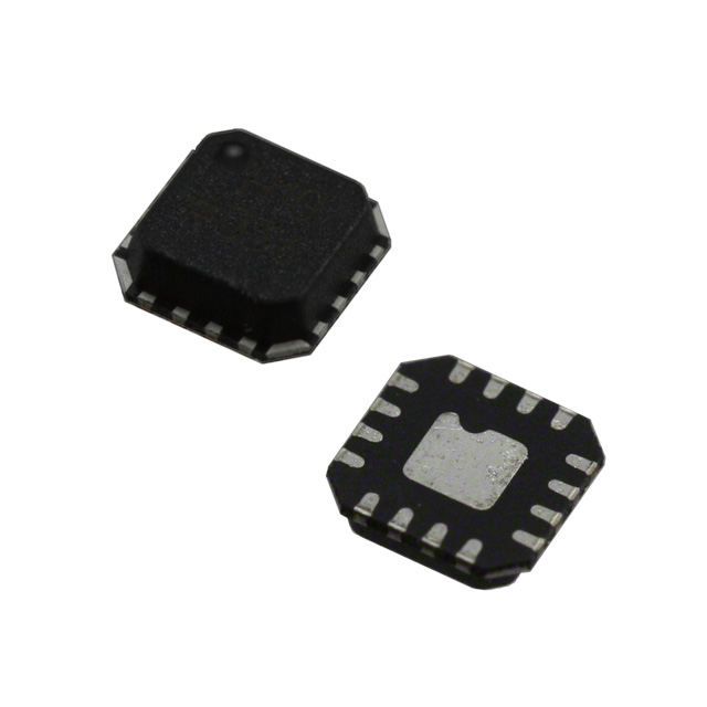
16-lead, 3 mm × 3 mm LFCSP package
APPLICATIONS
Regulation to noise sensitive applications such as RF transceivers, analog-to-digital converter (ADC) and digital-to-analog
converter (DAC) circuits, phase-locked loops (PLLs), voltage
controlled oscillators (VCOs) and clocking integrated circuits
► Field-programmable gate array (FPGA) and digital signal processor (DSP) supplies
► Medical and healthcare
► Industrial and instrumentation
►
Figure 1. Fixed Output Operation
Figure 2. Adjustable Output Operation
GENERAL DESCRIPTION
The ADP1765 is a low noise, low dropout (LDO) linear regulator.
It is designed to operate from a single input supply with an input
voltage as low as 1.10 V without the requirement of an external bias
supply to increase efficiency and provide up to 5 A of output current
(IOUT).
The low 59 mV typical dropout voltage at a 5 A load allows the
ADP1765 to operate with a small headroom while maintaining
regulation and providing better efficiency.
The ADP1765 is optimized for stable operation with small 22 µF
ceramic output capacitors. The ADP1765 delivers optimal transient
performance with minimal printed circuit board (PCB) area.
The ADP1765 is available in fixed output voltages ranging from
0.55 V to 1.5 V. The output voltage (VOUT) of the adjustable output
model can be set from 0.5 V to 1.5 V through an external resistor
connected between VADJ and ground.
The ADP1765 has an externally programmable soft start time by
connecting a capacitor to the SS pin. Short-circuit and thermal
overload protection circuits prevent damage in adverse conditions.
The ADP1765 is available in a small, 16-lead LFCSP package for
the smallest footprint solution to meet a variety of applications.
Rev. B
DOCUMENT FEEDBACK
TECHNICAL SUPPORT
Information furnished by Analog Devices is believed to be accurate and reliable "as is". However, no responsibility is assumed by Analog
Devices for its use, nor for any infringements of patents or other rights of third parties that may result from its use. Specifications subject to
change without notice. No license is granted by implication or otherwise under any patent or patent rights of Analog Devices. Trademarks and
registered trademarks are the property of their respective owners.
�Data Sheet
ADP1765
TABLE OF CONTENTS
Features................................................................ 1
Applications........................................................... 1
Typical Application Circuits....................................1
General Description...............................................1
Specifications........................................................ 3
Input and Output Capacitor: Recommended
Specifications................................................... 4
Absolute Maximum Ratings...................................5
Thermal Data......................................................5
Thermal Resistance/Parameter..........................5
ESD Caution.......................................................5
Pin Configuration and Function Descriptions........ 6
Typical Performance Characteristics..................... 7
Theory of Operation.............................................13
Soft Start Function ...........................................13
Adjustable Output Voltage ...............................14
Enable Feature.................................................14
Power-Good (PG) Feature............................... 14
Applications Information...................................... 16
Capacitor Selection.......................................... 16
Undervoltage Lockout...................................... 17
Current-Limit and Thermal Overload
Protection....................................................... 17
Paralleling ADP1765 Devices for High
Current Applications....................................... 17
Thermal Considerations................................... 18
PCB Layout Considerations............................. 20
Outline Dimensions............................................. 21
Ordering Guide.................................................21
Output Voltage Option...................................... 21
Evaluation Boards............................................ 22
REVISION HISTORY
9/2022—Rev. A to Rev. B
Changes to Table 3.......................................................................................................................................... 5
Changes to Table 5.......................................................................................................................................... 6
Changes to Figure 39.................................................................................................................................... 13
Changes to Adjustable Output Voltage Section............................................................................................. 14
Moved Table 7................................................................................................................................................20
Added Output Voltage Option Section........................................................................................................... 21
analog.com
Rev. B | 2 of 22
�Data Sheet
ADP1765
SPECIFICATIONS
VIN = VOUT + 0.2 V or VIN = 1.1 V, whichever is greater, IOUT = 100 mA, CIN = 22 µF, COUT = 22 µF, CREF = 1 µF, CREG = 1 µF, TA = 25°C,
minimum and maximum limits at TJ = −40°C to +125°C, unless otherwise noted.
Table 1.
Parameter
Symbol
Test Conditions/Comments
Min
INPUT VOLTAGE SUPPLY RANGE
OPERATING SUPPLY CURRENT
VIN
IGND
1.10
SHUTDOWN CURRENT
IGND_SD
TJ = −40°C to +125°C
IOUT = 0 µA
IOUT = 100 mA
IOUT = 5 A
EN = GND
TJ = −40°C to +85°C
TJ = 85°C to 125°C
NOISE1
Output Noise
Noise Spectral Density
POWER SUPPLY REJECTION RATIO1
OUTNOISE
OUTNSD
PSRR
OUTPUT VOLTAGE RANGE
Fixed
Adjustable
FIXED OUTPUT VOLTAGE ACCURACY
VOUT_FIXED
VOUT_ADJ
VOUT
ADJUSTABLE PIN CURRENT
IADJ
ADJUSTABLE OUTPUT VOLTAGE GAIN FACTOR
AD
REGULATION
Line
∆VOUT/∆VIN
Load2
DROPOUT VOLTAGE3
∆VOUT/∆IOUT
VDROPOUT
START-UP TIME1, 4
SOFT START CURRENT
CURRENT-LIMIT THRESHOLD1, 5
tSTARTUP
IREF
ILIMIT
analog.com
5
5
12
4
VIN = VOUT + 0.2 V or VIN = 1.1 V, whichever is
greater, to 1.98 V
IOUT = 100 mA to 5 A
IOUT = 4 A, VOUT = 1.2 V
IOUT = 5 A, VOUT = 1.2 V
CSS = 10 nF, VOUT = 1 V
1.1 V ≤ VIN ≤ 1.98 V
Max
Unit
1.98
17
18
25
V
mA
mA
mA
µA
µA
µA
200
900
10 Hz to 100 kHz, VIN = 1.1 V, VOUT = 0.9 V
100 Hz to 100 kHz, VIN = 1.1 V, VOUT = 0.9 V
10 Hz to 100 kHz, VIN = 1.5 V, VOUT = 1.3 V
100 Hz to 100 kHz, VIN = 1.5 V, VOUT = 1.3 V
10 Hz to 100 kHz, VIN = 1.7 V, VOUT = 1.5 V
100 Hz to 100 kHz, VIN = 1.7 V, VOUT = 1.5 V
VOUT = 0.55 V to 1.5 V, IOUT = 100 mA
At 10 kHz
At 100 kHz
IOUT = 5 A, modulated VIN
10 kHz, VOUT = 1.3 V, VIN = 1.7 V
100 kHz, VOUT = 1.3 V, VIN = 1.7 V
1 MHz, VOUT = 1.3 V, VIN = 1.7 V
10 kHz, VOUT = 0.9 V, VIN = 1.3 V
100 kHz, VOUT = 0.9 V, VIN = 1.3 V
1 MHz, VOUT = 0.9 V, VIN = 1.3 V
TJ = 25°C
IOUT = 100 mA, TJ = 25°C
100 mA < IOUT < 5 A, TJ = 0°C to 85°C
100 mA < IOUT < 5 A, TJ = 0°C to 125°C
TJ = 25°C, VADJ = 0.5 V
VIN = VOUT + 0.2 V or VIN = 1.1 V, whichever is
greater to 1.98 V
VADJ = 0.5 V; VIN = VOUT + 0.2 V or VIN = 1.1 V,
whichever is greater, to 1.98 V
TJ = 25°C
TJ = −40°C to +125°C
Typ
0.55
0.5
−0.75
−1.3
−1.5
49.5
49.0
3
2
3
2
3
2
µV rms
µV rms
µV rms
µV rms
µV rms
µV rms
5
4
nV/√Hz
nV/√Hz
61
43
33
57
43
33
dB
dB
dB
dB
dB
dB
50.0
50.0
1.5
1.5
+0.75
+1.3
+1.5
50.7
51.2
V
V
%
%
%
µA
µA
2.99
2.96
3.02
−0.10
+0.10
%/V
0.3
75
95
%/A
mV
mV
ms
µA
A
8
7.0
0.12
47
59
1
10
8.0
12
8.5
Rev. B | 3 of 22
�Data Sheet
ADP1765
SPECIFICATIONS
Table 1.
Parameter
THERMAL SHUTDOWN1
Threshold
Hysteresis
POWER-GOOD (PG) OUTPUT
Output Voltage Threshold
Falling
Rising
Output Voltage Low
Leakage Current
Delay
PRECISION EN INPUT
Logic Input Voltage
High
Low
Input Logic Hysteresis
Input Leakage Current
Input Delay Time
UNDERVOLTAGE LOCKOUT
Input Voltage
Rising
Falling
Hysteresis
Symbol
Test Conditions/Comments
TSSD
TSSD_HYS
TJ rising
152
16
°C
°C
PGFALL
PGRISE
PGLOW
IPG_LKG
PGDELAY
1.1 V ≤ VIN ≤ 1.98 V
1.1 V ≤ VIN ≤ 1.98 V
1.1 V ≤ VIN ≤ 1.98 V, IPG ≤ 1 mA
1.1 V ≤ VIN ≤ 1.98 V
ENRISING to PGRISING
1.1 V ≤ VIN ≤ 1.98 V
−6.2
−3.5
%
%
V
µA
ms
ENHIGH
ENLOW
ENHYS
IEN_LKG
tEN_DLY
UVLO
UVLORISE
UVLOFALL
UVLOHYS
Min
0.01
0.75
0.60
0.55
VEN = VIN or GND
From EN rising from 0 V to VIN to 0.1 × VOUT
TJ = −40°C to +125°C
TJ = −40°C to +125°C
Typ
0.85
Max
0.3
1
0.65
0.60
50
0.01
100
0.69
0.65
1.00
0.93
70
1.06
1
Unit
V
V
mV
µA
µs
V
V
mV
1
Guaranteed by characterization but not production tested.
2
Based on an endpoint calculation using 100 mA and 5 A loads.
3
Dropout voltage is defined as the input-to-output voltage differential when the input voltage is set to the nominal output voltage, which applies only for output voltages above
1.1 V.
4
Start-up time is the time from the rising edge of VEN to VOUT being at 90% of its nominal value.
5
Current-limit threshold is the current at which the output voltage drops to 90% of the specified typical value. For example, the current limit for a 1.0 V output voltage is
defined as the current that causes the output voltage to drop to 90% of 1.0 V, or 0.9 V.
INPUT AND OUTPUT CAPACITOR: RECOMMENDED SPECIFICATIONS
Table 2.
Parameter
Symbol
CAPACITANCE1
Input
Output
Regulator
Reference
CAPACITOR EQUIVALENT SERIES RESISTANCE (ESR)
CIN, COUT
CREG
CREF
1
Test Conditions/Comments
Min
Typ
14.5
14.5
0.7
0.07
22
22
1
1
Max
Unit
TA = −40°C to +125°C
CIN
COUT
CREG
CREF
RESR
µF
µF
µF
µF
TA = −40°C to +125°C
0.2
0.5
2
Ω
Ω
Ω
The minimum input and output capacitance must be >14.5 µF over the full range of the operating conditions. Consider the full range of the operating conditions in the
application during device selection to ensure that the minimum capacitance specification is met. X7R and X5R type capacitors are recommended. Y5V and Z5U capacitors
are not recommended for use with any LDO.
analog.com
Rev. B | 4 of 22
�Data Sheet
ADP1765
ABSOLUTE MAXIMUM RATINGS
Table 3.
Parameter
Rating
VIN to GND
EN to GND
VOUT to GND
SENSE to GND
VREG to GND
REFCAP to GND
VADJ to GND
SS to GND
PG to GND
Storage Temperature Range
Operating Junction Temperature Range
Junction Temperature
Lead Temperature (Soldering, 10 sec)
−0.3 V to +2.16 V
−0.3 V to +3.96 V
−0.3 V to VIN
−0.3 V to VIN
−0.3 V to VIN
−0.3 V to VIN
−0.3 V to VIN
−0.3 V to VIN
−0.3 V to +3.96 V
−65°C to +150°C
−40°C to +125°C
150°C
300°C
Stresses at or above those listed under Absolute Maximum Ratings
may cause permanent damage to the product. This is a stress
rating only; functional operation of the product at these or any other
conditions above those indicated in the operational section of this
specification is not implied. Operation beyond the maximum operating conditions for extended periods may affect product reliability.
THERMAL DATA
Absolute maximum ratings apply individually only, not in combination. The ADP1765 can be damaged when the junction temperature
limits are exceeded. The use of appropriate thermal management
techniques is recommended to ensure that the maximum junction
temperature does not exceed the limits shown in Table 3.
tion to ambient thermal resistance measured in a one cubic foot
sealed enclosure. θJC is the junction to case thermal resistance. θJB
is the junction to board thermal resistance. ΨJB is the junction to
board thermal characterization parameter. ΨJT is the junction to top
thermal characterization parameter.
In applications where high maximum power dissipation exists,
close attention to thermal board design is required. Thermal resistance/parameter values may vary, depending on the PCB material,
layout, and environmental conditions.
Table 4. Thermal Resistance/Parameter
Package Type
θJA
θJC
θJB
ΨJB
ΨJT
Unit
CP-16-481
40.65
7.47
17.38
12.9
0.85
°C/W
1
Thermal resistance/parameter simulated values are based on a JEDEC 2S2P
thermal test board for ΨJT, ΨJB, θJA, and θJB and a JEDEC 1S0P thermal test
board for θJC with four thermal vias. See JEDEC JESD51-12.
ESD CAUTION
ESD (electrostatic discharge) sensitive device. Charged devices and circuit boards can discharge without detection. Although
this product features patented or proprietary protection circuitry,
damage may occur on devices subjected to high energy ESD.
Therefore, proper ESD precautions should be taken to avoid
performance degradation or loss of functionality.
Use the following equation to calculate the junction temperature
(TJ) from the board temperature (TBOARD) or package top temperature (TTOP)
TJ = TBOARD + (PD × ΨJB)
TJ = TTOP + (PD × ΨJT)
ΨJB is the junction to board thermal characterization parameter and
ΨJT is the junction to top thermal characterization parameter with
units of °C/W.
ΨJB of the package is based on modeling and calculation using
a 4-layer board. JESD51-12, Guidelines for Reporting and Using
Electronic Package Thermal Information, states that thermal characterization parameters are not the same as thermal resistances.
ΨJB measures the component power flowing through multiple thermal paths rather than a single path as in thermal resistance, θJB.
Therefore, ΨJB thermal paths include convection from the top of the
package as well as radiation from the package, factors that make
ΨJB more useful in real-world applications.
THERMAL RESISTANCE/PARAMETER
Values shown in Table 4 are calculated in compliance with JEDEC
standards for thermal reporting. θJA is the natural convection juncanalog.com
Rev. B | 5 of 22
�Data Sheet
ADP1765
PIN CONFIGURATION AND FUNCTION DESCRIPTIONS
Figure 3. Pin Configuration
Table 5. Pin Function Descriptions
Pin No.
Mnemonic
Description
1 to 4
VIN
5
6
REFCAP
VREG
7
8
GND
VADJ
9 to 12
VOUT
13
SENSE
14
15
SS
PG
16
EN
Regulator Input Supply. Bypass VIN to GND with a 22 µF or greater capacitor. Note that all four VIN pins must be connected to the source
supply.
Reference Filter Capacitor. Connect a 1 µF capacitor from the REFCAP pin to ground. Do not connect a load from this pin to ground.
Regulated Input Supply to LDO Amplifier. Bypass VREG to GND with a 1 µF or greater capacitor. Do not connect a load from this pin to
ground.
Ground.
Adjustable Voltage Pin for the Adjustable Output Option. Connect a 10 kΩ external resistor between the VADJ pin and ground to set the output
voltage to 1.5 V. Due to an internal low-pass filter, externally modifying the VADJ pin does not cause an instantaneous change in the output
voltage. Only connect this pin to a resistor to ground. For the fixed output option, leave this pin floating.
Regulated Output Voltage. Bypass VOUT to GND with a 22 µF or greater capacitor. Note that all four VOUT pins must be connected to the
load.
Sense Input. The SENSE pin measures the actual output voltage at the load and feeds it to the error amplifier. Connect SENSE as close to the
load as possible to minimize the effect of IR drop between VOUT and the load. Do not connect an external resistor divider network on SENSE.
Soft Start Pin. A capacitor connected to this pin determines the soft start time.
Power-Good Output. This open-drain output requires an external pull-up resistor. If the device is in shutdown mode, current-limit mode, or
thermal shutdown mode, or if the VOUT voltage falls below 90% of the nominal output voltage, the PG pin immediately transitions to low.
Enable Input. Drive the EN pin high to turn on the regulator. Drive the EN pin low to turn off the regulator. For automatic startup, connect the
EN pin to the VIN pin.
Exposed Pad. The exposed pad is electrically connected to GND. It is recommended that this pad be connected to a ground plane on the
PCB. The exposed pad is on the bottom of the package.
EP
analog.com
Rev. B | 6 of 22
�Data Sheet
ADP1765
TYPICAL PERFORMANCE CHARACTERISTICS
VIN = VOUT + 0.2 V or VIN = 1.1 V, whichever is greater, VOUT = 1.3 V, IOUT = 100 mA, TA = 25°C, unless otherwise noted.
Figure 4. Output Voltage (VOUT) vs. Temperature, VOUT = 1.3 V
Figure 7. Ground Current (IGND) vs. Temperature, VOUT = 1.3 V
Figure 5. Output Voltage (VOUT) vs. Load Current (ILOAD), VOUT = 1.3 V
Figure 8. Ground Current (IGND) vs. Load Current (ILOAD), VOUT = 1.3 V
Figure 6. Output Voltage (VOUT) vs. Input Voltage (VIN), VOUT = 1.3 V
Figure 9. Ground Current (IGND) vs. Input Voltage (VIN), VOUT = 1.3 V
analog.com
Rev. B | 7 of 22
�Data Sheet
ADP1765
TYPICAL PERFORMANCE CHARACTERISTICS
Figure 10. Output Voltage (VOUT) vs. Temperature, VOUT = 0.9 V
Figure 13. Ground Current (IGND) vs. Temperature, VOUT = 0.9 V
Figure 11. Output Voltage (VOUT) vs. Load Current (ILOAD), VOUT = 0.9 V
Figure 14. Ground Current (IGND) vs. Load Current (ILOAD), VOUT = 0.9 V
Figure 12. Output Voltage (VOUT) vs. Input Voltage (VIN), VOUT = 0.9 V
Figure 15. Ground Current (IGND) vs. Input Voltage (VIN), VOUT = 0.9 V
analog.com
Rev. B | 8 of 22
�Data Sheet
ADP1765
TYPICAL PERFORMANCE CHARACTERISTICS
Figure 16. Shutdown Current (IGND_SD) vs. Temperature at Various Input
Voltages (VIN), VOUT = 0.9 V
Figure 19. Ground Current (IGND) vs. Input Voltage (VIN) in Dropout, VOUT = 1.3
V
Figure 17. Dropout Voltage (VDROPOUT) vs. Load Current (ILOAD), VOUT = 1.3 V
Figure 20. Load Transient Response, COUT = 22 µF, VIN = 1.8 V, VOUT = 1.3 V
Figure 18. Output Voltage (VOUT) vs. Input Voltage (VIN) in Dropout, VOUT = 1.3
V
Figure 21. Load Transient Response, COUT = 47 µF, VIN = 1.8 V, VOUT = 1.3 V
analog.com
Rev. B | 9 of 22
�Data Sheet
ADP1765
TYPICAL PERFORMANCE CHARACTERISTICS
Figure 22. Load Transient Response, COUT = 22 µF, VIN = 1.4 V, VOUT = 0.9 V
Figure 23. Load Transient Response, COUT = 47 µF, VIN = 1.4 V, VOUT = 0.9 V
Figure 24. Line Transient Response, Load Current = 5 A, VIN = 1.6 V to 1.98 V
Step, VOUT = 1.3 V
analog.com
Figure 25. Line Transient Response, Load Current = 5 A, VIN = 1.3 V to 1.7 V
Step, VOUT = 0.9 V
Figure 26. Output Noise vs. Load Current (ILOAD)
Figure 27. Output Noise vs. Output Voltage (VOUT)
Rev. B | 10 of 22
�Data Sheet
ADP1765
TYPICAL PERFORMANCE CHARACTERISTICS
Figure 28. Noise Spectral Density vs. Frequency at Various Output Voltages
(VOUT), 0.1 Hz to 1 MHz
Figure 31. Noise Spectral Density vs. Frequency at Various Load Current
(IOUT), 10 Hz to 10 MHz
Figure 29. Noise Spectral Density vs. Frequency at Various Output Voltages
(VOUT), 10 Hz to 10 MHz
Figure 32. Power Supply Rejection Ratio (PSRR) vs. Frequency at Various
Input Voltages (VIN), VOUT = 1.3 V, Load = 5 A
Figure 30. Noise Spectral Density vs. Frequency at Various Load Current
(IOUT), 0.1 Hz to 1 MHz
Figure 33. Power Supply Rejection Ratio (PSRR) vs. Frequency at Various
Loads (ILOAD), VOUT = 1.3 V, VIN = 1.7 V
analog.com
Rev. B | 11 of 22
�Data Sheet
ADP1765
TYPICAL PERFORMANCE CHARACTERISTICS
Figure 34. Power Supply Rejection Ratio (PSRR) vs. Frequency at Various
Input Voltages (VIN), VOUT = 0.9 V, Load = 5 A
Figure 36. Power Supply Rejection Ratio (PSRR) vs. Headroom Voltage at
Various Frequencies, VOUT = 0.9 V, Load = 5 A
Figure 35. Power Supply Rejection Ratio (PSRR) vs. Frequency at Various
Loads (ILOAD), VOUT = 0.9 V, VIN = 1.3 V
Figure 37. Power Supply Rejection Ratio (PSRR) vs. Headroom Voltage at
Various Frequencies, VOUT = 1.3 V, Load = 5 A
analog.com
Rev. B | 12 of 22
�Data Sheet
ADP1765
THEORY OF OPERATION
The ADP1765 is a low dropout (LDO), low noise linear regulator
that uses an advanced proprietary architecture to achieve high
efficiency regulation. It also provides high PSRR and excellent line
and load transient response using a small 22 μF ceramic output
capacitor. The device operates from a 1.10 V to 1.98 V input rail to
provide up to 5 A of output current. The supply current in shutdown
mode is less than 4 µA.
Figure 38. Functional Block Diagram, Fixed Output
the EN pin to enable and disable the VOUT pin under normal
operating conditions. When EN is high, VOUT turns on. When EN is
low, VOUT turns off. For automatic startup, tie EN to VIN.
SOFT START FUNCTION
For applications that require a controlled startup, the ADP1765
provides a programmable soft start function. The programmable
soft start is useful for reducing inrush current upon startup and
for providing voltage sequencing. To implement soft start, connect
a small ceramic capacitor from SS to GND. At startup, a 10 µA
current source charges this capacitor. The voltage at SS limits the
ADP1765 start-up output voltage, providing a smooth ramp up to
the nominal output voltage. To calculate the start-up time for the
fixed output (tSTARTUP_FIXED) and adjustable (tSTARTUP_ADJ) output,
use the following equations:
tSTARTUP_FIXED = tDELAY + VREF × (CSS/ISS)
(1)
tSTARTUP_ADJ = tDELAY + VADJ × (CSS/ISS)
(2)
where:
tDELAY is a fixed delay of 100 µs.
VREF is a 0.5 V internal reference for the fixed output model option.
CSS is the soft start capacitance from SS to GND.
ISS is the current sourced from SS (10 µA).
VADJ is the voltage at the VADJ pin, equal to RADJ × IADJ.
Figure 39. Functional Block Diagram, Adjustable Output
Internally, the ADP1765 consists of a reference, an error amplifier,
and a pass device. The output current is delivered via the pass
device, which is controlled by the error amplifier, forming a negative feedback system that ideally drives the feedback voltage to
equal the reference voltage. If the feedback voltage is lower than
the reference voltage, the negative feedback drives more current,
increasing the output voltage. If the feedback voltage is higher than
the reference voltage, the negative feedback drives less current,
decreasing the output voltage.
Figure 40. Fixed VOUT Ramp-Up with External Soft Start Capacitor (VOUT, EN)
vs. Time
The ADP1765 is available in output voltages ranging from 0.55 V
to 1.5 V for a fixed output. Contact your local Analog Devices, Inc.,
sales representative for other fixed voltage options. The adjustable
output option can be set from 0.5 V to 1.5 V. The ADP1765 uses
analog.com
Rev. B | 13 of 22
�Data Sheet
ADP1765
THEORY OF OPERATION
Figure 42. Typical EN Pin Operation
Figure 41. Adjustable VOUT Ramp-Up with External Soft Start Capacitor
(VOUT, EN) vs. Time
ADJUSTABLE OUTPUT VOLTAGE
The output voltage of the ADP1765 can be set over a 0.5 V to 1.5 V
range. Connect a resistor (RADJ) from the VADJ pin to ground to set
the output voltage. To calculate the output voltage (VOUT), use the
following equation:
VOUT = AD × (RADJ × IADJ)
As shown in Figure 43, the EN pin has built in hysteresis. This
hysteresis prevents on/off oscillations that can occur due to noise
on the EN pin as it passes through the threshold points.
(3)
where:
AD is the gain factor with a typical value of 2.99 between the VADJ
pin and VOUT pin.
IADJ is the 50 µA constant current out of the VADJ pin.
Due to an internal low-pass filter, externally modifying the VADJ
pin does not cause an instantaneous change in the output voltage.
For normal operation, it is recommended to only connect a resistor
across VADJ to ground.
ENABLE FEATURE
The ADP1765 uses the EN pin to enable and disable the VOUT
pins under normal operating conditions. As shown in Figure 42,
when a rising voltage on EN crosses the active threshold, VOUT
turns on. When a falling voltage on EN crosses the inactive threshold, VOUT turns off.
Figure 43. Output Voltage (VOUT) vs. EN Threshold, VOUT = 1.3 V
POWER-GOOD (PG) FEATURE
The ADP1765 provides a power-good pin (PG) to indicate the
status of the output. This open-drain output requires an external
pull-up resistor that can be connected to VIN or VOUT. If the device
is in shutdown mode, current-limit mode, or thermal shutdown, or
if it falls below 90% of the nominal output voltage, PG immediately
transitions low. During soft start, the rising threshold of the powergood signal is 96.5% of the nominal output voltage.
The open-drain output is held low when the ADP1765 has sufficient
input voltage to turn on the internal PG transistor. An optional soft
start delay can be detected. The PG transistor is terminated via a
pull-up resistor to VIN or VOUT.
Power-good accuracy is 93.8% of the nominal regulator output
voltage when this voltage is rising, with a 96.5% trip point when this
voltage is falling.
analog.com
Rev. B | 14 of 22
�Data Sheet
ADP1765
THEORY OF OPERATION
Regulator input voltage brownouts or glitches trigger a power no
good if VOUT falls below 93.8%.
A normal power-down triggers a power good when VOUT is at
96.5%.
Figure 44. Typical PG Voltage Behavior vs. VOUT, VIN Rising (VOUT = 1.3 V)
Figure 45. Typical PG Voltage Behavior vs. VOUT, VIN Falling (VOUT = 1.3 V)
analog.com
Rev. B | 15 of 22
�Data Sheet
ADP1765
APPLICATIONS INFORMATION
CAPACITOR SELECTION
Output Capacitor
The ADP1765 is designed for operation with small, space-saving
ceramic capacitors, but it can function with most commonly used
capacitors as long as care is taken with the effective series resistance (ESR) value. The ESR of the output capacitor affects the
stability of the LDO control loop. A minimum of 22 µF capacitance
with an ESR of 50 mΩ or less is recommended to ensure the
stability of the ADP1765. Transient response to changes in load
current is also affected by output capacitance. Using a larger
value of output capacitance improves the transient response of the
ADP1765 to large changes in load current. Figure 46 and Figure 47
show the transient responses for output capacitance values of 22
µF and 47 µF, respectively.
are encountered. If an output capacitance greater than 22 µF is
required, it is recommended to increase the input capacitor to
match it.
Input and Output Capacitor Properties
Use any good quality ceramic capacitors with the ADP1765 as
long as they meet the minimum capacitance and maximum ESR
requirements. Ceramic capacitors are manufactured with a variety
of dielectrics, each with different behavior over temperature and
applied voltage. Capacitors must have a dielectric adequate to
ensure the minimum capacitance over the necessary temperature
range and dc bias conditions. X5R or X7R dielectrics with a voltage
rating of 6.3 V or 10 V are recommended. Y5V and Z5U dielectrics
are not recommended, due to their poor temperature and dc bias
characteristics.
Figure 48 shows the capacitance vs. dc bias voltage characteristics
of a C2012X5R1A226K125AB, 0805 case, 22 µF, 10 V, X5R capacitor. The voltage stability of a capacitor is strongly influenced by the
capacitor size and voltage rating. In general, a capacitor in a larger
package or with a higher voltage rating exhibits improved stability.
The temperature variation of the X5R dielectric is about ±15% over
the −55°C to +85°C temperature range and is not a function of
package size or voltage rating.
Figure 46. Output Transient Response, COUT = 22 µF, VOUT = 1.3 V
Figure 48. Capacitance vs. DC Bias Voltage
Use Equation 4 to determine the worst-case capacitance, accounting for capacitor variation over temperature, component tolerance,
and voltage.
CEFF = COUT × (1 − TEMPCO) × (1 − TOL)
Figure 47. Output Transient Response, COUT = 47 µF, VOUT = 1.3 V
Input Bypass Capacitor
Connecting a 22 µF capacitor from the VIN pin to the GND pin
to the ground plane reduces the circuit sensitivity to the PCB layout, especially when long input traces or high source impedances
analog.com
(4)
where:
CEFF is the effective capacitance at the operating voltage.
COUT is the output capacitor.
TEMPCO is the worst case capacitor temperature coefficient.
TOL is the worst case component tolerance.
In this example, the worst case temperature coefficient (TEMPCO)
over −55°C to +125°C is assumed to be 15% for an X5R dielectric.
Rev. B | 16 of 22
�Data Sheet
ADP1765
APPLICATIONS INFORMATION
The tolerance of the capacitor (TOL) is assumed to be 10%, and
COUT = 19.48 µF at 1.0 V, as shown in Figure 48.
Substituting these values in Equation 4 yields
CEFF = 19.48 μF × (1 − 0.15) × (1 − 0.1) = 14.9 μF
Therefore, the capacitor chosen in this example meets the minimum capacitance requirement of the LDO over temperature and
tolerance at the chosen output voltage.
To guarantee the performance of the ADP1765, it is imperative to
evaluate the effects of dc bias, temperature, and tolerances on the
behavior of the capacitors for each application.
shutdown activates, turning off the output and reducing the output
current to zero. As the junction temperature cools and drops below
136°C, the output turns on and conducts 8.0 A into the short, again
causing the junction temperature to rise above 152°C. This thermal
oscillation between 136°C and 152°C causes a current oscillation
between 8.0 A and 0 A that continues as long as the short remains
at the output.
Current-limit and thermal overload protections are intended to protect the device against accidental overload conditions. For reliable
operation, device power dissipation must be externally limited so
that junction temperatures do not exceed 125°C.
UNDERVOLTAGE LOCKOUT
PARALLELING ADP1765 DEVICES FOR HIGH
CURRENT APPLICATIONS
The ADP1765 has an internal undervoltage lockout (UVLO) circuit
that disables all inputs and the output when the input voltage is less
than approximately 1.06 V. The UVLO ensures that the ADP1765
inputs and output behave in a predictable manner during power-up.
In applications where high output current is required while maintaining low noise and high PSRR performance, connect two ADP1765
devices in parallel to handle loads up to 9 A.
CURRENT-LIMIT AND THERMAL OVERLOAD
PROTECTION
The ADP1765 is protected against damage due to excessive power
dissipation by current-limit and thermal overload protection circuits.
The ADP1765 is designed to reach the current limit when the output
load reaches 8.0 A (typical). When the output load exceeds 8.0 A,
the output voltage is reduced to maintain a constant current limit.
Thermal overload protection is included that limits the junction
temperature to a maximum of 152°C (typical). Under extreme
conditions (that is, high ambient temperature and power dissipation)
when the junction temperature begins to rise above 152°C, the
output turns off, reducing the output current to zero. When the
junction temperature drops below 136°C (typical), the output turns
on again, and the output current is restored to its nominal value.
Consider the case where a hard short from VOUT to ground occurs.
At first, the ADP1765 reaches the current limit so that only 8.0 A
is conducted into the short. If self-heating of the junction becomes
great enough to cause its temperature to rise above 152°C, thermal
analog.com
When paralleling the ADP1765, the two outputs must be of the
same voltage setting to maintain good current sharing between
the two LDOs. To improve current sharing accuracy, add identical
ballast resistors (RBALLAST) at the output of each regulator, as
shown in Figure 49. Note that large ballast resistors improve current
sharing accuracy, but degrade the load regulation performance and
increase the losses along the power line. Therefore, it is best to
keep the ballast resistors at a minimum. In addition, tie the VADJ,
SS, and REFCAP pins of the LDO regulators together to minimize
error between the two outputs.
Use Equation 5 to calculate the output of the two paralleled
ADP1765 LDOs.
VOUT = 2 × AD × (RADJ × IADJ)
(5)
where:
AD is the gain factor with a typical value of 2.99 between the VADJ
pin and VOUT pin.
IADJ is the 50 µA constant current out of the VADJ pin.
Rev. B | 17 of 22
�Data Sheet
ADP1765
APPLICATIONS INFORMATION
Figure 49. Two ADP1765 Devices Connected in Parallel to Achieve Higher Current Output
THERMAL CONSIDERATIONS
In applications with a low input-to-output voltage differential, the
ADP1765 does not dissipate much heat. However, in applications
with high ambient temperature and/or high input voltage, the heat
dissipated in the package may become large enough to cause the
junction temperature of the die to exceed the maximum junction
temperature of 125°C.
When the junction temperature exceeds 152°C, the regulator enters
thermal shutdown. The regulator recovers only after the junction
temperature decreases below 136°C to prevent any permanent
damage. Therefore, thermal analysis for the chosen application is
important to guarantee reliable performance over all conditions. The
junction temperature of the die is the sum of the board temperature
and the temperature rise of the package due to the power dissipation, as shown in Equation 6.
To guarantee reliable operation, the junction temperature of the
ADP1765 must not exceed 125°C. To ensure that the junction temperature stays below this maximum value, the user must be aware
of the parameters that contribute to junction temperature changes.
These parameters include board temperature, power dissipation in
the power device, and thermal characterization parameter between
the junction and board (ΨJB). The ΨJB parameter is dependent on
the package assembly compounds and the PCB copper area. Table
6 shows the typical ΨJB values for the 16-lead LFCSP package for
various PCB copper areas.
where:
TB is the board temperature.
PD is the power dissipation in the die, given by
PD = ((VIN − VOUT) × ILOAD) + (VIN × IGND)
(7)
where:
VIN and VOUT are the input and output voltages, respectively.
ILOAD is the load current.
IGND is the ground current.
Power dissipation due to ground current is quite small and can be
ignored. Therefore, the junction temperature equation simplifies to
TJ = TB + (((VIN − VOUT) × ILOAD) × ΨJB)
(8)
As shown in Equation 8, for a given board temperature, input-tooutput voltage differential and continuous load current, a minimum
copper area requirement exists for the PCB to ensure that the
junction temperature does not rise above 125°C.
Figure 50 to Figure 55 show the junction temperature calculations
for the different board temperatures, power dissipation, and areas
of the PCB copper.
Table 6. Typical non-JEDEC ΨJB Values
PCB Copper Area (mm2)
ΨJB (°C/W) at 2W
25
100
500
1000
71.05
18.9
13.45
13.15
Calculate the junction temperatures of the ADP1765 by
TJ = TB + (PD × ΨJB)
analog.com
(6)
Figure 50. 1000 mm2 of PCB Copper, TB = 25°C
Rev. B | 18 of 22
�Data Sheet
ADP1765
APPLICATIONS INFORMATION
Figure 51. 500 mm2 of PCB Copper, TB = 25°C
Figure 54. 500 mm2 of PCB Copper, TB = 50°C
Figure 52. 100 mm2 of PCB Copper, TB= 25°C
Figure 55. 100 mm2 of PCB Copper, TB = 50°C
Figure 53. 1000 mm2 of PCB Copper, TB = 50°C
Figure 56. Thermal Image of the ADP1765 Evaluation Board at ILOAD = 5 A,
VIN = 1.5 V, VOUT = 1.3 V, TB = 93.3°C
Figure 56 shows a thermal image of the ADP1765 evaluation
board operating at a 5 A current load. The total power dissipation
on the ADP1765 is 933 mW, which makes the temperature on
analog.com
Rev. B | 19 of 22
�Data Sheet
ADP1765
APPLICATIONS INFORMATION
the surface of the device higher by 22°C than the temperature of
the evaluation board.
PCB LAYOUT CONSIDERATIONS
Place the input capacitor as close as possible to the VIN and GND
pins. Place the output capacitor as close as possible to the VOUT
and GND pins. Place the soft start capacitor (CSS) as close as
possible to the SS pin. Place the reference capacitor (CREF) and
regulator capacitor (CREG) as close as possible to the REFCAP pin
and VREG pin, respectively. Connect the load as close as possible
to the VOUT and SENSE pins.
Figure 59. Typical Board Layout, Bottom Side
Table 7. Related Devices
Model
ADP1761
ADP1762
ADP1763
Figure 57. Evaluation Board
ADP1740/
ADP1741
ADP1752/
ADP1753
ADP1754/
ADP1755
Input
Voltage
Maximum
Current
Fixed/Adjustable Package
1.10 V to
1.98 V
1.10 V to
1.98 V
1.10 V to
1.98 V
1.6 V to 3.6 V
1A
Fixed/adjustable
16-lead LFCSP
2A
Fixed/adjustable
16-lead LFCSP
3A
Fixed/adjustable
16-lead LFCSP
2A
Fixed/adjustable
16-lead LFCSP
1.6 V to 3.6 V 0.8 A
Fixed/adjustable
16-lead LFCSP
1.6 V to 3.6 V 1.2 A
Fixed/adjustable
16-lead LFCSP
Figure 58. Typical Board Layout, Top Side
analog.com
Rev. B | 20 of 22
�Data Sheet
ADP1765
OUTLINE DIMENSIONS
Figure 60. 16-Lead Lead Frame Chip Scale Package [LFCSP]
3 mm × 3 mm Body and 0.75 mm Package Height
(CP-16-48)
Dimensions shown in millimeters
Updated: August 30, 2022
ORDERING GUIDE
Model1
Temperature Range
Package Description
Packing Quantity
Package
Option
Marking
Code
ADP1765ACPZ0.85-R7
ADP1765ACPZ0.95-R7
ADP1765ACPZ-0.9-R7
ADP1765ACPZ-1.0-R7
ADP1765ACPZ-1.1-R7
ADP1765ACPZ1.25-R7
ADP1765ACPZ-1.2-R7
ADP1765ACPZ-1.3-R7
ADP1765ACPZ-1.5-R7
ADP1765ACPZ-R7
−40°C to +125°C
−40°C to +125°C
−40°C to +125°C
−40°C to +125°C
−40°C to +125°C
−40°C to +125°C
−40°C to +125°C
−40°C to +125°C
−40°C to +125°C
−40°C to +125°C
16-Lead LFCSP (3mm x 3mm x 0.75mm w/ EP)
16-Lead LFCSP (3mm x 3mm x 0.75mm w/ EP)
16-Lead LFCSP (3mm x 3mm x 0.75mm w/ EP)
16-Lead LFCSP (3mm x 3mm x 0.75mm w/ EP)
16-Lead LFCSP (3mm x 3mm x 0.75mm w/ EP)
16-Lead LFCSP (3mm x 3mm x 0.75mm w/ EP)
16-Lead LFCSP (3mm x 3mm x 0.75mm w/ EP)
16-Lead LFCSP (3mm x 3mm x 0.75mm w/ EP)
16-Lead LFCSP (3mm x 3mm x 0.75mm w/ EP)
16-Lead LFCSP (3mm x 3mm x 0.75mm w/ EP)
Reel, 1500
Reel, 1500
Reel, 1500
Reel, 1500
Reel, 1500
Reel, 1500
Reel, 1500
Reel, 1500
Reel, 1500
Reel, 1500
CP-16-48
CP-16-48
CP-16-48
CP-16-48
CP-16-48
CP-16-48
CP-16-48
CP-16-48
CP-16-48
CP-16-48
LUA
LUM
LUB
LUD
LUE
LUR
LUF
LUG
LUJ
LUK
1
Z = RoHS Compliant Part.
OUTPUT VOLTAGE OPTION
Model1
Output Voltage (V)2
ADP1765ACPZ0.85-R7
ADP1765ACPZ-0.9-R7
ADP1765ACPZ0.95-R7
ADP1765ACPZ-1.0-R7
ADP1765ACPZ-1.1-R7
ADP1765ACPZ-1.2-R7
ADP1765ACPZ1.25-R7
ADP1765ACPZ-1.3-R7
ADP1765ACPZ-1.5-R7
ADP1765ACPZ-R7
0.85
0.9
0.95
1.0
1.1
1.2
1.25
1.3
1.5
Adjustable
1
Z = RoHS Compliant Part.
2
For additional voltage options, contact a local Analog Devices sales or distribution representative. Additional voltage options are available by special order and include the
following: 0.55 V, 0.6 V, 0.65 V, 0.7 V, 0.75 V, 0.8 V, 1.05 V, 1.15 V, 1.35 V, 1.4 V, and 1.45 V.
analog.com
Rev. B | 21 of 22
�Data Sheet
ADP1765
OUTLINE DIMENSIONS
EVALUATION BOARDS
Model1
Description
ADP1765-1.0-EVALZ
ADP1765-ADJ-EVALZ
Evaluation Board (Fixed)
Evaluation Board (Adjustable)
1
Z = RoHS Compliant Part.
©2017-2022 Analog Devices, Inc. All rights reserved. Trademarks and
registered trademarks are the property of their respective owners.
One Analog Way, Wilmington, MA 01887-2356, U.S.A.
Rev. B | 22 of 22
�