Evaluation Board for ADP2118
EVAL-ADP2118
GENERAL DESCRIPTION
PRODUCT DESCRIPTION
The evaluation (demo) board provides an easy way to evaluate
the ADP2118 buck regulator. This data sheet describes how to
quickly set up the board to begin collecting performance data. Full
details on the ADP2118 are available in the ADP2118 data
sheet, which is available from Analog Devices, Inc., and should
be consulted in conjunction with this data sheet when using the
evaluation board.
The ADP2118 is a low quiescent current, synchronous,
step-down, dc-to-dc regulator in a compact 4 mm × 4 mm
LFCSP_WQ package. It uses a current mode, constant frequency pulse width modulation (PWM) control scheme for
excellent stability and transient response. Under light loads,
the ADP2118 can be configured to operate in pulse frequency
modulation (PFM) mode that reduces switching frequency to
save power.
This data sheet also describes the design process for the
ADP2118 buck regulator, including external component
selection, and how to obtain the best dynamic performance.
The ADP2118 runs from input voltages of 2.3 V to 5.5 V. The
ADP2118 requires minimal external parts and provides a high
efficiency solution with its integrated power switch, synchronous rectifier, and internal compensation. Other key features
include undervoltage lockout (UVLO), integrated soft start to
limit inrush current at startup, overvoltage protection (OVP),
overcurrent protection (OCP), and thermal shutdown (TSD).
Thermal performance is described, which provides a current
derating reference for the user when the ADP2118 is operating
at different ambient temperatures.
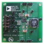
08742-001
ADP2118 EVALUATION BOARD
Figure 1.
Rev. 0
Evaluation boards are only intended for device evaluation and not for production purposes.
Evaluation boards are supplied “as is” and without warranties of any kind, express, implied, or
statutory including, but not limited to, any implied warranty of merchantability or fitness for a
particular purpose. No license is granted by implication or otherwise under any patents or other
intellectual property by application or use of evaluation boards. Information furnished by Analog
Devices is believed to be accurate and reliable. However, no responsibility is assumed by Analog
Devices for its use, nor for any infringements of patents or other rights of third parties that may result
from its use. Analog Devices reserves the right to change devices or specifications at any time
without notice. Trademarks and registered trademarks are the property of their respective owners.
Evaluation boards are not authorized to be used in life support devices or systems.
One Technology Way, P.O. Box 9106, Norwood, MA 02062-9106, U.S.A.
www.analog.com
Tel: 781.329.4700
Fax: 781.461.3113
©2010 Analog Devices, Inc. All rights reserved.
�EVAL-ADP2118
TABLE OF CONTENTS
General Description ......................................................................... 1
Performance Improvement ..........................................................7
Product Description ......................................................................... 1
Layout Guidelines..........................................................................9
ADP2118 Evaluation Board ............................................................ 1
Thermal Performance .................................................................... 10
Revision History ............................................................................... 2
Evaluation Board Schematic and Artwork.................................. 11
Evaluation Board Hardware ............................................................ 3
Evaluation Board Layout ........................................................... 12
Powering Up the evaluation Board ............................................ 3
Ordering Information .................................................................... 14
Measuring Evaulation Board Performance ............................... 4
Ordering Guide .......................................................................... 14
ADP2118 Design Process ................................................................ 5
ESD Caution................................................................................ 14
External Component Selection ................................................... 5
REVISION HISTORY
1/10—Revision 0: Initial Version
Rev. 0 | Page 2 of 16
�EVAL-ADP2118
EVALUATION BOARD HARDWARE
Output Load Connection
POWERING UP THE EVALUATION BOARD
The ADP2118 evaluation board is fully assembled and tested.
Before applying power to the evaluation board, follow the setup
procedures in this section.
Jumper Settings
Refer to Table 1 for selecting the jumper positions.
Make sure the enable input, EN, is high.
If an ammeter is used, connect it in series with the load;
connect the positive (+) ammeter terminal to the evaluation
board VOUT terminal (J9), the negative (−) ammeter terminal
to the positive (+) load terminal, and the negative (−) load
terminal to the evaluation board GND terminal (J12).
Table 1. Jumper Settings
Jumper
J2 (EN)
J4
(SYNC/MODE)
J7 (FREQ)
States
High
Low
High
Low
External
clock
High
Low
J10 (TRK)
High
External
voltage
Make sure that the board is turned off before connecting the
load. If the load includes an ammeter, or if the current is not
measured, connect the load directly to the evaluation board
with the positive (+) load connection to the VOUT terminal
(J9) and negative (−) load connection to the GND terminal
(J12).
Function
Enable VOUT
Disable VOUT
Force PWM
Enable PFM
Synchronize to the external clock
Input and Output Voltmeter Connections
fS = 1.2 MHz
180° out of phase with external clock
if synchronize function used
fS = 600 kHz
In phase with external clock if
synchronize function used
Tracking function not used
Tracking with the external voltage
Input Power Source Connection
Before connecting the power source to the ADP2118 evaluation
board, make sure that it is turned off. If the input power source
includes a current meter, use that meter to monitor the input
current.
Measure the input and output voltages with voltmeters. Make
sure that the voltmeters are connected to the appropriate test
points on the board. If the voltmeters are not connected to the
right test point, the measured voltages may be incorrect due to
the voltage drop across the leads and/or connections between
the boards, the power source, and/or load.
Connect the positive (+) terminal of the input voltage
measuring voltmeter to Test Point T1, and the negative (−)
terminal to Test Point T2.
Connect the positive (+) terminal of the output voltage
measuring voltmeter’s to the Test Point T3 and the negative (−)
terminal to Test Point T5.
Power On the Evaluation Board
When the power source and load are connected to the ADP2118
evaluation board, it can be powered up for operation. If the input
power source is above 2.3 V, the output voltage goes up to 1.2 V.
Connect the positive terminal of the power source to the VIN
terminal (J3) on the evaluation board, and the negative terminal
of the power source to the GND terminal (J6) of the board. If
the power source does not include a current meter, connect a
current meter in series with the input source voltage.
Connect the positive terminal of the power source to the ammeter
positive terminal (+), the negative terminal of the power source
to the GND terminal (J6) on the evaluation board, and the
negative terminal (−) of the ammeter to the VIN terminal (J3)
on the board.
Rev. 0 | Page 3 of 16
�EVAL-ADP2118
MEASURING EVAULATION BOARD
PERFORMANCE
the positive (+) capacitor terminal. Set the oscilloscope to ac,
10 mV/division, 2 µs/division time base, and 20 MHz bandwidth.
Measuring the Switching Waveform
A standard oscilloscope probe has a long wire ground clip. For
high frequency measurements, this ground clip picks up high
frequency noise and injects it into the measured output ripple.
Figure 2 shows an easy way to measure the output ripple properly. It requires removing the oscilloscope probe sheath and
wrapping a nonshielded wire around the oscilloscope probe.
By keeping the ground lengths on the oscilloscope probe as
short as possible, true ripple can be measured.
To observe the switching waveform with an oscilloscope,
place the oscilloscope probe tip at Test Point T4 with the
probe ground at GND. Set the scope to dc, 2 V/division,
and 1 µs/division time base. The switching waveform should
alternate between 0 V and approximately the input voltage.
Measuring Load Regulation
Load regulation should be tested by increasing the load at the
output and measuring the output voltage between the T3 and
T5 test points.
Measuring Line Regulation
Vary the input voltage and measure the output voltage at a fixed
output current. Input voltage can be measured between T1 and
T2. The output voltage is measured between T3 and T5.
Output Voltage Change
The ADP2118 evaluation board output is preset to 1.2 V;
however, the output voltage can be adjusted to other voltages
using the following equation:
R 4 + R3
VOUT = 0.6 V ×
R3
Measuring Efficiency
The efficiency, η, is measured by comparing the input power
with the output power.
η=
VOUT × I OUT
V IN × I IN
Measuring Inductor Current
The inductor current can be measured by removing one end of
the inductor from the pad on the board and using a wire connected between the pad and the inductor. Then, a current probe
can be used to measure the inductor current.
To observe the output voltage ripple, place an oscilloscope
probe across the output capacitor (C4) with the probe ground
lead at the negative (−) capacitor terminal and the probe tip at
Rev. 0 | Page 4 of 16
08742-002
Measuring Output Voltage Ripple
Figure 2. Output Ripple Measurement
�EVAL-ADP2118
ADP2118 DESIGN PROCESS
For the ADP2118 design, X5R or X7R ceramic capacitors are
recommended. When selecting the capacitor, the dc voltage
rating and the rms current rating must be considered.
EXTERNAL COMPONENT SELECTION
This section describes how to select the external components
for the ADP2118 application.
Input Capacitor Selection
The input decoupling capacitor is used to attenuate high frequency noise on the input. This capacitor should be a ceramic
capacitor in the range of 22 μF to 100 μF. This capacitor must
be placed close to the PVIN pin. The loop, composed of CIN,
PFET, and NFET, must be kept as small as possible.
VIN RC Filter
Make sure that the capacitor dc voltage rating is greater than the
output voltage.
The capacitor’s rms current rating must be larger than the value
calculated by Equation 3.
I COUT _ RMS
1 VOUT V IN VOUT
12
V IN f S L
Output Voltage Setting
An RC filter is needed at the VIN pin to attenuate switching
noise. Generally, a 10 Ω resistor and 0.1 μF, 6.3 V capacitor is
recommended.
If using the adjustable output version of the ADP2118, the
output voltage is set by the resistor divider (see Figure 3).
Equation 4 is used to set the output voltage:
Output Filter Selection
VOUT
The ADP2118 has internal compensation, so there are some
limitations in choosing the output filter. Table 2 to Table 7 show
the stability with different output filter components.
RTOP
RBOT
Figure 3. Resistor Divider for Adjustable Version
The selected inductor rms current must be higher than the
value calculated by Equation 1, and the saturation current must
be higher than the value calculated by Equation 2.
V IN VOUT
1 V
OUT
V IN f S L
12
1 VOUT V IN VOUT
I L _ Peak I O
2
V IN f S L
08742-003
FB
For the inductor selection, check the rms current and saturation
current rating.
I L _ RMS I O 2
(3)
VOUT 0.6 V
RTOP R BOT
R BOT
(4)
(1)
To limit the output voltage accuracy degradation due to FB bias
current (0.1 μA maximum) to less than 0.5%, ensure that RBOT is
less than 30 kΩ. It is recommended to use a 10 kΩ, 1% accuracy
resistor for RBOT.
(2)
If using the fixed output version, connect VOUT directly to
the FB pin.
2
where:
IO is the output current.
VOUT is the output voltage.
VIN is the input voltage.
fS is the switching frequency.
L is the selected inductance.
Rev. 0 | Page 5 of 16
�EVAL-ADP2118
Cross Frequency and Phase Margin with Different Output Filter and fS = 1.2 MHz
Table 2. Cross Frequency and Phase Margin—VOUT = 1.0 V
COUT (µF)
47
L (µH)
1
1.5
2.2
3.3
100
1
1.5
2.2
3.3
VIN
fC (kHz)
PM (Degrees)
fC (kHz)
PM (Degrees)
fC (kHz)
PM (Degrees)
fC (kHz)
PM (Degrees)
fC (kHz)
PM (Degrees)
fC (kHz)
PM (Degrees)
fC (kHz)
PM (Degrees)
fC (kHz)
PM (Degrees)
3.3 V
150
42
126
33
118
28
103
30
104
59
92
47
78
41
72
34
5V
150
39
133
31
124
27
112
25
105
55
91
50
63
42
77
35
Table 3. Cross Frequency and Phase Margin—VOUT = 1.5 V
COUT (µF)
47
L (µH)
1
1.5
2.2
3.3
100
1
1.5
2.2
3.3
VIN
fC (kHz)
PM (Degrees)
fC (kHz)
PM (Degrees)
fC (kHz)
PM (Degrees)
fC (kHz)
PM (Degrees)
fC (kHz)
PM (Degrees)
fC (kHz)
PM (Degrees)
fC (kHz)
PM (Degrees)
fC (kHz)
PM (Degrees)
3.3 V
121
57
93
53
84
42
74
34
72
65
67
54
61
46
57
40
5V
124
57
114
49
98
51
83
40
75
66
71
57
67
50
63
44
Table 4. Cross Frequency and Phase Margin—VOUT = 2.5 V
COUT (µF)
47
L (µH)
1
1.5
2.2
3.3
100
1
1.5
2.2
3.3
VIN
fC (kHz)
PM (Degrees)
fC (kHz)
PM (Degrees)
fC (kHz)
PM (Degrees)
fC (kHz)
PM (Degrees)
fC (kHz)
PM (Degrees)
fC (kHz)
PM (Degrees)
fC (kHz)
PM (Degrees)
fC (kHz)
PM (Degrees)
3.3 V
67
70
59
55
53
46
48
39
50
73
45
61
42
53
38
48
5V
73
71
68
59
64
51
59
44
53
72
51
64
48
56
44
50
Table 5. Cross Frequency and Phase Margin—VOUT = 1.2 V
COUT (µF)
47
L (µH)
1
1.5
2.2
3.3
100
Rev. 0 | Page 6 of 16
1
1.5
2.2
3.3
VIN
fC (kHz
PM (Degrees)
fC (kHz)
PM (Degrees)
fC (kHz)
PM (Degrees)
fC (kHz)
PM (Degrees)
fC (kHz)
PM (Degrees)
fC (kHz)
PM (Degrees)
fC (kHz)
PM (Degrees)
fC (kHz)
PM (Degrees)
3.3 V
130
40
121
42
105
35
96
30
83
67
76
51
73
45
66
39
5V
135
41
131
44
119
38
109
33
81
61
83
53
78
46
75
41
�EVAL-ADP2118
Table 6. Cross Frequency and Phase Margin—VOUT = 1.8 V
PERFORMANCE IMPROVEMENT
COUT (µF)
47
The ADP2118 uses internal compensation for ease-of-use but
limits optimization of the converter’s transient performance.
This section describes how to use a feedforward capacitor in the
feedback resistor divider to optimize the transient response.
1.5
2.2
3.3
100
1
1.5
2.2
3.3
VIN
fC (kHz)
PM (Degrees)
fC (kHz)
PM (Degrees)
fC (kHz)
PM (Degrees)
fC (kHz)
PM (Degrees)
fC (kHz)
PM (Degrees)
fC (kHz)
PM (Degrees)
fC (kHz)
PM (Degrees)
fC (kHz)
PM (Degrees)
3.3 V
103
61
86
47
74
42
67
36
63
68
61
54
57
46
51
39
5V
103
61
94
50
82
49
76
41
65
68
66
57
63
51
58
45
VOUT
RTOP
RBOT
Figure 4. Feedforward Capacitor Added to Resistor Divider
Figure 4 shows the feedback resistor divider with the feedforward capacitor. Using a feedforward capacitor allows the
regulator to be more responsive to high frequency disturbances
on the output. This capacitor introduces a zero (Equation 5)
and pole (Equation 6) in the system:
fZ =
Table 7. Cross Frequency and Phase Margin—VOUT = 3.3 V
COUT (µF)
47
L (µH)
1
1.5
2.2
3.3
100
1
1.5
2.2
3.3
VIN
fC (kHz)
PM (Degrees)
fC (kHz)
PM (Degrees)
fC (kHz)
PM (Degrees)
fC (kHz)
PM (Degrees)
fC (kHz)
PM (Degrees)
fC (kHz)
PM (Degrees)
fC (kHz)
PM (Degrees)
fC (kHz)
PM (Degrees)
3.3 V
N/A
N/A
5V
64
73
62
65
58
55
53
47
45
74
42
70
40
62
38
55
CFF
08742-004
L (µH)
1
fP =
1
2 × π × RTOP × C FF
RTOP + R BOT
2 × π × C FF × RTOP × R BOT
(5)
(6)
From Table 2 to Table 7, the cross frequency (fC) without the
feedforward capacitor is known. Using Equation 7, calculate the
required feedforward capacitor. Based on this calculated value, a
standard value can be selected to obtain the best transient
performance.
fC =
fZ × fP
(7)
From Equation 5, Equation 6, and Equation 7, the CFF value
shown in Equation 8 can be obtained.
Rev. 0 | Page 7 of 16
C FF =
1
×
2× π× fC
(RTOP + R BOT )
RTOP 2 × R BOT
(8)
�EVAL-ADP2118
The feedforward capacitor can be used to improve dynamic
response with the following conditions: VIN = 5 V, VOUT = 3.3 V,
fS = 1.2 MHz, L = 1 µH, COUT = 100 µF, RTOP = 10 kΩ, RBOT =
2.21 kΩ.
From Equation 8,
Figure 5 and Figure 6 show the bode plot and load dynamic
response without the CFF capacitor.
Therefore, CFF = 1000 pF.
C FF =
1
×
2 × π × 45 kHz
(10 kΩ + 2.21 kΩ) = 831 pF
(10 kΩ) × 2.21 kΩ
2
Figure 7 and Figure 8 show the bode plot and load dynamic
response with CFF = 1000 pF.
From Table 7, fC (cross frequency) = 45 kHz.
The cross frequency with CFF added is improved to 171 kHz
with a phase margin of 67°.
Comparing Figure 6 and Figure 8, the load dynamic response is
significantly improved with the addition of the CFF capacitor.
M1
M1
M2
60
200
MAGNITUDE
160
48
160
36
120
36
120
24
80
24
0
0
0
0
–40
–80
–24
–80
–120
–36
–120
–160
–48
–160
–200
–60
100
–40
–24
–36
–48
–60
100
10k
100k
FREQUENCY (Hz)
40
–12
–12
1k
12
1M
DATA
M1
M2
M2 – M1
FREQUENCY
MAGNITUDE
PHASE
44.54kHz
–0.002dB
73.821 Degrees
446.87kHz
–30.127dB
–0.910 Degrees
402.33kHz
–30.124dB
–74.731 Degrees
PHASE (Degrees)
40
80
PHASE
–200
1k
10k
100k
FREQUENCY (Hz)
1M
DATA
M1
M2
M2 – M1
FREQUENCY
MAGNITUDE
PHASE
171.03kHz
–0.003dB
67.053 Degrees
982.91kHz
–23.383dB
–0.403 Degrees
811.88kHz
–23.380dB
–67.457 Degrees
08742-007
12
PHASE (Degrees)
PHASE
MAGNITUDE (dB)
48
08742-005
Figure 7. Bode Plot with CFF = 1000 pF
Figure 5. Bode Plot Without CFF
T
T
VOUT (AC)
VOUT (AC)
3
3
IO
IO
4
CH3 200mV
CH4 2.00A
M200µs
A CH4
T
–593.600µs
2.16A
08742-006
4
CH3 200mV
CH4 2.00A
M200µs
A CH4
T
–593.600µs
Figure 8. Load Dynamic with CFF = 1000 pF
Figure 6. Load Dynamic Without CFF
Rev. 0 | Page 8 of 16
2.16A
08742-008
MAGNITUDE (dB)
M2
60
200
MAGNITUDE
�EVAL-ADP2118
LAYOUT GUIDELINES
The input decoupling capacitor (CIN) should be as close as
possible to the PVIN and PGND pins. Make the loop composed
of PVIN, PGND, and CIN as small as possible.
The VIN filter needs to be placed as close as possible to the
VIN pin.
A ground plane is recommended to minimize noise and
maximize heat dissipation. If a ground plane layer is not used,
the analog ground (GND) and the power ground (PGND)
should be separated and tied together at the output capacitor
terminal.
Flood all unused areas on all layers with copper to reduce
the temperature rise of power components. The copper areas
must be connected to a dc net, for example, PVIN, VOUT,
PGND, or GND.
Connect the FB pin directly to the feedback resistor divider or
to the output if the fixed output version is used. The feedback
node must be kept well away from noise sources like the
switching node.
An RC snubber between SW and PGND can reduce spikes at
the switching node under heavy load conditions.
Rev. 0 | Page 9 of 16
�EVAL-ADP2118
THERMAL PERFORMANCE
3.5
3.0
3.0
2.0
1.5
1.0
VIN = 2.3V
0.5
VIN = 5.0V
0
20
40
60
80
100
AMBIENT TEMPERATURE (°C)
1.0
0
–40
3.0
3.0
MAXIMUM OUTPUT CURRENT (A)
3.5
2.5
2.0
1.5
1.0
VIN = 2.3V
0
–40
VIN = 5.0V
0
20
40
60
80
100
AMBIENT TEMPERATURE (°C)
Figure 10. Thermal Derating Performance at 110°C Case Temperature,
VOUT = 1.5 V, fS = 1.2 MHz
–20
0
20
40
60
1.5
1.0
0
–40
VIN = 2.3V
MAXIMUM OUTPUT CURRENT (A)
1.0
VIN = 5.0V
–20
0
20
40
60
80
100
Figure 13. Thermal Derating Performance at 110°C Case Temperature,
VOUT = 1.8 V, fS = 1.2 MHz
3.0
1.5
VIN = 3.3V
AMBIENT TEMPERATURE (°C)
3.0
2.0
100
2.0
3.5
2.5
80
2.5
3.5
2.5
2.0
1.5
1.0
0.5
0.5
VIN = 3.3V
VIN = 5.0V
–20
0
20
40
60
AMBIENT TEMPERATURE (°C)
80
100
0
–40
08742-011
0
–40
VIN = 5.0V
0.5
VIN = 3.3V
–20
VIN = 3.3V
Figure 12. Thermal Derating Performance at 110°C Case Temperature,
VOUT = 1.2 V, fS = 1.2 MHz
3.5
0.5
VIN = 2.3V
AMBIENT TEMPERATURE (°C)
08742-010
MAXIMUM OUTPUT CURRENT (A)
Figure 9. Thermal Derating Performance at 110°C Case Temperature,
VOUT = 1.0 V, fS = 1.2 MHz
MAXIMUM OUTPUT CURRENT (A)
1.5
0.5
VIN = 3.3V
–20
2.0
Figure 11. Thermal Derating Performance at 110°C Case Temperature,
VOUT = 2.5 V, fS = 1.2 MHz
VIN = 5.0V
–20
0
20
40
60
AMBIENT TEMPERATURE (°C)
80
100
08742-014
0
–40
2.5
08742-013
2.5
08742-012
MAXIMUM OUTPUT CURRENT (A)
3.5
08742-009
MAXIMUM OUTPUT CURRENT (A)
Measured from the evaluation board with L = 1 µH, Part Number MSS1038-102NL, and COUT = 100 µF.
Figure 14. Thermal Derating Performance at 110°C Case Temperature,
VOUT = 3.3 V, fS = 1.2 MHz
Rev. 0 | Page 10 of 16
�EVAL-ADP2118
EVALUATION BOARD SCHEMATIC AND ARTWORK
T1
PVIN
1
1
J1
POK
10 R1
3
2
1
J5
EN
J6
GND
13
PGND
PGND
1
R5
NC
9
T4
SW
1
2
1uH
10
8
7
5
1
VIN
PVIN
15
14
SW
J11
TRK
J13
EN
SW
FB
PGND
TRK
GND
1
4
ADP2118
L1
11
C6
NC
C3
C4
100uF/6.3V
3
12
optional
3
2
1
SW
FREQ
T3
VOUT
T2
GND
PVIN
SYNC/MODE
6
2
PGOOD
17
1
U1
16
3
2
1
1
1
2
J9
VOUT
1
2
J12
GND
GND
10k R3
T5
GND
10k R4
C5
08742-015
J10
TRK
1
2
1
1
J8
SYNC/MODE
J7
FREQ
J3
VIN
1
3
2
1
EPAD
SYNC/MODE
100uF/6.3V
J4
1
2
C2
C1
0.1u
R2
10k
1
J2
EN
optional
Figure 15. Evaluation Board Schematic
Rev. 0 | Page 11 of 16
�EVAL-ADP2118
08742-016
08742-018
EVALUATION BOARD LAYOUT
Figure 16.Top Layer
Figure 17. 3rd Layer
Rev. 0 | Page 12 of 16
08742-019
08742-017
Figure 18. 2nd Layer
Figure 19. Bottom Layer
�Figure 20. Silkscreen Top
08742-021
08742-020
EVAL-ADP2118
Figure 21. Evaluation Board
Rev. 0 | Page 13 of 16
�EVAL-ADP2118
ORDERING INFORMATION
BILL OF MATERIALS
Table 8.
Qty
1
1
1
1
1
1
1
Reference Designator
C1
C2
C3
C4
C5
C6
L1
Part Number
GRM188F51H104ZA01
GRM32ER60J107ME20
Optional
GRM32ER60J107ME20
Optional
Optional
MSS1038-102NL
Type
Capacitor
Capacitor
Capacitor
Capacitor
Capacitor
Capacitor
Inductor
1
1
1
1
1
1
R1
R2
R3
R4
R5
U1
CRCW060310R0FKEA
CRCW060310K0JKTA
CRCW060310K0FKEA
CRCW060310K0FKEA
Optional
ADP2118
Resistor
Resistor
Resistor
Resistor
Resistor
IC
Description
0.1 µF, 50 V
100 µF, 6.3 V
Optional
100 µF, 6.3 V
Optional
Optional
L = 1.0 µH, IRMS = 7.3 A,
ISAT = 12.1 A, DCR = 6 mΩ
10 Ω
10 kΩ, 5%
10 kΩ, 1%
10 kΩ, 1%
Optional
3 A buck regulator
5
5
4
4
J1, J5, J8, J11, J13
T1, T2, T3, T4, T5
J3, J6, J9, J12
J2, J4, J7, J10
M20-9990245
M20-9990245
M20-9990245
M20-9990346
Test point
Test point
Connector
Jumper
SIP1
SIP1
SIP2
SIP3
ORDERING GUIDE
Model1
ADP2118-EVALZ
1
ESD CAUTION
Description
Adjustable Version ADP2118 Evaluation
Board, VOUT = 1.2 V
Z = RoHS Compliant Part.
Rev. 0 | Page 14 of 16
PCB Footprint
C0603
C1210
C1210
C1210
C0603
C0603
Coilcraft_MSS1038
Vendor
Murata
Murata
Murata
Murata
Murata
Murata
Coil Craft
R0603
R0603
R0603
R0603
R0603
16-lead, 4 mm ×
4 mm LFCSP
SIP1
SIP1
SIP2
SIP3
Vishay Dale
Vishay Dale
Vishay Dale
Vishay Dale
Vishay Dale
Analog Devices
Harwin
Harwin
Harwin
Harwin
�EVAL-ADP2118
NOTES
Rev. 0 | Page 15 of 16
�EVAL-ADP2118
NOTES
©2010 Analog Devices, Inc. All rights reserved. Trademarks and
registered trademarks are the property of their respective owners.
D08742-0-1/10(0)
Rev. 0 | Page 16 of 16
�