0
登录后你可以
  • 下载海量资料
  • 学习在线课程
  • 观看技术视频
  • 写文章/发帖/加入社区
会员中心
创作中心
发布
  • 发文章

  • 发资料

  • 发帖

  • 提问

  • 发视频

创作活动
ADP3330ART-275

ADP3330ART-275

  • 厂商:

    AD(亚德诺)

  • 封装:

  • 描述:

    ADP3330ART-275 - High Accuracy Ultralow IQ, 200 mA, SOT-23, anyCAP™ Low Dropout Regulator - Analog D...

  • 详情介绍
  • 数据手册
  • 价格&库存
ADP3330ART-275 数据手册
a FEATURES High Accuracy Over Line and Load: 0.7% @ +25 C, 1.4% Over Temperature Ultralow Dropout Voltage: 140 mV (Typ) @ 200 mA Requires Only CO = 0.47 F for Stability anyCAP = Stable with Any Type of Capacitor (Including MLCC) Current and Thermal Limiting Low Noise Low Shutdown Current: 230°C/W for a standard SOT-23 leadframe. Figure 22 shows the difference between the standard SOT-23 and the Chip-on-Lead leadframes. –8– REV. A ADP3330 Printed Circuit Board Layout Considerations Low Power, Low Dropout Applications All surface mount packages rely on the traces of the PC board to conduct heat away from the package. In standard packages the dominant component of the heat resistance path is the plastic between the die attach pad and the individual leads. In typical thermally enhanced packages one or more of the leads are fused to the die attach pad, significantly decreasing this component. To make the improvement meaningful, however, a significant copper area on the PCB must be attached to these fused pins. The patented chip-on-lead frame design of the ADP3330 uniformly minimizes the value of the dominant portion of the thermal resistance. It ensures that heat is conducted away by all pins of the package. This yields a very low 165°C/W thermal resistance for an SOT-23-6 package, without any special board layout requirements, just relying on the normal traces connected to the leads. This yields a 17% improvement in heat dissipation capability as compared to a standard SOT-23-6 package. The thermal resistance can be decreased by, approximately, an additional 10% by attaching a few square cm of copper area to the VIN pin of the ADP3303 package. It is not recommended to use solder mask or silkscreen on the PCB traces adjacent to the ADP3330’s pins since it will increase the junction to ambient thermal resistance of the package. Error Flag Dropout Detector ADP3330 is well suited for applications such as cellular phone handsets that require low quiescent current and low dropout voltage features. ADP3330 draws 34 µA typical under light load situations (i.e., load current = 100 µA), which results in low power consumption when the cell phone is in standby mode. Figure 23 shows an application in which the ADP3330 is used in a handset to provide 2.75 V nominal output voltage. The cell phone is powered from 3 cell NiCd or 1 cell Li-Ion battery. ADP3330 guarantees an accuracy of 1.4%, even when the input/ output differential is merely 250 mV (worst case). This implies that the output is regulated and within specification even when the battery voltage has reached its end-of-discharge voltage of 3 V. The output voltage never falls below 2.7 V, even under worst case load and temperature conditions. The low dropout feature coupled with the high accuracy of the ADP3330 ensures that the system is reliably powered until the end of the life of the battery, which results in increased system talk time. END OF DISCHARGE VOLTAGE OF 3 CELL NiCd OR 1 CELL Li-Ion BATTERY MINIMUM BATTERY VOLTAGE 3.0V 250mV MAXIMUM INPUT-OUTPUT OVERHEAD FOR 200mA OUTPUT CURRENT NOMINAL OUTPUT VOLTAGE 2.75V –1.4% OUTPUT VOLTAGE ACCURACY 2.712V ABSOLUTE MINIMUM OUTPUT VOLTAGE 2.700V 12mV TRANSIENT, LINE AND LOAD RESPECTIVE MARGIN The ADP3330 will maintain its output voltage over a wide range of load, input voltage and temperature conditions. If the output is about to lose regulation by reducing the supply voltage below the combined regulated output and dropout voltages, the ERR flag will be activated. The ERR output is an open collector, which will be driven low. Once set, the ERR flag’s hysteresis will keep the output low until a small margin of operating range is restored either by raising the supply voltage or reducing the load. Shutdown Mode Figure 23. LDO Budgeting for a 3 Cell NiCd/1 Cell Li-Ion Supply Applying a TTL high signal to the shutdown (SD) pin, or tying it to the input pin, will turn the output ON. Pulling SD down to 0.4 V or below, or tying it to ground, will turn the output OFF. In shutdown mode, quiescent current is reduced to much less than 1 µA. REV. A –9– ADP3330 APPLICATION CIRCUITS Crossover Switch Higher Output Current The circuit in Figure 24 shows how two ADP3330s can be used to form a mixed supply voltage system. The output switches between two different levels selected by an external digital input. Output voltages can be any combination of voltages from the Ordering Guide of the data sheet. VIN = 3.85V TO 12V IN OUT VOUT = 3.6V/2.5V The ADP3330 can source up to 200 mA at room temperature without any heatsink or pass transistor. If higher current is needed, an appropriate pass transistor can be used, as in Figure 25, to increase the output current to 1 A. VIN = 4.5V TO 8V C1 100 F R1 50 MJE253* VOUT = 3V@1A OUTPUT SELECT 3V 0V ADP3330-3.6 SD GND IN OUT + C2 100 F ADP3330-3 SD GND ERR C1+ 1.0 F LOGIC SUPPLY IN OUT + ADP3330-2.5 SD GND C2 0.47 F *AAVID531002 HEAT SINK IS USED Figure 25. High Output Current Linear Regulator Figure 24. Crossover Switch –10– REV. A ADP3330 OUTLINE DIMENSIONS Dimensions shown in inches and (mm). 6-Lead Surface Mount RT-6 (SOT-23-6) 0.122 (3.10) 0.106 (2.70) 0.071 (1.80) 0.059 (1.50) PIN 1 6 1 5 2 4 3 0.118 (3.00) 0.098 (2.50) 0.037 (0.95) BSC 0.075 (1.90) BSC 0.051 (1.30) 0.035 (0.90) 0.059 (0.15) 0.000 (0.00) 0.057 (1.45) 0.035 (0.90) 0.020 (0.50) SEATING 0.010 (0.25) PLANE 10° 0.009 (0.23) 0° 0.003 (0.08) 0.022 (0.55) 0.014 (0.35) REV. A –11– PRINTED IN U.S.A. C3455a–0–8/99 – 12– C3455a–0–8/99 PRINTED IN U.S.A.
ADP3330ART-275
1. 物料型号: - 型号为ADP3330,这是一款属于ADP330x家族的精密低压降(LDO)电压调节器。

2. 器件简介: - ADP3330的工作电压范围是2.9V至12V,能够提供高达200mA的负载电流。它采用了一种新颖的架构和增强工艺,使其在性能和输出电流方面相较于竞品有显著优势。其专利设计仅需要0.47μF的输出电容即可稳定工作,并且对输出电容的等效串联电阻(ESR)不敏感,能够与任何类型的优质电容器稳定工作,包括陶瓷(MLCC)类型,适用于空间受限的应用。

3. 引脚分配: - OUT(引脚1):调节器的输出,需要与0.47μF或更大的电容器接地旁路。 - IN(引脚2):调节器输入。 - ERR(引脚3):开路集电极输出,当输出即将失去调节时指示低电平。 - NR(引脚5):噪声降低引脚,用于进一步降低输出噪声(详见文档),如果不使用则不需连接。 - SD(引脚6):低电平有效的关闭引脚。将此引脚连接至地以禁用调节器输出。如果不使用关闭功能,此引脚应连接至输入引脚。

4. 参数特性: - 输出电压精度:在+25°C时为±0.7%,在-40°C至+85°C范围内为±1.4%。 - 线路调整率(mV/V):0.04。 - 负载调整率(mV/mA):0.04。 - 地面电流(mA):在不同负载和温度条件下,范围从0.4μA至4.0mA。 - 压降电压(V):在不同负载条件下范围从0.025V至0.14V。

5. 功能详解: - ADP3330使用单一控制回路进行调节和参考功能,具有优异的线路和负载调整率,以及±1.4%的准确度保证。 - 设计包括电流限制、热关闭和噪声降低功能。ERR引脚在设备失去调节前提供预警。 - 热关闭功能在芯片温度超过+165°C时激活,将电流降至安全水平。

6. 应用信息: - ADP3330适用于低功耗、低 dropout 电压应用,例如手机,它在轻负载情况下的典型功耗为34μA,有助于延长待机模式下的电池寿命。
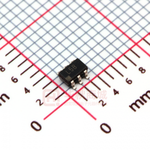
7. 封装信息: - ADP3330采用SOT-23-6封装,具有专利的Chip-on-Lead封装设计,确保在SOT-23封装中具有最佳热性能。与传统SOT-23相比,这种新封装使用电隔离的芯片安装,使所有引脚都有助于热传导,降低了热阻抗。
ADP3330ART-275 价格&库存

很抱歉,暂时无法提供与“ADP3330ART-275”相匹配的价格&库存,您可以联系我们找货

免费人工找货
ADP3330ARTZ3.3-RL7
  •  国内价格
  • 1+13.40325
  • 10+12.7995

库存:40