FEATURES
FUNCTIONAL BLOCK DIAGRAM
Fully regulated adjustable output voltage
High output current: 120 mA
Output accuracy: ±3%
250 kHz switching frequency
Low shutdown current: 2 µA typical
Input voltage range: 3 V to 6 V
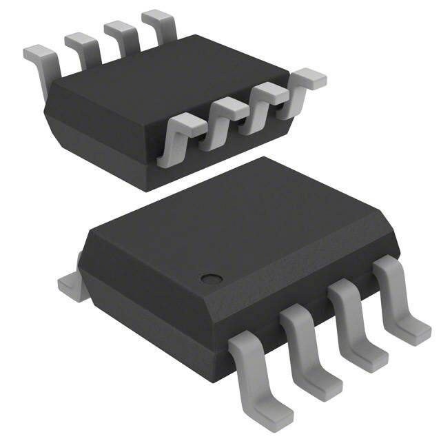
8-Lead SOIC package
−40°C to +85°C ambient temperature range
CP+
CP–
1
3
DNS
SPD
VIN 8
S1
S3
B
ADP3605
SND
DNS
S2
OSC
CLOCK
GEN
SD 4
FEEDBACK
CONTROL
LOOP
APPLICATIONS
Voltage inverters
Voltage regulators
Computer peripherals and add-on cards
Portable instruments
Battery powered devices
Pagers and radio control receivers
Disk drives
Mobile phones
7
VOUT
5
VSENSE
S4
11135-001
Data Sheet
120 mA Switched Capacitor
Voltage Inverter with Regulated Output
ADP3605
2
GND
Figure 1.
GENERAL DESCRIPTION
Pin-for-pin and functionally compatible with the ADP3604, the
internal oscillator of the ADP3605 runs at a 500 kHz nominal
frequency that produces an output switching frequency of
250 kHz. This allows for the use of smaller charge pump and
filter capacitors.
The ADP3605 provides an accuracy of ±3% with a typical
shutdown current of 2 µA. It can also operate from a single
positive input voltage as low as 3 V. The ADP3605 is adjustable
via external resistors over a −3 V to −6 V range.
Rev. B
VIN
8 VIN
*CIN +
4.7µF
VOUT 7
1 CP+
*CP +
4.7µF
+
ADP3605
R1
19kΩ
3 CP–
4 SD
OFF
ON
0
–3.0V
*CO
4.7µF
VSENSE 5
GND
2
*FOR BEST PERFORMANCE, 10µF IS RECOMMENDED
CP: SPRAGUE, 293D475X0010B2W
CIN, CO: TOKIN, 1E475ZY5UC205F
11135-002
The ADP3605 is a 120 mA regulated output, switched capacitor
voltage inverter. It provides a regulated output voltage with
minimum voltage loss and requires a minimum number of
external components. In addition, the ADP3605 does not
require the use of an inductor.
Figure 2. Typical Application Circuit
Document Feedback
Information furnished by Analog Devices is believed to be accurate and reliable. However, no
responsibility is assumed by Analog Devices for its use, nor for any infringements of patents or other
rights of third parties that may result from its use. Specifications subject to change without notice. No
license is granted by implication or otherwise under any patent or patent rights of Analog Devices.
Trademarks and registered trademarks are the property of their respective owners.
One Technology Way, P.O. Box 9106, Norwood, MA 02062-9106, U.S.A.
Tel: 781.329.4700 ©1998–2012 Analog Devices, Inc. All rights reserved.
Technical Support
www.analog.com
�ADP3605
Data Sheet
TABLE OF CONTENTS
Features .............................................................................................. 1
Capacitor Selection .......................................................................9
Applications ....................................................................................... 1
Input Capacitor..............................................................................9
Functional Block Diagram .............................................................. 1
Output Capacitor ..........................................................................9
General Description ......................................................................... 1
Pump Capacitor.......................................................................... 10
Revision History ............................................................................... 2
Shutdown Mode ......................................................................... 10
Specifications..................................................................................... 3
Power Dissipation ...................................................................... 10
Absolute Maximum Ratings ............................................................ 4
General Board Layout Guidelines............................................ 10
ESD Caution.................................................................................. 4
ADP3605 Regulated Adjustable Output Voltage ................... 10
Pin Configuration and Function Descriptions ............................. 5
Regulated Dual Supply System ................................................. 11
Typical Performance Characteristics ............................................. 6
Outline Dimensions ....................................................................... 12
Theory of Operation ........................................................................ 8
Ordering Guide .......................................................................... 12
Applications Information ................................................................ 9
REVISION HISTORY
12/12—Rev. A to Rev. B
Updated Format .................................................................. Universal
Deleted 14-Lead TSSOP .................................................... Universal
Changes to Features Section, General Description Section, and
Figure 2 .............................................................................................. 1
Changes to Table Summary Text Prior to Table 1 and Table 1 ... 3
Changes to Table 2 ............................................................................ 4
Deleted Other Members of ADP36xx Family Table I;
Renumbered Sequentially................................................................ 4
Deleted Figure 4; Renumbered Sequentially................................. 4
Deleted Improved Load Regulation Section ................................. 6
Deleted Maximum Output Voltage Section and Figure 15 ......... 7
Changes to Figure 10 Caption......................................................... 7
Changes to Power Dissipation Section, Regulated Adjustable
Output Voltage Section, and Figure 17 ........................................ 10
Updated Outline Dimensions ....................................................... 12
Changes to Ordering Guide .......................................................... 12
7/99—Rev. 0 to Rev. A
Rev. B | Page 2 of 12
�Data Sheet
ADP3605
SPECIFICATIONS
VIN = 5.0 V at TA = 25°C, CP = CO = 4.7 µF, unless otherwise noted. The CIN, CO, and CP capacitors in the typical application circuit (see Figure 2)
are 4.7 µF. See Figure 2 conditions. All limits at temperature extremes are guaranteed via correlation using standard Statistical Quality
Control (SQC) methods.
Table 1.
Parameter
OPERATING SUPPLY RANGE
SUPPLY CURRENT
Shutdown Mode
OUTPUT RESISTANCE
Open Loop
OUTPUT RIPPLE VOLTAGE
Symbol
VS
IS
SWITCHING FREQUENCY
SHUTDOWN
Logic Input High
Input Current
Logic Input Low
Input Current
fS
RO
VRIPPLE
Test Conditions/Comments
Min
3
Typ
−40°C < TA < +85°C
VSD = VIN, −40°C < TA < +85°C
3
2
CIN = CO = 4.7 µF, ILOAD = 60 mA
ILOAD = 120 mA
VIN = 5 V, −40°C < TA < +85°C
9
38
75
250
VIH
IIH
VIL
IIL
212
Max
6
6
15
Unit
V
mA
µA
288
Ω
mV
mV
kHz
2.4
1
0.4
1
Rev. B | Page 3 of 12
V
µA
V
µA
�ADP3605
Data Sheet
ABSOLUTE MAXIMUM RATINGS
TA = 25°C, unless otherwise noted.
Table 2.
Parameter
Input Voltage (VIN to GND, GND to VOUT)
Input Voltage (VIN to VOUT)
Output Short-Circuit Protection
Power Dissipation, 8-Lead SOIC
θJA 1
Operating Temperature Range
Storage Temperature Range
Lead Temperature (Soldering, 10 sec)
Vapor Phase (60 sec)
Infrared (15 sec)
1
Rating
7.5 V
11 V
1 sec
660 mW
150°C/W
–40°C to +85°C
–65°C to +150°C
300°C
215°C
220°C
Stresses above those listed under Absolute Maximum Ratings
may cause permanent damage to the device. This is a stress
rating only; functional operation of the device at these or any
other conditions above those indicated in the operational
section of this specification is not implied. Exposure to absolute
maximum rating conditions for extended periods may affect
device reliability.
ESD CAUTION
θJA is specified for the worst-case conditions with the device soldered on a
circuit board.
Table 3. Alternative Capacitor Technologies
Type
Aluminum Electrolytic Capacitor
Multilayer Ceramic Capacitor
Solid Tantalum Capacitor
OS-CON Capacitor
1
Life
Fair
Long
Above average
Above average
High Frequency
Fair
Good
Average
Good
Temperature
Fair
Poor
Average
Good
Refer to capacitor manufacturer's data sheet for operation below 0°C.
Table 4. Recommended Capacitor Manufacturers
Manufacturer
Sprague
Sprague
Nichicon
Mallory
TOKIN
Murata
Capacitor
672D, 673D, 674D, 678D
675D, 173D, 199D
PF and PL
TDC and TDL
MLCC
GRM
Capacitor Type
Aluminum electrolytic
Tantalum
Aluminum electrolytic
Tantalum
Multilayer ceramic
Multilayer ceramic
Rev. B | Page 4 of 12
Size
Small
Fair 1
Average
Good
Cost
Low
High
Average
Average
�Data Sheet
ADP3605
CP+
1
GND
2
CP–
3
SD
ADP3605
TOP VIEW
4 (Not to Scale)
8
VIN
7
VOUT
6
NC
5
VSENSE
NOTES
1. NC = NO CONNECT. DO NOT
CONNECT TO THIS PIN.
11135-003
PIN CONFIGURATION AND FUNCTION DESCRIPTIONS
Figure 3. Pin Configuration
Table 5. Pin Function Descriptions
Pin No.
1
2
3
4
Mnemonic
CP+
GND
CP−
SD
5
6
7
VSENSE
NC
VOUT
8
VIN
Description
Positive Terminal for the Pump Capacitor.
Device Ground.
Negative Terminal for the Pump Capacitor.
Logic Level Shutdown Pin. Apply logic high or connect to VIN to shut down the device. In shutdown mode, the
charge pump is turned off, and the quiescent current is reduced to 2 µA (typical). Apply a logic low or connect to
ground for normal operation.
Output Voltage Sense Line. Connect a resistor between this pin and VOUT to set the desired output voltage.
No Connect. Do not connect to this pin.
Regulated Negative Output Voltage. Connect a low ESR, 4.7 µF or larger, capacitor between this pin and the
device ground.
Positive Supply Input Voltage. Connect a low ESR bypass capacitor between this pin and the device ground to
minimize supply transients.
Rev. B | Page 5 of 12
�ADP3605
Data Sheet
TYPICAL PERFORMANCE CHARACTERISTICS
140
270
INPUT CURRENT (mA)
260
100
80
60
40
250
3.0
3.5
4.0
4.5
5.0
SUPPLY VOLTAGE (V)
5.5
0
10
6.0
11135-007
20
11135-004
OSCILLATOR FREQUENCY (kHz)
120
30
50
70
90
LOAD CURRENT (mA)
110
130
Figure 7. Average Input Current vs. Output Current
Figure 4. Oscillator Frequency vs. Supply Voltage
4.5
–2.5
3.0
VIN = 5V
–2.6
2.5
3.0
1.5
NORMAL MODE
(VSD = 0V)
1.0
0.5
0
–15
10
35
TEMPERATURE (°C)
60
–3.0
–3.1
11135-005
1.5
–40
–2.9
–3.2
0
85
80
120
160
200
LOAD CURRENT (mA)
240
280
Figure 8. Output Voltage vs. Load Current, VOUT = −3.0 V
Figure 5. Supply Current vs. Temperature
3.5
300
7
3.0
SUPPLY CURRENT (mA)
IN NORMAL MODE
260
240
2.5
5
2.0
4
1.5
3
1.0
2
220
10
35
TEMPERATURE (°C)
60
SHUTDOWN MODE
(VSD = VIN)
0.5
11135-006
–15
6
NORMAL MODE
(VSD = 0V)
280
200
–40
40
1
0
0
3
85
4
5
SUPPLY VOLTAGE (V)
Figure 9. Supply Current vs. Supply Voltage
Figure 6. Oscillator Frequency vs. Temperature
Rev. B | Page 6 of 12
6
11135-009
2.0
–2.8
SUPPLY CURRENT (µA)
IN SHUTDOWN MODE
2.5
VIN = 3V
VIN = 3.5V
VIN = 4.75V
VIN = 5V
VIN = 6V
–2.7
11135-008
2.0
OUTPUT VOLTAGE (V)
3.5
SUPPLY CURRENT (µA)
IN SHUTDOWN MODE
SHUTDOWN MODE
(VSD = VIN)
OSCILLATOR FREQUENCY (kHz)
SUPPLY CURRENT (mA)
IN NORMAL MODE
4.0
�A1
–0.70V
2ms
11135-011
ADP3605
11135-010
Data Sheet
A2
1V
Figure 10. Start-Up Under Full Load
3.9V
2ms
1V
Figure 11. Enable/Disable Time Under Full Load
Rev. B | Page 7 of 12
�ADP3605
Data Sheet
THEORY OF OPERATION
S1
VIN
S1
S2
+
S2
S3
+
S3
CP
CP
S4
VOUT
CO
S4
VOUT
CO
Figure 13. ADP3605 Switch Configuration Charging the Output Capacitor
11135-012
VIN
During phase one, S1 and S2 are on, charging the pump capacitor
to the input voltage. Before the next phase begins, S1 and S2 are
turned off as well as S3 and S4 to prevent any overlap. S3 and S4
are turned on during the second phase (see Figure 13), and the
charge stored in the pump capacitor is transferred to the output
capacitor.
11135-013
The ADP3605 uses a switched capacitor principle to generate a
negative voltage from a positive input voltage. An onboard
oscillator generates a 2-phase clock to control a switching
network that transfers charge between the storage capacitors. The
switches turn on and off at a 250 kHz rate, which is generated
from an internal 500 kHz oscillator. The basic principle behind
the voltage inversion scheme is illustrated in Figure 12 and
Figure 13.
Figure 12. ADP3605 Switch Configuration Charging the Pump Capacitor
During the second phase, the positive terminal of the pump
capacitor is connected to ground through the variable resistance
switch (S3), and the negative terminal is connected to the output,
resulting in a voltage inversion at the output terminal. Figure 1
shows the ADP3605 block diagram.
Rev. B | Page 8 of 12
�Data Sheet
ADP3605
APPLICATIONS INFORMATION
CAPACITOR SELECTION
INPUT CAPACITOR
The high internal oscillator frequency of the ADP3605 permits
the use of small capacitors for both the pump and the output
capacitors. For a given load current, factors affecting the output
voltage performance are the following:
A small 1 µF input bypass capacitor, preferably with low ESR,
such as tantalum or multilayer ceramic, is recommended to
reduce noise and supply transients and to supply part of the
peak input current drawn by the ADP3605. A large capacitor is
recommended if the input supply is connected to the ADP3605
through long leads, or if the pulse current drawn by the device
may affect other circuitry through supply coupling.
Pump (CP) and output (CO) capacitance
ESR of the CP and CO
When selecting the capacitors, keep in mind that not all
manufacturers guarantee capacitor ESR in the range required
by the circuit. In general, the ESR of the capacitor is inversely
proportional to its physical size; therefore, larger capacitance
values and higher voltage ratings tend to reduce ESR. Because
the ESR is also a function of the operating frequency, when
selecting a capacitor, ensure that its value is rated at the
operating frequency of the circuit.
Temperature is another factor affecting capacitor performance.
Figure 14 illustrates the temperature effect on various capacitors. If
the circuit has to operate at temperatures significantly different
from 25°C, the capacitance and the ESR values must be carefully
selected to adequately compensate for the change. Various
capacitor technologies offer improved performance over
temperature; for example, certain tantalum capacitors provide
good low temperature ESR; however, at a higher cost. Table 3
provides the ratings for different types of capacitor technologies
to help the designer select the right capacitors for the application.
The exact values of CIN and CO are not critical. However, low
ESR capacitors, such as solid tantalum and multilayer ceramic
capacitors, are recommended to minimize voltage loss at high
currents. Table 4 shows a partial list of the recommended low
ESR capacitor manufacturers.
OUTPUT CAPACITOR
The output capacitor (CO) is alternately charged to the CP voltage
when CP is switched in parallel with CO. The ESR of CO introduces
steps in the VOUT waveform whenever the charge pump charges
CO, which contributes to VOUT ripple. Thus, ceramic or tantalum
capacitors are recommended for CO to minimize ripple on the
output. Figure 15 illustrates the output ripple voltage effect for
various capacitance and ESR values. Note that as the capacitor
value increases beyond the point where the dominant contribution
to the output ripple is due to the ESR, no significant reduction
in VOUT ripple is achieved by added capacitance. Because output
current is supplied solely by the output capacitor, CO, during
one-half of the charge pump cycle, peak-to-peak output ripple
voltage is calculated by
V RIPPLE =
IL
+ 2 × I L × ES RCO
2 × f S × CO
where:
IL = load current
fS = 250 kHz nominal switching frequency
CO = 10 µF with an ESR of 0.15 Ω
VRIPPLE =
10
120 mA
2 × 250 kHz × 10 μ F
+ 2 × 120 mA × 0.15 = 60 mV
Multiple smaller capacitors can be connected in parallel to yield
lower ESR and lower cost. For lighter loads, proportionally smaller
capacitors are required. To reduce high frequency noise, bypass
the output with a 0.1 µF ceramic capacitor in parallel with the
output capacitor.
ALUMINUM
1
ESR (Ω)
CERAMIC
100
ADP3605
–3.0V OUTPUT
TANTALUM
0.1
ORGANIC SEMIC
OUTPUT RIPPLE (mV)
11135-014
0.01
–50
80
0
50
TEMPERATURE (°C)
100
Figure 14. ESR vs. Temperature
60
150mΩ
40
100mΩ
20
50mΩ
11135-015
•
•
0
0
20
40
60
80
100
CAPACITANCE (µF)
120
140
Figure 15. Output Ripple Voltage vs. Capacitance and ESR
Rev. B | Page 9 of 12
160
�ADP3605
Data Sheet
PUMP CAPACITOR
The ADP3605 alternately charges CP to the input voltage when
CP is switched in parallel with the input supply, and then transfers
charge to CO when CP is switched in parallel with CO.
During the time CP is charging, the peak current is approximately
two times the output current. During the time CP is delivering
charge to CO, the supply current drops down to about 3 mA.
A low ESR capacitor has a much greater impact on performance
for CP than CO because current through CP is twice the CO current.
Therefore, the voltage drop due to CP is about four times the
ESR of CP times the load current. While the ESR of CO affects
the output ripple voltage, the voltage drop generated by the
ESR of CP, combined with the voltage drop due to the output
source resistance, determines the maximum available VOUT.
SHUTDOWN MODE
ADP3605 REGULATED ADJUSTABLE OUTPUT
VOLTAGE
The regulated output voltage is programmed by a resistor that is
inserted between the VSENSE and VOUT pins, as illustrated in
Figure 16. The inherent limit of the output voltage of a single
inverting charge pump stage is −1 times the input voltage.
The inverse (that is, negative) scaling factor of 1.00 is reduced
somewhat due to losses that increase with output current. To
increase the scaling factor to attain a more negative output voltage,
an external pump stage can be added with passive components,
as is shown in Figure 17. This single stage increases the inverse
scaling factor to a limit of two, although the diode drops limits
the ability to attain that exact 2.00 scaling factor noticeably. Even
further increases can be achieved with additional external
pump stages.
–5
The output of the ADP3605 can be disabled by pulling the SD
pin (Pin 4) high to a TTL/CMOS logic compatible level that
stops the internal oscillator. In shutdown mode, the quiescent
current is reduced to 2 µA (typical). Applying a digital low level or
tying the SD pin to ground turns on the output. If the shutdown
feature is not used, Pin 4 must be tied to the ground pin.
VOUT (V)
R = 29kΩ
POWER DISSIPATION
–4
R = 24kΩ
VIN = 5.0V
8
The power dissipation of the ADP3605 circuit must be limited
such that the junction temperature of the device does not exceed
the maximum junction temperature rating. Total power dissipation
is calculated as
7
ADP3605
R
1
5
4
11135-016
3
2
–3
0
P = (VIN − |VOUT|) IOUT + (VIN) IS
20
40
60
80
LOAD CURRENT (mA)
ADP3605
VIN = 5V
CIN
4.7µF
8 VIN
+
CP +
4.7µF
P ≈ (6 V − |−2.9 V|) 0.12 + (6 V) 0.005 A = 402 mW
VOUT 7
VSENSE 5
•
•
CO
+ 4.7µF
3 CP–
SD
GND
4
2
D1
1N5817
+
C1
4.7µF
GENERAL BOARD LAYOUT GUIDELINES
Use adequate ground and power traces or planes
Use single point ground for device ground and input and
output capacitor grounds
Keep external components as close to the device as possible
Use short traces from the input and output capacitors to
the input and output pins, respectively
R1
44.2kΩ
1 CP+
This is far below the 660 mW power dissipation capability of
the ADP3605.
•
•
120
Figure 16. Adjustable Regulated Output Voltage
For example, assuming worst-case conditions, VIN = 6 V, VOUT =
−2.9 V, IOUT = 120 mA, and IS = 5 mA. Calculated device power
dissipation is
Because the internal switches of the ADP3605 turn on and off
very fast, good printed circuit board (PCB) layout practices are
critical to ensure optimal operation of the device. Improper layouts
results in poor load regulation, especially under heavy loads.
Output performance can be improved by following these
simple layout guidelines:
100
D2
1N5817
+
10µF
11135-017
where:
IOUT and IS are output current and supply current, respectively.
VIN and VOUT are input and output voltages, respectively.
VOUT
Figure 17. Regulated −7 V from a 5 V Input
High accuracy on the adjustable output voltage is achieved with
the use of precision trimmed internal resistors, which eliminate the
need to trim the external resistor or add a second resistor to form a
divider. The adjustable output voltage is set by
VOUT =
1.5
R
9.5 kΩ
where VOUT is in volts and R is in kΩ.
Rev. B | Page 10 of 12
�Data Sheet
ADP3605
REGULATED DUAL SUPPLY SYSTEM
The circuit in Figure 18 provides regulated positive and negative
voltages for systems that require dual supplies from a single
battery or power supply.
1N5817
ADP3607-5
2
VIN
+5V
VOUT 8
CO1
10µF
10µF
CP1 +
10µF
1
CP+
3
CP–
VSENSE 5
SD
GND
4
2
ADP3605
8
CP2 +
10µF
VIN
VOUT 7
1
CP+
3
C P–
–2.6V
R1
16.5kΩ
1%
CO2
+ 10µF
VSENSE 5
SD
GND
4
2
11135-018
VIN = +3.3V
Figure 18. Dual Supply System
Rev. B | Page 11 of 12
�ADP3605
Data Sheet
OUTLINE DIMENSIONS
5.00 (0.1968)
4.80 (0.1890)
1
5
6.20 (0.2441)
5.80 (0.2284)
4
1.27 (0.0500)
BSC
0.25 (0.0098)
0.10 (0.0040)
COPLANARITY
0.10
SEATING
PLANE
1.75 (0.0688)
1.35 (0.0532)
0.51 (0.0201)
0.31 (0.0122)
0.50 (0.0196)
0.25 (0.0099)
45°
8°
0°
0.25 (0.0098)
0.17 (0.0067)
1.27 (0.0500)
0.40 (0.0157)
COMPLIANT TO JEDEC STANDARDS MS-012-AA
CONTROLLING DIMENSIONS ARE IN MILLIMETERS; INCH DIMENSIONS
(IN PARENTHESES) ARE ROUNDED-OFF MILLIMETER EQUIVALENTS FOR
REFERENCE ONLY AND ARE NOT APPROPRIATE FOR USE IN DESIGN.
012407-A
8
4.00 (0.1574)
3.80 (0.1497)
Figure 19. 8-LeadStandard Small Outline Package [SOIC_N]
(R-8)
Dimensions shown in millimeters and (inches)
ORDERING GUIDE
Model 1
ADP3605ARZ
ADP3605ARZ-R7
1
Output
Voltage
Adjustable
Adjustable
Temperature Range
−40°C to +85°C
−40°C to +85°C
Package Description
8-Lead Standard Small Outline Package [SOIC_N], Tube
8-Lead Standard Small Outline Package [SOIC_N], 7” Tape and Reel
Z = RoHS Compliant Part.
©1998–2012 Analog Devices, Inc. All rights reserved. Trademarks and
registered trademarks are the property of their respective owners.
D11135-0-12/12(B)
Rev. B | Page 12 of 12
Package
Option
R-8
R-8
�