FUNCTIONAL BLOCK DIAGRAM
APPLICATIONS
GND
NIC
NIC
GND
RFIN
GND
NIC
GND
1
2
3
4
5
6
7
8
24
23
22
21
20
19
18
17
GND
NIC
NIC
NIC
VGG1
NIC
ACG3
GND
9
10
11
12
13
14
15
16
Military and space
Test instrumentation
ADPA9002
GND
NIC
GND
RFOUT/VDD
GND
NIC
NIC
GND
PACKAGE
BASE
GND
21196-001
OP1dB: 29 dBm typical
Gain: up to 15 dB typical
OIP3: up to 43 dBm typical
Self biased at VDD = 12 V at 385 mA typical with an optional
bias control on VGG1 for IDQ adjustment
50 Ω matched input/output
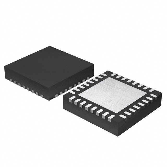
32-lead, 5 mm × 5 mm LFCSP
GND
NIC
ACG1
ACG2
NIC
NIC
NIC
GND
FEATURES
32
31
30
29
28
27
26
25
Data Sheet
GaAs, pHEMT, MMIC, Single Positive Supply,
DC to 10 GHz Power Amplifier
ADPA9002
Figure 1.
GENERAL DESCRIPTION
The ADPA9002 is a gallium arsenide (GaAs), pseudomorphic
high electron mobility transistor (pHEMT), monolithic
microwave integrated circuit (MMIC), power amplifier that
operates between dc and 10 GHz. The amplifier provides 15 dB
of gain, 42 dBm of OIP3, and 31.5 dBm of saturated output
power (PSAT) while requiring 385 mA from a 12 V supply. The
ADPA9002 is self biased in normal operation and has an
optional bias control for supply quiescent current (IDQ)
adjustment. The amplifier is ideal for military and space and
Rev. 0
test equipment applications. The ADPA9002 also features inputs
and outputs that are internally matched to 50 Ω, housed in a
RoHS compliant, 5 mm × 5 mm LFCSP premolded cavity
package, making it compatible with high volume surface-mount
technology (SMT) assembly equipment.
Note that throughout this data sheet, multifunction pins, such
as RFOUT/VDD, are referred to either by the entire pin name or
by a single function of the pin, for example, VDD, when only that
function is relevant.
Document Feedback
Information furnished by Analog Devices is believed to be accurate and reliable. However, no
responsibility is assumed by Analog Devices for its use, nor for any infringements of patents or other
rights of third parties that may result from its use. Specifications subject to change without notice. No
license is granted by implication or otherwise under any patent or patent rights of Analog Devices.
Trademarks and registered trademarks are the property of their respective owners.
One Technology Way, P.O. Box 9106, Norwood, MA 02062-9106, U.S.A.
Tel: 781.329.4700
©2019 Analog Devices, Inc. All rights reserved.
Technical Support
www.analog.com
�ADPA9002
Data Sheet
TABLE OF CONTENTS
Features .............................................................................................. 1
ESD Caution...................................................................................5
Applications ....................................................................................... 1
Pin Configuration and Function Descriptions..............................6
Functional Block Diagram .............................................................. 1
Interface Schematics .....................................................................7
General Description ......................................................................... 1
Typical Performance Characteristics ..............................................8
Revision History ............................................................................... 2
Constant IDD Operation ............................................................. 16
Specifications..................................................................................... 3
Theory of Operation ...................................................................... 17
DC to 2 GHz ................................................................................. 3
Applications Information .............................................................. 18
2 GHz to 5 GHz ............................................................................ 3
Typical Application Circuit ....................................................... 18
5 GHz to 10 GHz .......................................................................... 4
Outline Dimensions ....................................................................... 19
Absolute Maximum Ratings ............................................................ 5
Ordering Guide .......................................................................... 19
Thermal Resistance ...................................................................... 5
REVISION HISTORY
10/2019—Revision 0: Initial Version
Rev. 0 | Page 2 of 19
�Data Sheet
ADPA9002
SPECIFICATIONS
DC TO 2 GHz
TA = 25°C, VDD = 12 V, IDQ = 385 mA, VGG1= GND for nominal self biased operation, and frequency range = dc to 2 GHz, with a 50 Ω
matched input and output, unless otherwise noted.
Table 1.
Parameter
FREQUENCY RANGE
GAIN
Gain Variation Over Temperature
NOISE FIGURE
RETURN LOSS
Input
Output
OUTPUT
Output Power for 1 dB Compression
Saturated Output Power
Output Third-Order Intercept
SUPPLY
Quiescent Current
Drain Voltage
Symbol
OP1dB
PSAT
OIP3
Min
DC
12.5
27
IDQ
VDD
10
Typ
14.5
±0.01
5
Unit
GHz
dB
dB/°C
dB
18
14
dB
dB
29
31
43
dBm
dBm
dBm
385
mA
12
Max
2
15
Test Conditions/Comments
Measurement taken at output power (POUT) per tone =
14 dBm
For external bias control, adjust VGG1 between −2 V and
+0.5 V to achieve the desired IDQ
V
2 GHz TO 5 GHz
TA = 25°C, VDD = 12 V, IDQ = 385 mA, VGG1 = GND for nominal self biased operation, and frequency range = 2 GHz to 5 GHz, unless
otherwise noted. 50 Ω matched input/output.
Table 2.
Parameter
FREQUENCY RANGE
GAIN
Gain Variation Over Temperature
NOISE FIGURE
RETURN LOSS
Input
Output
OUTPUT
Output Power for 1 dB Compression
Saturated Output Power
Output Third-Order Intercept
SUPPLY
Quiescent Current
Drain Voltage
Symbol
OP1dB
PSAT
OIP3
Min
2
13
27
IDQ
VDD
10
Typ
15
±0.008
3
Unit
GHz
dB
dB/°C
dB
14
15
dB
dB
29
31.5
42
dBm
dBm
dBm
385
mA
12
Max
5
15
V
Rev. 0 | Page 3 of 19
Test Conditions/Comments
Measurement taken at POUT per tone = 14 dBm
For external bias control, adjust VGG1 between −2 V and
+0.5 V to achieve the desired IDQ
�ADPA9002
Data Sheet
5 GHz TO 10 GHz
TA = 25°C, VDD = 12 V, IDQ = 385 mA, VGG1 = GND for nominal self biased operation, and frequency range = 5 GHz to 10 GHz, with a
50 Ω matched input and output, unless otherwise noted.
Table 3.
Parameter
FREQUENCY RANGE
GAIN
Gain Variation Over Temperature
NOISE FIGURE
RETURN LOSS
Input
Output
OUTPUT
Output Power for 1 dB Compression
Saturated Output Power
Output Third-Order Intercept
SUPPLY
Quiescent Current
Drain Voltage
Symbol
OP1dB
PSAT
OIP3
Min
5
13.5
25
IDQ
VDD
10
Typ
15.5
±0.016
4
Unit
GHz
dB
dB/°C
dB
19
13
dB
dB
28
31
40.5
dBm
dBm
dBm
385
mA
12
Max
10
15
Rev. 0 | Page 4 of 19
V
Test Conditions/Comments
Measurement taken at POUT/tone = 14 dBm
For external bias control, adjust VGG1 between
−2 V and +0.5 V to achieve the desired IDQ
�Data Sheet
ADPA9002
ABSOLUTE MAXIMUM RATINGS
THERMAL RESISTANCE
Table 4.
Parameter
VDD
VGG1
RFIN
Continuous Power Dissipation (PDISS), T = 85°C
(Derate 113.64 mW/°C Above 85°C)
Output Load Voltage Standing Wave Ratio
(VSWR)
Temperature
Storage Range
Operating Range
Peak Reflow (Moisture Sensitivity Level
(MSL) 3)
Junction to Maintain 1 Million Hour Mean
Time to Failure (MTTF)
Nominal Junction (T = 85°C, VDD = 12 V)
Rating
16 V
−2.5 V to +1 V
25 dBm
10.2 W
Thermal performance is directly linked to printed circuit board
(PCB) design and operating environment. Careful attention to
PCB thermal design is required. θJC is the junction to case
thermal resistance.
7:1
Package
CG-32-2
−65°C to +150°C
−40°C to +85°C
260°C
ESD CAUTION
Table 5. Thermal Resistance
175°C
125.7°C
ESD Sensitivity
Human Body Model (HBM)
Class 1B, passed
500 V
Stresses at or above those listed under Absolute Maximum
Ratings may cause permanent damage to the product. This is a
stress rating only; functional operation of the product at these
or any other conditions above those indicated in the operational
section of this specification is not implied. Operation beyond
the maximum operating conditions for extended periods may
affect product reliability.
Rev. 0 | Page 5 of 19
θJC
8.8
Unit
°C/W
�ADPA9002
Data Sheet
32
31
30
29
28
27
26
25
GND
NIC
ACG1
ACG2
NIC
NIC
NIC
GND
PIN CONFIGURATION AND FUNCTION DESCRIPTIONS
ADPA9002
TOP VIEW
(Not to Scale)
GND
NIC
NIC
NIC
VGG1
NIC
ACG3
GND
24
23
22
21
20
19
18
17
GND
NIC
GND
RFOUT/VDD
GND
NIC
NIC
GND
PACKAGE
BASE
GND
NOTES
1. NIC = NOT INTERNALLY CONNECTED. THESE PINS
MUST BE CONNECTED TO RF AND DC GROUND.
2. EXPOSED PAD. THE EXPOSED PAD MUST BE
CONNECTED TO RF AND DC GROUND.
21196-002
1
2
3
4
5
6
7
8
9
10
11
12
13
14
15
16
GND
NIC
NIC
GND
RFIN
GND
NIC
GND
Figure 2. Pin Configuration
Table 6. Pin Function Descriptions
Pin No.
1, 4, 6, 8, 9, 16, 17, 20,
22, 24, 25, 32
2, 3, 7, 10, 11, 12, 14, 18,
19, 23, 26, 27, 28, 31
5
13
Mnemonic
GND
Description
Ground. These pins must be connected to RF and dc ground.
NIC
Not Internally Connected. These pins must be connected to RF and dc ground.
RFIN
VGG1
15, 29, 30
ACG3, ACG2, ACG1
21
RFOUT/VDD
RF Input. This pin is dc-coupled and matched to 50 Ω. See Figure 6 for the interface schematic.
Gate Voltage. This pin is used for external bias operation of the device. If grounded, the amplifier
runs in self biased mode at the standard current of 385 mA. Adjusting the voltage above or
below the ground potential controls the drain current. External bypass capacitors are required
(see Figure 62). See Figure 7 for the interface schematic.
AC Ground Pins. These pins are used for low frequency termination. External bypass
capacitor required (see Figure 62). See Figure 4 and Figure 5 for the interface schematics.
RF Output for the Amplifier (RFOUT).
Drain Voltage (VDD). Connect the VDD network to provide the drain current (IDD) (see Figure 62).
See Figure 5 for the interface schematic.
Exposed Pad. The exposed pad must be connected to RF and dc ground.
EPAD
Rev. 0 | Page 6 of 19
�Data Sheet
ADPA9002
Figure 3. GND Interface Schematic
Figure 6. RFIN Interface Schematic
ACG3
21196-004
RFIN
VGG1
Figure 7. VGG1 Interface Schematic
RFOUT/VDD
21196-005
Figure 4. ACG3 Interface Schematic
ACG1
ACG2
21196-006
RFIN
21196-007
GND
21196-003
INTERFACE SCHEMATICS
Figure 5. RFOUT/VDD, ACG1, ACG2 Interface Schematic
Rev. 0 | Page 7 of 19
�ADPA9002
Data Sheet
20
15
15
10
10
5
S22 (dB)
S21 (dB)
S11 (dB)
0
–5
–5
–10
–15
–15
0
100
200
300
400
500
FREQUENCY (MHz)
S22 (dB)
S21 (dB)
S11 (dB)
0
–10
–20
–20
0
2
4
6
8
10
12
14
16
FREQUENCY (GHz)
Figure 8. S22, S21, and S11 vs. Frequency, 10 MHz to 500 MHz,
Self Biased Mode, VDD = 12 V, VGG1 = GND
Figure 11. S22, S21, and S11 vs. Frequency, 500 MHz to 16 GHz,
Self Biased Mode, VDD = 12 V, VGG1 = GND
18
18
16
16
14
14
GAIN (dB)
12
10
12
10
8
8
TA = +85°C
TA = +25°C
TA = –40°C
0
2
4
6
8
10
12
FREQUENCY (GHz)
6
21196-009
6
Figure 9. Gain vs. Frequency for Various Temperatures, Self Biased Mode,
VDD = 12 V, VGG1 = GND
15V, 410mA
12V, 385mA
10V, 375mA
0
2
4
6
8
10
12
FREQUENCY (GHz)
21196-012
GAIN (dB)
5
21196-011
S22, S21, AND S11 (dB)
20
21196-008
S22, S21, AND S11 (dB)
TYPICAL PERFORMANCE CHARACTERISTICS
Figure 12. Gain vs. Frequency for Various VDD and Quiescent Currents,
Self Biased Mode, VGG1 = GND
18
0
TA = +85°C
TA = +25°C
TA = –40°C
16
INPUT RETURN LOSS (dB)
–4
12
10
500mA
400mA
300mA
385mA, SELF BIASED
6
0
2
4
6
FREQUENCY (GHz)
8
10
–12
–16
12
21196-010
8
–8
Figure 10. Gain vs. Frequency for Various IDQ, Externally Biased Mode,
VDD = 12 V, Controlled VGG1
–20
0
2
4
6
8
10
12
FREQUENCY (GHz)
Figure 13. Input Return Loss vs. Frequency for Various Temperatures,
Self Biased Mode, VDD = 12 V, VGG1 = GND
Rev. 0 | Page 8 of 19
21196-013
GAIN (dB)
14
�Data Sheet
ADPA9002
0
0
15V, 410mA
12V, 385mA
10V, 375mA
–4
INPUT RETURN LOSS (dB)
–8
–12
–16
4
6
8
10
12
FREQUENCY (GHz)
–20
Figure 14. Input Return Loss vs. Frequency for Various VDD and Quiescent
Currents, Self Biased Mode, VGG1 = GND
0
2
4
6
8
10
21196-017
2
21196-014
0
12
FREQUENCY (GHz)
Figure 17. Input Return Loss vs. Frequency for Various IDQ, Externally Biased
Mode, VDD = 12 V, Controlled VGG1
0
0
15V, 410mA
12V, 385mA
10V, 375mA
TA = +85°C
TA = +25°C
TA = –40°C
OUTPUT RETURN LOSS (dB)
–4
–8
–12
–16
–20
0
2
4
6
8
10
12
FREQUENCY (GHz)
Figure 15. Output Return Loss vs. Frequency for Various Temperatures,
Self Biased Mode, VDD = 12 V, VGG1 = GND
–4
–8
–12
–16
–20
21196-015
OUTPUT RETURN LOSS (dB)
–12
–16
–20
0
2
4
6
8
10
12
FREQUENCY (GHz)
Figure 18. Output Return Loss vs. Frequency for Various VDD and Quiescent
Currents, Self Biased Mode, VGG1 = GND
0
0
500mA
400mA
300mA
385mA, SELF BIASED
–4
TA = +85°C
TA = +25°C
TA = –40°C
–10
REVERSE ISOLATION (dB)
OUTPUT RETURN LOSS (dB)
–8
21196-018
INPUT RETURN LOSS (dB)
–4
500mA
400mA
300mA
385mA, SELF BIASED
–8
–12
–20
–30
–40
–50
–60
–16
0
2
4
6
FREQUENCY (GHz)
8
10
12
Figure 16. Output Return Loss vs. Frequency for Various IDQ, External Biased
Condition, VDD = 12 V, Controlled VGG1
Rev. 0 | Page 9 of 19
–80
0
2
4
6
FREQUENCY (GHz)
8
10
12
21196-019
–20
21196-016
–70
Figure 19. Reverse Isolation vs. Frequency for Various Temperatures,
Self Biased Mode, VDD = 12 V, VGG1 = GND
�ADPA9002
Data Sheet
16
16
TA = +85°C
TA = +25°C
TA = –40°C
14
10
8
6
8
6
4
4
2
2
0
10
40
30
20
60
50
70
80
90
100
FREQUENCY (MHz)
Figure 20. Noise Figure vs. Frequency, 10 MHz to 100 MHz, for Various
Temperatures, Self Biased Mode, VDD = 12 V, VGG1 = GND
0
4
6
8
10
12
FREQUENCY (GHz)
Figure 23. Noise Figure vs. Frequency, 100 MHz to 12 GHz, for Various
Temperatures, Self Biased Mode, VDD = 12 V, VGG1 = GND
32
32
30
30
28
28
26
2
0
OP1dB (dBm)
26
24
22
22
TA = +85°C
TA = +25°C
TA = –40°C
0
0.1
0.2
0.3
0.4
0.5
0.6
0.7
0.8
0.9
1.0
FREQUENCY (GHz)
20
21196-021
20
Figure 21. OP1dB vs. Frequency,10 MHz to 1 GHz for Various Temperatures,
Self Biased Mode, VDD = 12 V, VGG1 = GND
0
1
2
3
4
5
6
7
8
9
10
11
12
FREQUENCY (GHz)
Figure 24. OP1dB vs. Frequency, 1 GHz to 12 GHz for Various Temperatures,
Self Biased Mode, VDD = 12 V, VGG1 = GND
32
30
30
28
28
OP1dB (dBm)
32
26
TA = +85°C
TA = +25°C
TA = –40°C
21196-024
24
26
24
24
22
1
2
3
4
5
6
7
FREQUENCY (GHz)
8
9
10
11
12
21196-022
20
0
500mA
400mA
300mA
385mA, SELF BIASED
22
15V, 410mA
12V, 385mA
10V, 375mA
Figure 22. OP1dB vs. Frequency for Various VDD and Quiescent Currents, Self
Biased Mode, VGG1 = GND
Rev. 0 | Page 10 of 19
20
0
1
2
3
4
5
6
7
8
9
10
11
FREQUENCY (GHz)
Figure 25. OP1dB vs. Frequency for Various IDQ,
Externally Biased Mode, VDD = 12 V, Controlled VGG1
12
21196-025
OP1dB (dBm)
10
21196-023
NOISE FIGURE (dB)
12
21196-020
NOISE FIGURE (dB)
12
OP1dB (dBm)
TA = +85°C
TA = +25°C
TA = –40°C
14
�ADPA9002
36
36
34
34
32
32
30
30
PSAT (dBm)
28
26
TA = +85°C
TA = +25°C
TA = –40°C
0.1
0.2
0.3
0.4
0.5
0.6
0.7
0.8
0.9
20
21196-026
20
0
TA = +85°C
TA = +25°C
TA = –40°C
22
1.0
FREQUENCY (GHz)
Figure 26. PSAT vs. Low Frequency,10 MHz to 1 GHz for Various Temperatures,
Self Biased Mode, VDD = 12 V, VGG1 = GND
0
3
4
5
6
7
8
9
10
11
12
Figure 29. PSAT vs. Frequency, 1 GHz to 12 GHz for Various Temperatures,
Self Biased Mode, VDD = 12 V, VGG1 = GND
34
34
32
32
30
30
PSAT (dBm)
36
26
2
FREQUENCY (GHz)
36
28
1
21196-029
22
24
28
26
24
15V, 410mA
12V, 385mA
10V, 375mA
20
0
1
2
3
4
5
6
7
8
9
10
11
500mA
400mA
300mA
385mA, SELF BIASED
22
12
FREQUENCY (GHz)
20
21196-027
22
0
2
3
4
5
6
7
8
9
10
11
12
FREQUENCY (GHz)
Figure 27. PSAT vs. Frequency for Various VDD and Quiescent Currents,
Self Biased Mode, VGG1 = GND
Figure 30. PSAT vs. Frequency for Various IDQ, Externally Biased Mode,
VDD = 12 V, Controlled VGG1
30
27
27
24
24
21
21
18
18
PAE (%)
30
15
1
21196-030
PSAT (dBm)
26
24
24
PAE (%)
28
15
12
12
9
9
6
6
TA = +85°C
TA = +25°C
TA = –40°C
0
0
1
2
3
4
5
6
7
FREQUENCY (GHz)
8
9
10
11
15V, 410mA
12V, 385mA
10V, 375mA
3
12
0
21196-028
3
Figure 28. Power Added Efficiency (PAE) vs. Frequency for Various Temperatures,
Self Biased Mode, VDD = 12 V, VGG1 = GND, PAE Measured at PSAT
0
1
2
3
4
5
6
7
FREQUENCY (GHz)
8
9
10
11
12
21196-031
PSAT (dBm)
Data Sheet
Figure 31. PAE vs. Frequency for Various VDD and Quiescent Currents,
Self Biased Mode, VGG1 = GND, PAE Measured at PSAT
Rev. 0 | Page 11 of 19
�ADPA9002
Data Sheet
35
27
30
21
15
12
9
500mA
400mA
300mA
385mA, SELF BIASED
3
2
3
4
5
6
7
8
9
10
11
21196-032
1
440
15
430
420
10
410
5
0
12
FREQUENCY (GHz)
0
–5
470
POUT (dBm), GAIN (dB), PAE (%)
30
460
25
450
20
440
15
430
420
10
410
5
5
10
15
20
35
490
20
470
15
450
10
430
5
410
0
–5
POUT (dBm), GAIN (dB), PAE (%)
30
500
15
440
10
420
400
5
400
380
0
–5
440
15
INPUT POWER (dBm)
20
21196-034
420
10
500
460
15
5
520
PAE
GAIN
POUT
IDD
20
460
0
20
480
20
5
15
25
480
10
10
35
520
25
5
INPUT POWER (dBm)
540
PAE
GAIN
POUT
IDD
390
0
Figure 36. POUT, Gain, PAE, IDD vs. Input Power, 6 GHz,
Self Biased Mode, VDD = 12 V, VGG1 = GND
IDD (mA)
POUT (dBm), GAIN (dB), PAE (%)
510
25
Figure 33. POUT, Gain, PAE, Supply Current (IDD) vs. Input Power, 3 GHz,
Self Biased Mode, VDD = 12 V, VGG1 = GND
0
–5
530
PAE
GAIN
POUT
IDD
Figure 34. POUT, Gain, PAE, IDD vs. Input Power, 8 GHz,
Self Biased Mode, VDD = 12 V, VGG1 = GND
380
0
5
10
15
INPUT POWER (dBm)
Figure 37. POUT, Gain, PAE, IDD vs. Input Power, 10 GHz,
Self Biased Mode, VDD = 12 V, VGG1 = GND
Rev. 0 | Page 12 of 19
20
21196-037
390
0
INPUT POWER (dBm)
30
20
15
400
21196-033
0
–5
10
35
IDD (mA)
POUT (dBm), GAIN (dB), PAE (%)
30
5
Figure 35. POUT, Gain, PAE, IDD vs. Input Power, 1 GHz,
Self Biased Mode, VDD = 12 V, VGG1 = GND
480
PAE
GAIN
POUT
IDD
390
0
INPUT POWER (dBm)
Figure 32. PAE vs. Frequency for Various IDQ, Externally Biased Mode,
VDD = 12 V, Controlled VGG1, PAE Measured at PSAT
35
400
21196-036
0
450
20
IDD (mA)
6
460
25
IDD (mA)
PAE (%)
18
470
IDD (mA)
POUT (dBm), GAIN (dB), PAE (%)
24
480
PAE
GAIN
POUT
IDD
21196-035
30
�ADPA9002
50
5
45
4
40
1GHz
2GHz
3GHz
4GHz
5GHz
6GHz
7GHz
8GHz
9GHz
10GHz
2
1
0
–5
30
25
TA = +85°C
TA = +25°C
TA = –40°C
20
0
5
10
15
20
INPUT POWER (dBm)
0
2
3
4
5
6
7
8
9
10
11
12
Figure 41. OIP3 vs. Frequency for Various Temperatures,
POUT per Tone = 14 dBm, Self Biased Mode, VDD = 12 V, VGG1 = GND
50
45
45
40
40
OIP3 (dBm)
50
35
1
FREQUENCY (GHz)
Figure 38. Power Dissipation vs. Input Power for Various Frequencies at TA =
85°C, Self Biased Mode, VDD = 12 V, VGG1 = GND
35
30
30
25
1
2
3
4
5
6
7
8
9
10
11
12
FREQUENCY (GHz)
20
21196-039
20
0
500mA
400mA
300mA
SELF BIASED
25
15V, 410mA
12V, 385mA
10V, 375mA
Figure 39. OIP3 vs. Frequency for Various VDD and Quiescent Currents,
Self Biased Mode, VGG1 = GND, POUT per Tone = 14 dBm
0
1
2
3
4
5
6
7
8
9
10
11
12
FREQUENCY (GHz)
21196-042
OIP3 (dBm)
35
21196-041
3
OIP3 (dBm)
6
21196-038
POWER DISSIPATION (W)
Data Sheet
Figure 42. OIP3 vs. Frequency for Various IDQ, Externally Biased Mode,
VDD = 12 V, Controlled VGG1, POUT per Tone = 14 dBm
100
50
90
45
80
70
35
30
10
2
3
4
5
6
7
FREQUENCY (GHz)
8
9
10
11
12
0
21196-040
1
1GHz
2GHz
3GHz
4GHz
5GHz
6GHz
7GHz
8GHz
9GHz
10GHz
40
20
20
0
50
30
10dBm
12dBm
14dBm
16dBm
18dBm
20dBm
25
60
Figure 40. OIP3 vs. Frequency for Various POUT per Tone, Self Biased Mode,
VDD = 12 V, VGG1 = GND
0
2
4
6
8
10
12
14
POUT PER TONE (dBm)
16
18
20
21196-043
IM3 (dBc)
OIP3 (dBm)
40
Figure 43. Third-Order Intermodulation Distortion Relative to Carrier (IM3) vs.
POUT per Tone for Various Frequencies, Self Biased Mode, VDD = 10 V,
VGG1 = GND
Rev. 0 | Page 13 of 19
�Data Sheet
90
90
80
80
70
70
60
60
50
1GHz
2GHz
3GHz
4GHz
5GHz
6GHz
7GHz
8GHz
9GHz
10GHz
40
30
20
10
20
10
4
2
8
6
10
12
16
14
18
20
POUT PER TONE (dBm)
0
0
60
55
55
50
50
45
45
35
4
8
6
10
12
16
14
18
20
Figure 47. IM3 vs. POUT per Tone for Various Frequencies, Self Biased Mode,
VDD = 15 V, VGG1 = GND
60
40
2
POUT PER TONE (dBm)
OIP2 (dBm)
40
35
30
TA = +85°C
TA = +25°C
TA = –40°C
20
0
1
2
3
4
5
6
7
8
9
10
11
15V, 410mA
12V, 385mA
10V, 375mA
25
12
FREQUENCY (GHz)
20
21196-045
25
Figure 45. OIP2 vs. Frequency for Various Temperatures,
POUT per Tone = 14 dBm, Self Biased, VDD = 12 V, VGG1 = GND
0
1
55
50
50
45
45
OIP2 (dBm)
55
40
35
30
2
3
4
5
6
7
FREQUENCY (GHz)
8
9
10
11
12
6
7
8
9
10
11
12
35
10dBm
12dBm
14dBm
16dBm
18dBm
20dBm
25
20
21196-046
1
5
40
30
500mA
400mA
300mA
SELF BIASED
0
4
Figure 48. OIP2 vs. Frequency for Various VDD and Quiescent Currents, Self
Biased Mode, VGG1 = GND, POUT per Tone = 14 dBm
60
20
3
FREQUENCY (GHz)
60
25
2
21196-048
30
Figure 46. OIP2 vs. Frequency for Various IDQ, Externally Biased Mode,
VDD = 12 V, Controlled VGG1, POUT per Tone = 14 dBm
0
1
2
3
4
5
6
7
FREQUENCY (GHz)
8
9
10
11
12
21196-049
OIP2 (dBm)
Figure 44. IM3 vs. POUT per Tone for Various Frequencies, Self Biased Mode,
VDD = 12 V, VGG1 = GND
OIP2 (dBm)
1GHz
2GHz
3GHz
4GHz
5GHz
6GHz
7GHz
8GHz
9GHz
10GHz
40
30
0
0
50
21196-047
100
IM3 (dBc)
100
21196-044
IM3 (dBc)
ADPA9002
Figure 49. OIP2 vs. Frequency for Various POUT per Tone, Self Biased Mode,
VDD = 12 V, VGG1 = GND
Rev. 0 | Page 14 of 19
�Data Sheet
ADPA9002
570
570
520
470
520
495
470
445
445
420
420
395
395
370
–5
0
5
10
15
20
INPUT POWER (dBm)
370
–5
21196-050
IDD (mA)
495
10
15
20
500
1GHz
2GHz
3GHz
4GHz
5GHz
6GHz
7GHz
8GHz
9GHz
10GHz
450
IDQ (mA)
IGG1 (mA)
0.2
5
Figure 53. IDD vs. Input Power for Various Frequencies,
VDD = 12 V, IDQ = 400 mA, Controlled VGG1
0.5
0.3
0
INPUT POWER (dBm)
Figure 50. IDD vs. Input Power for Various Frequencies,
Self Biased Mode, VDD = 12 V, VGG1 = GND
0.4
1GHz
2GHz
3GHz
4GHz
5GHz
6GHz
7GHz
8GHz
9GHz
10GHz
545
IDD (mA)
545
21196-053
1GHz
2GHz
3GHz
4GHz
5GHz
6GHz
7GHz
8GHz
9GHz
10GHz
0.1
400
350
0
0
5
10
15
20
INPUT POWER (dBm)
21196-051
–0.2
–5
Figure 51. Gate 1 Current (IGG1) vs. Input Power for Various Frequencies,
VDD = 12 V, IDQ = 400 mA, Controlled VGG1
1000
900
800
600
500
400
300
200
100
0
–2.0
–1.5
–1.0
–0.5
0
0.5
VGG1 (V)
1.0
21196-052
IDQ (mA)
700
Figure 52. IDQ vs. VGG1, VDD = 12 V, Externally Biased Mode
Rev. 0 | Page 15 of 19
250
2
4
6
8
10
12
14
VDD (V)
Figure 54. IDQ vs. VDD, VGG1 = GND, Self Biased Mode
16
21196-054
300
–0.1
�ADPA9002
Data Sheet
CONSTANT IDD OPERATION
32
32
30
30
28
28
OP1dB (dBm)
26
26
24
24
22
22
TA = +85°C
TA = +25°C
TA = –40°C
0
1
2
3
4
5
6
7
8
9
10
FREQUENCY (GHz)
20
21196-055
20
15V
12V
10V
0
1
2
3
4
5
6
7
8
9
10
FREQUENCY (GHz)
Figure 55. OP1dB vs. Frequency for Various Temperatures, VDD = 12 V,
Constant IDD = 400 mA
21196-058
OP1dB (dBm)
Biased with the HMC980LP4E active bias controller for constant IDD operation. TA = 25°C, VDD = 12 V, and IDQ = 400 mA for nominal
operation, unless otherwise noted.
Figure 58. OP1dB vs. Frequency for Various Supply Voltages,
Constant IDD = 400 mA
34
32
32
30
30
PSAT (dBm)
OP1dB (dBm)
28
26
28
26
24
24
500mA
400mA
300mA
1
2
3
4
5
6
7
8
9
10
FREQUENCY (GHz)
Figure 56. OP1dB vs. Frequency for Various Constant IDD, VDD = 12 V
0
1
2
3
4
5
6
7
8
9
10
FREQUENCY (GHz)
Figure 59. PSAT vs. Frequency for Various Temperatures, VDD = 12 V,
Constant IDD = 400 mA
34
32
32
30
30
PSAT (dBm)
34
28
26
28
26
24
15V
12V
10V
22
20
0
1
2
3
4
5
6
7
8
9
FREQUENCY (GHz)
500mA
400mA
300mA
22
10
20
0
1
2
3
4
5
6
7
8
9
10
FREQUENCY (GHz)
Figure 57. PSAT vs. Frequency for Various Supply Voltages,
Constant IDD = 400 mA
Figure 60. PSAT vs. Frequency for Various Constant IDD, VDD = 12 V
Rev. 0 | Page 16 of 19
21196-060
24
21196-057
PSAT (dBm)
20
21196-056
20
0
TA = +85°C
TA = +25°C
TA = –40°C
22
21196-059
22
�Data Sheet
ADPA9002
THEORY OF OPERATION
The ADPA9002 is a GaAs, MMIC, pHEMT, cascode distributed
power amplifier. The cascode distributed architecture of the
ADPA9002 uses a fundamental cell consisting of a stack of two
field effect transistors (FETs) with the source of the upper FET
connected to the drain of the lower FET. The fundamental cell
is then duplicated several times with an RFIN transmission line
interconnecting the gates of the lower FETs and an RFOUT
transmission line interconnecting the drains of the upper FETs.
ACG1 ACG2
VGG1 ACG3
21196-061
RFOUT/
VDD
RFIN
Figure 61. Simplified Schematic of the Cascode Distributed Amplifier
Additional circuit design techniques are used around each cell
to optimize the overall bandwidth, output power, and noise
figure. The major benefit of this architecture is that a high
output level is maintained across a bandwidth far greater than a
single instance of the fundamental cell provides. A simplified
schematic of this architecture is shown in Figure 61.
For simplified biasing without the need for a negative voltage
rail, VGG1 can be connected directly to GND. With VDD = 12 V
and VGG1 grounded, a quiescent drain current of 385 mA (typical)
results. An externally generated VGG1 can optionally be applied,
allowing adjustment of the quiescent drain current above and
below the 385 mA nominal. As an example, Figure 52 shows that,
by adjusting VGG1 from approximately −0.3 V to +0.3 V, quiescent
drain currents from 250 mA to 450 mA can be obtained.
The ADPA9002 has single-ended input and output ports whose
impedances are nominally equal to 50 Ω over the dc to 10 GHz
frequency range. Consequently, the ADPA9002 can be directly
inserted into a 50 Ω system with no required impedance
matching circuitry. Similarly, the input and output impedances
are sufficiently stable across variations in temperature and
supply voltage so that no impedance matching compensation is
required. The RF output port additionally functions as the VDD
bias, requiring an RF choke through which dc bias is applied.
Though the device operates down to dc, blocking capacitors are
recommended at the RF input and output ports to prevent
damages on the RF stages when loading the dc bias supplies. The
RF choke and blocking capacitor at the RF output together
constitute a bias tee. In practice, the external RF choke and dc
blocking capacitor selections limit the lowest frequency of
operation.
ACG1 through ACG3 are nodes at which ac terminations
(capacitors) to ground can be provided. The use of such
terminations serves to roll off the gain at frequencies below
200 MHz, allowing the flattest possible gain response to be
obtained over various frequencies.
It is critical to supply low inductance ground connections to the
GND pins and to the package base exposed pad to ensure stable
operation. To achieve optimal performance from the ADPA9002
and to prevent damage to the device, do not exceed the absolute
maximum ratings.
Rev. 0 | Page 17 of 19
�ADPA9002
Data Sheet
APPLICATIONS INFORMATION
Capacitive bypassing is required for VDD and VGG1, as shown in
Figure 62. Both the RFIN and RFOUT/VDD pins are dc-coupled.
Use of an external dc blocking capacitor at RFIN is recommended.
Use of an external RF choke plus a dc blocking capacitor (for
example, a bias tee) at the RFOUT/VDD pin is required. For
wideband applications, ensure that the frequency responses of
the external biasing and blocking components are adequate for
use across the entire frequency range of the application.
The recommended bias sequence during power-down for
externally biased operation is as follows:
1.
2.
3.
4.
The ADPA9002 operates in either self biased or externally
biased mode. Ground the VGG1 pin to operate the device in self
biased mode. For the externally biased configuration, adjust the
VGG1 pin within −2 V to +0.5 V to set the target drain.
Unless otherwise noted, all measurements and data shown were
taken using the typical application circuit (see Figure 62) and
biased per the conditions in this section. The bias conditions
described in this section are the operating points recommended
to optimize the overall device performance. Operation using
other bias conditions may result in performance that differs
from what is shown in the Typical Performance Characteristics
section. To obtain optimal performance while not damaging the
device, follow the recommended biasing sequences described in
this section.
Connect the VGG1 pin to ground and ground all GND pins.
Set VDD to 12 V.
Apply the RF signal to the RFIN pin.
The recommended bias sequence during power-down for self
biased operation is as follows:
Turn off the RFIN signal.
Set VDD to 0 V.
TYPICAL APPLICATION CIRCUIT
The recommended bias sequence during power-up for externally
biased operation is as follows:
Connect all GND pins to ground.
Set the VGG1 pin to −2 V.
Set VDD to 12 V.
NOTE 2
C1
1000pF
C9
4.7µF
VDD
32
31
30
29
28
27
26
25
C5
0.01µF
NOTE 1
ACG1
ACG2
24
23
22
21
20
19
18
17
ACG3
RFIN
1
2
3
4
5
6
7
8
RFOUT
NOTE 1
9
10
11
12
13
14
15
16
1.
2.
3.
In Figure 62, the drain voltage (VDD) must be applied through an
external broadband bias tee connected at the RFOUT/VDD pin and
connect an external dc block to the RFIN pin. Use optional
capacitors if the device is operated below 200 MHz.
NOTE 2
C3
1000pF
C4
1000pF
C8
0.01µF
C10
4.7µF
C7
0.01µF
C11
4.7µF
VGG1
NOTES
1. DRAIN VOLTAGE (VDD) MUST BE APPLIED THROUGH AN ETERNAL BIAS TEE CONNECTED
AT THE RFOUT/VDD PIN AND AN EXTERNAL DC BLOCK MUST BE CONNECTED AT THE RFIN PIN.
2. USE OPTIONAL CAPACITORS IF THE DEVICE IS OPERATED BELOW 200MHz.
Figure 62. Typical Application Circuit
Rev. 0 | Page 18 of 19
21196-062
1.
2.
Turn off the RFIN signal.
Decrease the VGG1 pin to −2 V to achieve a typical IDQ of 0 mA.
Set VDD to 0 V.
Set the VGG1 pin to 0 V.
Take care to ensure adherence to the values shown in the
Absolute Maximum Ratings section.
The recommended bias sequence during power-up for self biased
operation is as follows:
1.
2.
3.
Increase the VGG1 pin to achieve the IDQ.
Apply the RF signal to the RFIN pin.
4.
5.
�Data Sheet
ADPA9002
OUTLINE DIMENSIONS
0.30
0.25
0.20
PIN 1
INDICATOR AREA OPTIONS
25
32
0.50
BSC
3.20
3.10 SQ
3.00
EXPOSED
PAD
8
17
0.45
0.40
0.35
TOP VIEW
PKG-005068
1.35
1.25
1.15
0.60 REF SIDE VIEW
9
16
0.40
0.050 MAX
0.035 NOM
COPLANARITY
0.08
0.203 REF
SEATING
PLANE
(SEE DETAIL A)
1
24
BOTTOM VIEW
3.50 REF
FOR PROPER CONNECTION OF
THE EXPOSED PAD, REFER TO
THE PIN CONFIGURATION AND
FUNCTION DESCRIPTIONS
SECTION OF THIS DATA SHEET.
08-15-2018-A
PIN 1
INDICATOR
DETAIL A
(JEDEC 95)
5.10
5.00 SQ
4.90
Figure 63. 32-Lead Lead Frame Chip Scale Package, Premolded Cavity [LFCSP_CAV]
5 mm × 5 mm Body and 1.25 mm Package Height
(CG-32-2)
Dimensions shown in millimeters
ORDERING GUIDE
Model1
ADPA9002ACGZN
ADPA9002ACGZN-R7
ADPA9002-EVALZ
Temperature
−40°C to +85°C
−40°C to +85°C
MSL Rating2
3
3
Description3
32-Lead Lead Frame Chip Scale Package, Premolded Cavity [LFCSP_CAV]
32-Lead Lead Frame Chip Scale Package, Premolded Cavity [LFCSP_CAV]
Evaluation Board
Z = RoHS Compliant Part.
See the Absolute Maximum Ratings section for additional information.
3
The lead finish of the ADPA9002ACGZN and the ADPA9002ACGZN-R7 is nickel palladium gold (NiPdAu).
1
2
©2019 Analog Devices, Inc. All rights reserved. Trademarks and
registered trademarks are the property of their respective owners.
D21196-0-10/19(0)
Rev. 0 | Page 19 of 19
Package
Option
CG-32-2
CG-32-2
�


 工商网监
湘ICP备2023018690号
工商网监
湘ICP备2023018690号
