FEATURES
PIN CONFIGURATIONS
ADR430/ADR431
ADR433/ADR434
ADR435
DNC 1
8
DNC
VIN 2
7
COMP
TOP VIEW
(Not to Scale)
NIC 3
GND 4
6
VOUT
5
TRIM
NOTES
1. NIC = NOT INTERNALLY CONNECTED.
THIS PIN IS NOT CONNECTED INTERNALLY.
2. DNC = DO NOT CONNECT. DO NOT CONNECT TO THIS PIN.
04500-001
Low noise (0.1 Hz to 10.0 Hz): 3.5 µV p-p at 2.500 V output
No external capacitor required
Low temperature coefficient
A grade: 10 ppm/°C maximum
B grade: 3 ppm/°C maximum
Load regulation: 15 ppm/mA
Line regulation: 20 ppm/V
Wide operating range
ADR430: 4.1 V to 18 V
ADR431: 4.5 V to 18 V
ADR433: 5.0 V to 18 V
ADR434: 6.1 V to 18 V
ADR435: 7.0 V to 18 V
High output source and sink current: 30 mA and −20 mA
Wide temperature range: −40°C to +125°C
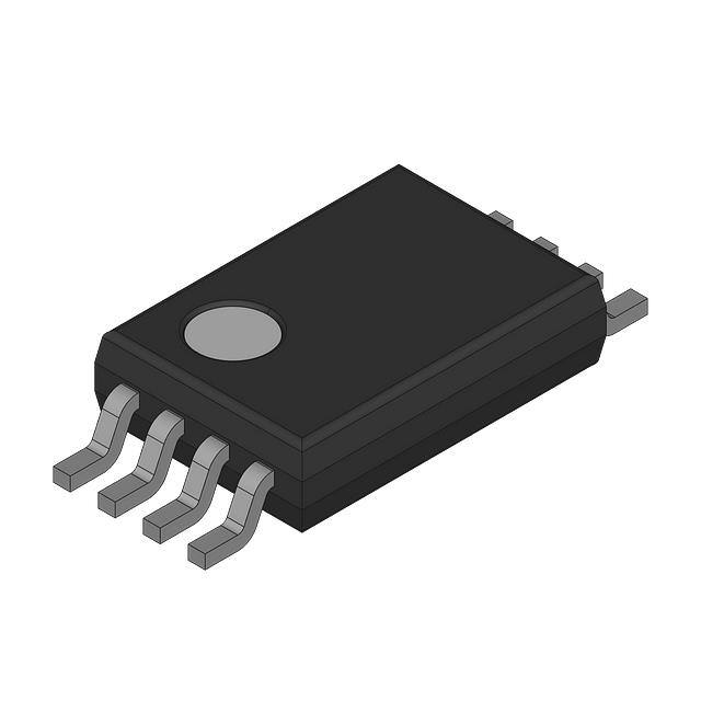
Figure 1. 8-Lead MSOP (RM-8)
ADR430/ADR431
ADR433/ADR434
ADR435
DNC
1
8
DNC
COMP
TOP VIEW
6 VOUT
(Not to Scale)
5 TRIM
GND 4
VIN 2
APPLICATIONS
7
NIC 3
Precision data acquisition systems
High resolution data converters
Medical instruments
Industrial process control systems
Optical control circuits
Precision instruments
NOTES
1. NIC = NOT INTERNALLY CONNECTED.
THIS PIN IS NOT CONNECTED INTERNALLY.
2. DNC = DO NOT CONNECT. DO NOT CONNECT TO THIS PIN.
04500-041
Data Sheet
Ultralow Noise XFET Voltage References
with Current Sink and Source Capability
ADR430/ADR431/ADR433/ADR434/ADR435
Figure 2. 8-Lead SOIC_N (R-8)
GENERAL DESCRIPTION
The ADR430/ADR431/ADR433/ADR434/ADR4351 series is a
family of XFET® voltage references featuring low noise, high
accuracy, and low temperature drift performance. Using Analog
Devices, Inc., temperature drift curvature correction and extra
implanted junction FET (XFET) technology, voltage change vs.
temperature nonlinearity in the ADR430/ADR431/ADR433/
ADR434/ADR435 is minimized.
The XFET references operate at lower current (800 µA) and
lower supply voltage headroom (2 V) than buried Zener
references. Buried Zener references require more than 5 V of
headroom for operation. The ADR430/ADR431/ADR433/
ADR434/ADR435 XFET references are low noise solutions for
5 V systems.
The ADR430/ADR431/ADR433/ADR434/ADR435 family has
the capability to source up to 30 mA of output current and sink
up to −20 mA. It also comes with a trim terminal to adjust the
output voltage over a ±0.5% range without compromising
performance.
1
The ADR430/ADR431/ADR433/ADR434/ADR435 are
available in 8-lead MSOP and 8-lead narrow SOIC packages. All
versions are specified over the extended industrial temperature
range of −40°C to +125°C.
Table 1. Selection Guide
Model
ADR430A
ADR430B
ADR431A
ADR431B
ADR433A
ADR433B
ADR434A
ADR434B
ADR435A
ADR435B
Output
Voltage (V)
2.048
2.048
2.500
2.500
3.000
3.000
4.096
4.096
5.000
5.000
Initial Accuracy
(mV)
±3
±1
±3
±1
±4
±1.5
±5
±1.5
±6
±2
Temperature
Coefficient
(ppm/°C)
10
3
10
3
10
3
10
3
10
3
Protected by U.S. Patent Number 5,838,192.
Rev. N
Document Feedback
Information furnished by Analog Devices is believed to be accurate and reliable. However, no
responsibility is assumed by Analog Devices for its use, nor for any infringements of patents or other
rights of third parties that may result from its use. Specifications subject to change without notice. No
license is granted by implication or otherwise under any patent or patent rights of Analog Devices.
Trademarks and registered trademarks are the property of their respective owners.
One Technology Way, P.O. Box 9106, Norwood, MA 02062-9106, U.S.A.
Tel: 781.329.4700 ©2003–2018 Analog Devices, Inc. All rights reserved.
Technical Support
www.analog.com
�ADR430/ADR431/ADR433/ADR434/ADR435
Data Sheet
TABLE OF CONTENTS
Features .............................................................................................. 1
Noise Performance ..................................................................... 16
Applications ....................................................................................... 1
High Frequency Noise ............................................................... 16
Pin Configurations ........................................................................... 1
Turn-On Settling Time .............................................................. 17
General Description ......................................................................... 1
Applications Information .............................................................. 18
Revision History ............................................................................... 2
Output Adjustment .................................................................... 18
Specifications..................................................................................... 4
ADR430 Electrical Characteristics............................................. 4
Reference for Converters in Optical Network Control
Circuits......................................................................................... 18
ADR431 Electrical Characteristics............................................. 5
High Voltage Floating Current Source .................................... 18
ADR433 Electrical Characteristics............................................. 6
Kelvin Connection ..................................................................... 18
ADR434 Electrical Characteristics............................................. 7
Dual Polarity References ........................................................... 19
ADR435 Electrical Characteristics............................................. 8
Programmable Current Source ................................................ 19
Absolute Maximum Ratings............................................................ 9
Programmable DAC Reference Voltage .................................. 20
Thermal Resistance ...................................................................... 9
Precision Voltage Reference for Data Converters .................. 20
ESD Caution .................................................................................. 9
Precision Boosted Output Regulator ....................................... 21
Pin Configurations and Function Descriptions ......................... 10
Outline Dimensions ....................................................................... 22
Typical Performance Characteristics ........................................... 11
Ordering Guide .......................................................................... 23
Theory of Operation ...................................................................... 16
Basic Voltage Reference Connections ...................................... 16
REVISION HISTORY
2/2018—Rev. M to Rev. N
Changed VO to VOUT and ADR43x to ADR430/ADR431/
ADR433/ADR434/ADR435 ......................................... Throughout
Changes to Figure 1, Figure 2, and General Description
Section ................................................................................................ 1
Changes to Output Current Capacity Parameter and Trim
Range Parameter, Table 2................................................................. 4
Changes to Output Current Capacity Parameter and Trim
Range Parameter, Table 3................................................................. 5
Changes to Output Current Capacity Parameter and Trim
Range Parameter, Table 4................................................................. 6
Changes to Output Current Capacity Parameter and Trim
Range Parameter, Table 5................................................................. 7
Changes to Output Current Capacity Parameter and Trim
Range Parameter, Table 6................................................................. 8
Added Pin Configuration and Function Descriptions Section,
Figure 3, Figure 4, and Table 9; Renumbered Sequentially ....... 10
Changes to Figure 14 and Figure 16 ............................................. 12
Changes to Figure 19 Caption and Figure 21 Caption .............. 13
Changes to Theory of Operation Section, Figure 32, Noise
Performance Section, and High Frequency Noise Section ....... 16
Changes to Figure 33 Caption, Figure 34, and Turn-On Settling
Time Section.................................................................................... 17
Changes to Reference for Converters in Optical Network
Control Circuits Section and Programmable Current Source
Section .............................................................................................. 19
Changes to Table 10 and Precision Boosted Output Regulator
Section.............................................................................................. 20
Changes to Precision Boosted Output Regulator Section......... 21
6/2015—Rev. L to Rev. M
Changes to Ordering Guide .......................................................... 22
7/2014—Rev. K to Rev. L
Changes to Default Conditions, Typical Performance
Characteristics Section .................................................................. 10
Changes to Ordering Guide .......................................................... 22
5/2014—Rev. J to Rev. K
Deleted ADR439 (Throughout) ......................................................1
Changes to Features Section and Table 1 .......................................1
Deleted Table 7; Renumbered Sequentially ...................................9
Changes to Ordering Guide .......................................................... 22
7/2011—Rev. I to Rev. J
Changes to Figure 1 and Figure 2 ....................................................1
Changes to Ordering Guide .......................................................... 23
5/2011—Rev. H to Rev. I
Added Endnote 1 in Table 2 .............................................................4
Added Endnote 1 in Table 3 .............................................................5
Added Endnote 1 in Table 4 .............................................................6
Rev. N | Page 2 of 23
�Data Sheet
ADR430/ADR431/ADR433/ADR434/ADR435
Added Endnote 1 in Table 5............................................................. 7
Added Endnote 1 in Table 6............................................................. 8
Added Endnote 1 in Table 7............................................................. 9
Deleted Negative Precision Reference Without Precision
Resistors Section ..............................................................................17
Deleted Figure 36; Renumbered Sequentially .............................18
2/2011—Rev. G to Rev. H
Updated Outline Dimensions ........................................................21
Changes to Ordering Guide ...........................................................22
7/2010—Rev. F to Rev. G
Changes to Storage Temperature Range in Table 9....................... 9
6/2010—Rev. E to Rev. F
Updated Pin Name NC to COMP Throughout ............................ 1
Changes to Figure 1 and Figure 2.................................................... 1
Changes to Figure 30 and High Frequency Noise Section ........15
Updated Outline Dimensions ........................................................21
Changes to Ordering Guide ...........................................................22
1/2009—Rev. D to Rev. E
Added High Frequency Noise Section and Equation 3;
Renumbered Sequentially ..............................................................15
Inserted Figure 31, Figure 32, and Figure 33; Renumbered
Sequentially ......................................................................................16
Changes to the Ordering Guide ....................................................22
12/2007—Rev. C to Rev. D
Changes to Initial Accuracy and Ripple Rejection Ratio
Parameters in Table 2 through Table 7 ........................................... 3
Changes to Table 9 ............................................................................ 9
Changes to Theory of Operation Section .................................... 15
Updated Outline Dimensions........................................................ 20
8/2006—Rev. B to Rev. C
Updated Format ................................................................. Universal
Changes to Table 1 ............................................................................ 1
Changes to Table 3 ............................................................................ 4
Changes to Table 4 ............................................................................ 5
Changes to Table 7 ............................................................................ 8
Changes to Figure 26 ...................................................................... 14
Changes to Figure 31 ...................................................................... 16
Updated Outline Dimensions........................................................ 20
Changes to Ordering Guide ........................................................... 21
9/2004—Rev. A to Rev. B
Added New Grade .............................................................. Universal
Changes to Specifications ................................................................ 3
Replaced Figure 3, Figure 4, Figure 5 ........................................... 10
Updated Ordering Guide ............................................................... 21
6/2004—Rev. 0 to Rev. A
Changes to Format ............................................................. Universal
Changes to the Ordering Guide .................................................... 20
12/2003—Revision 0: Initial Version
Rev. N | Page 3 of 23
�ADR430/ADR431/ADR433/ADR434/ADR435
Data Sheet
SPECIFICATIONS
ADR430 ELECTRICAL CHARACTERISTICS
VIN = 4.1 V to 18 V, IL = 0 mA, TA = 25°C, unless otherwise noted.
Table 2.
Parameter
OUTPUT VOLTAGE
A Grade
B Grade
INITIAL ACCURACY1
A Grade
Symbol
VOUT
Test Conditions/Comments
Min
Typ
Max
Unit
2.045
2.047
2.048
2.048
2.051
2.049
V
V
±3
±0.15
±1
±0.05
mV
%
mV
%
10
3
20
15
15
ppm/°C
ppm/°C
ppm/V
ppm/mA
ppm/mA
VOERR
B Grade
TEMPERATURE COEFFICIENT
A Grade
B Grade
LINE REGULATION
LOAD REGULATION
TCVOUT
OUTPUT CURRENT CAPACITY
Sourcing
Sinking
QUIESCENT CURRENT
VOLTAGE NOISE
VOLTAGE NOISE DENSITY
TURN-ON SETTLING TIME
LONG-TERM STABILITY2
OUTPUT VOLTAGE HYSTERESIS
RIPPLE REJECTION RATIO
SHORT CIRCUIT TO GND
SUPPLY VOLTAGE
OPERATING RANGE
SUPPLY VOLTAGE HEADROOM
TRIM RANGE
IL
1
2
∆VOUT/∆VIN
∆VOUT/∆IL
IIN
eN p-p
eN
tR
∆VOUT
VOUT_HYS
RRR
ISC
VIN
−40°C < TA < +125°C
−40°C < TA < +125°C
VIN = 4.1 V to 18 V, −40°C < TA < +125°C
IL = 0 mA to 10 mA, VIN = 5.0 V, −40°C < TA < +125°C
IL = −10 mA to 0 mA, VIN = 5.0 V, −40°C < TA < +125°C
2
1
5
30
−20
560
3.5
60
10
40
20
–70
40
No load, −40°C < TA < +125°C
0.1 Hz to 10.0 Hz
1 kHz
CL = 0 µF
1000 hours
fIN = 1 kHz
4.1
VIN − VOUT
2
−5
18
mA
mA
µA
µV p-p
nV/√Hz
µs
ppm
ppm
dB
mA
V
+5
V
%
800
Initial accuracy does not include shift due to solder heat effect.
The long-term stability specification is noncumulative. The drift in subsequent 1000 hour periods is significantly lower than in the first 1000 hour period.
Rev. N | Page 4 of 23
�Data Sheet
ADR430/ADR431/ADR433/ADR434/ADR435
ADR431 ELECTRICAL CHARACTERISTICS
VIN = 4.5 V to 18 V, IL = 0 mA, TA = 25°C, unless otherwise noted.
Table 3.
Parameter
OUTPUT VOLTAGE
A Grade
B Grade
INITIAL ACCURACY1
A Grade
Symbol
VOUT
Test Conditions/Comments
Min
Typ
Max
Unit
2.497
2.499
2.500
2.500
2.503
2.501
V
V
±3
±0.12
±1
±0.04
mV
%
mV
%
10
3
20
15
15
ppm/°C
ppm/°C
ppm/V
ppm/mA
ppm/mA
VOERR
B Grade
TEMPERATURE COEFFICIENT
A Grade
B Grade
LINE REGULATION
LOAD REGULATION
OUTPUT CURRENT CAPACITY
Sourcing
Sinking
QUIESCENT CURRENT
VOLTAGE NOISE
VOLTAGE NOISE DENSITY
TURN-ON SETTLING TIME
LONG-TERM STABILITY2
OUTPUT VOLTAGE HYSTERESIS
RIPPLE REJECTION RATIO
SHORT CIRCUIT TO GND
SUPPLY VOLTAGE
OPERATING RANGE
SUPPLY VOLTAGE HEADROOM
TRIM RANGE
1
2
TCVOUT
∆VOUT/∆VIN
∆VOUT/∆IL
−40°C < TA < +125°C
−40°C < TA < +125°C
VIN = 4.5 V to 18 V, −40°C < TA < +125°C
IL = 0 mA to 10 mA, VIN = 5.0 V, −40°C < TA < +125°C
IL = −10 mA to 0 mA, VIN = 5.0 V, −40°C < TA < +125°C
2
1
5
IL
IIN
eN p-p
eN
tR
∆VOUT
VOUT_HYS
RRR
ISC
VIN
30
−20
580
3.5
80
10
40
20
−70
40
4.5
18
mA
mA
µA
µV p-p
nV/√Hz
µs
ppm
ppm
dB
mA
V
2
−5
+5
V
%
No load, −40°C < TA < +125°C
0.1 Hz to 10.0 Hz
1 kHz
CL = 0 µF
1000 hours
fIN = 1 kHz
VIN − VOUT
800
Initial accuracy does not include shift due to solder heat effect.
The long-term stability specification is noncumulative. The drift in subsequent 1000 hour periods is significantly lower than in the first 1000 hour period.
Rev. N | Page 5 of 23
�ADR430/ADR431/ADR433/ADR434/ADR435
Data Sheet
ADR433 ELECTRICAL CHARACTERISTICS
VIN = 5.0 V to 18 V, IL = 0 mA, TA = 25°C, unless otherwise noted.
Table 4.
Parameter
OUTPUT VOLTAGE
A Grade
B Grade
INITIAL ACCURACY1
A Grade
Symbol
VOUT
Test Conditions/Comments
Min
Typ
Max
Unit
2.996
2.9985
3.000
3.000
3.004
3.0015
V
V
±4
±0.13
±1.5
±0.05
mV
%
mV
%
10
3
20
15
15
ppm/°C
ppm/°C
ppm/V
ppm/mA
ppm/mA
VOERR
B Grade
TEMPERATURE COEFFICIENT
A Grade
B Grade
LINE REGULATION
LOAD REGULATION
TCVOUT
OUTPUT CURRENT CAPACITY
Sourcing
Sinking
QUIESCENT CURRENT
VOLTAGE NOISE
VOLTAGE NOISE DENSITY
TURN-ON SETTLING TIME
LONG-TERM STABILITY2
OUTPUT VOLTAGE HYSTERESIS
RIPPLE REJECTION RATIO
SHORT CIRCUIT TO GND
SUPPLY VOLTAGE
OPERATING RANGE
SUPPLY VOLTAGE HEADROOM
TRIM RANGE
IL
1
2
∆VOUT/∆VIN
∆VOUT/∆IL
IIN
eN p-p
eN
tR
∆VOUT
VOUT_HYS
RRR
ISC
VIN
−40°C < TA < +125°C
−40°C < TA < +125°C
VIN = 5 V to 18 V, −40°C < TA < +125°C
IL = 0 mA to 10 mA, VIN = 6 V, −40°C < TA < +125°C
IL = −10 mA to 0 mA, VIN = 6 V, −40°C < TA < +125°C
2
1
5
30
−20
590
3.75
90
10
40
20
−70
40
5.0
18
mA
mA
µA
µV p-p
nV/√Hz
µs
ppm
ppm
dB
mA
V
2
−5
+5
V
%
No load, −40°C < TA < +125°C
0.1 Hz to 10.0 Hz
1 kHz
CL = 0 µF
1000 hours
fIN = 1 kHz
VIN − VOUT
800
Initial accuracy does not include shift due to solder heat effect.
The long-term stability specification is noncumulative. The drift in subsequent 1000 hour periods is significantly lower than in the first 1000 hour period.
Rev. N | Page 6 of 23
�Data Sheet
ADR430/ADR431/ADR433/ADR434/ADR435
ADR434 ELECTRICAL CHARACTERISTICS
VIN = 6.1 V to 18 V, IL = 0 mA, TA = 25°C, unless otherwise noted.
Table 5.
Parameter
OUTPUT VOLTAGE
A Grade
B Grade
INITIAL ACCURACY1
A Grade
Symbol
VOUT
Test Conditions/Comments
Min
Typ
Max
Unit
4.091
4.0945
4.096
4.096
4.101
4.0975
V
V
±5
±0.12
±1.5
±0.04
mV
%
mV
%
10
3
20
15
15
ppm/°C
ppm/°C
ppm/V
ppm/mA
ppm/mA
VOERR
B Grade
TEMPERATURE COEFFICIENT
A Grade
B Grade
LINE REGULATION
LOAD REGULATION
OUTPUT CURRENT CAPACITY
Sourcing
Sinking
QUIESCENT CURRENT
VOLTAGE NOISE
VOLTAGE NOISE DENSITY
TURN-ON SETTLING TIME
LONG-TERM STABILITY2
OUTPUT VOLTAGE HYSTERESIS
RIPPLE REJECTION RATIO
SHORT CIRCUIT TO GND
SUPPLY VOLTAGE
OPERATING RANGE
SUPPLY VOLTAGE HEADROOM
TRIM RANGE
1
2
TCVOUT
∆VOUT/∆VIN
∆VOUT/∆IL
−40°C < TA < +125°C
−40°C < TA < +125°C
VIN = 6.1 V to 18 V, −40°C < TA < +125°C
IL = 0 mA to 10 mA, VIN = 7 V, −40°C < TA < +125°C
IL = −10 mA to 0 mA, VIN = 7 V, −40°C < TA < +125°C
2
1
5
IL
IIN
eN p-p
eN
tR
∆VOUT
VOUT_HYS
RRR
ISC
VIN
30
−20
595
6.25
100
10
40
20
−70
40
6.1
18
mA
mA
µA
µV p-p
nV/√Hz
µs
ppm
ppm
dB
mA
V
2
−5
+5
V
%
No load, −40°C < TA < +125°C
0.1 Hz to 10.0 Hz
1 kHz
CL = 0 µF
1000 hours
fIN = 1 kHz
VIN − VOUT
800
Initial accuracy does not include shift due to solder heat effect.
The long-term stability specification is noncumulative. The drift in subsequent 1000 hour periods is significantly lower than in the first 1000 hour period.
Rev. N | Page 7 of 23
�ADR430/ADR431/ADR433/ADR434/ADR435
Data Sheet
ADR435 ELECTRICAL CHARACTERISTICS
VIN = 7.0 V to 18 V, IL = 0 mA, TA = 25°C, unless otherwise noted.
Table 6.
Parameter
OUTPUT VOLTAGE
A Grade
B Grade
INITIAL ACCURACY1
A Grade
Symbol
VOUT
Test Conditions/Comments
Min
Typ
Max
Unit
4.994
4.998
5.000
5.000
5.006
5.002
V
V
±6
±0.12
±2
±0.04
mV
%
mV
%
10
3
20
15
15
ppm/°C
ppm/°C
ppm/V
ppm/mA
ppm/mA
VOERR
B Grade
TEMPERATURE COEFFICIENT
A Grade
B Grade
LINE REGULATION
LOAD REGULATION
TCVOUT
OUTPUT CURRENT CAPACITY
Sourcing
Sinking
QUIESCENT CURRENT
VOLTAGE NOISE
VOLTAGE NOISE DENSITY
TURN-ON SETTLING TIME
LONG-TERM STABILITY2
OUTPUT VOLTAGE HYSTERESIS
RIPPLE REJECTION RATIO
SHORT CIRCUIT TO GND
SUPPLY VOLTAGE OPERATING RANGE
SUPPLY VOLTAGE HEADROOM
TRIM RANGE
IL
1
2
∆VOUT/∆VIN
∆VOUT/∆IL
IIN
eN p-p
eN
tR
∆VOUT
VOUT_HYS
RRR
ISC
VIN
VIN − VOUT
−40°C < TA < +125°C
−40°C < TA < +125°C
VIN = 7 V to 18 V, −40°C < TA < +125°C
IL = 0 mA to 10 mA, VIN = 8 V, −40°C < TA < +125°C
IL = −10 mA to 0 mA, VIN = 8 V, −40°C < TA < +125°C
2
1
5
30
−20
620
8
115
10
40
20
−70
40
No load, −40°C < TA < +125°C
0.1 Hz to 10 Hz
1 kHz
CL = 0 µF
1000 hours
fIN = 1 kHz
7.0
2
−5
800
18
+5
Initial accuracy does not include shift due to solder heat effect.
The long-term stability specification is noncumulative. The drift in subsequent 1000 hour periods is significantly lower than in the first 1000 hour period.
Rev. N | Page 8 of 23
mA
mA
µA
µV p-p
nV/√Hz
µs
ppm
ppm
dB
mA
V
V
%
�Data Sheet
ADR430/ADR431/ADR433/ADR434/ADR435
ABSOLUTE MAXIMUM RATINGS
TA = 25°C, unless otherwise noted.
THERMAL RESISTANCE
Table 7.
θJA is specified for the worst case conditions, that is, a device
soldered in a circuit board for surface-mount packages.
Parameter
Supply Voltage
Output Short-Circuit Duration to GND
Storage Temperature Range
Operating Temperature Range
Junction Temperature Range
Lead Temperature, Soldering (60 sec)
Rating
20 V
Indefinite
−65°C to +150°C
−40°C to +125°C
−65°C to +150°C
300°C
Stresses at or above those listed under Absolute Maximum
Ratings may cause permanent damage to the product. This is a
stress rating only; functional operation of the product at these
or any other conditions above those indicated in the operational
section of this specification is not implied. Operation beyond
the maximum operating conditions for extended periods may
affect product reliability.
Table 8. Thermal Resistance
Package Type
8-Lead SOIC_N (R)
8-Lead MSOP (RM)
ESD CAUTION
Rev. N | Page 9 of 23
θJA
130
142
θJC
43
44
Unit
°C/W
°C/W
�ADR430/ADR431/ADR433/ADR434/ADR435
Data Sheet
PIN CONFIGURATIONS AND FUNCTION DESCRIPTIONS
ADR430/ADR431
ADR433/ADR434
ADR435
ADR430/ADR431
ADR433/ADR434
ADR435
DNC
7
COMP
NIC 3
TOP VIEW
(Not to Scale)
GND 4
6
VOUT
5
TRIM
NOTES
1. NIC = NOT INTERNALLY CONNECTED.
THIS PIN IS NOT CONNECTED INTERNALLY.
2. DNC = DO NOT CONNECT. DO NOT CONNECT TO THIS PIN.
DNC
1
8
DNC
COMP
TOP VIEW
6 VOUT
(Not to Scale)
5 TRIM
GND 4
VIN 2
7
NIC 3
NOTES
1. NIC = NOT INTERNALLY CONNECTED.
THIS PIN IS NOT CONNECTED INTERNALLY.
2. DNC = DO NOT CONNECT. DO NOT CONNECT TO THIS PIN.
Figure 3. 8-Lead MSOP Pin Configuration
04500-141
8
VIN 2
04500-101
DNC 1
Figure 4. 8-Lead SOIC Pin Configuration
Table 9. Pin Function Descriptions
Pin No.
1
2
3
4
5
6
7
8
Mnemonic
DNC
VIN
NIC
GND
TRIM
VOUT
COMP
DNC
Description
Do Not Connect. Do not connect to this pin.
Input Voltage Connection.
Not Internally Connected. This pin is not connected internally.
Ground.
Output Voltage Trim.
Output Voltage.
Compensation Input. Connect a series resistor and capacitor network from COMP to VOUT to reduce overall noise.
Do Not Connect. Do not connect to this pin.
Rev. N | Page 10 of 23
�Data Sheet
ADR430/ADR431/ADR433/ADR434/ADR435
TYPICAL PERFORMANCE CHARACTERISTICS
Default conditions: VIN = 7 V, TA = 25°C, CIN = COUT = 0.1 μF, unless otherwise noted.
0.8
2.5009
SUPPLY CURRENT (mA)
OUTPUT VOLTAGE (V)
2.5007
2.5005
2.5003
2.5001
2.4999
0.7
+125°C
0.6
+25°C
–40°C
0.5
0.4
2.4997
20
35
50
65
80
95
110
125
TEMPERATURE (°C)
4
8
10
12
14
16
125
18
INPUT VOLTAGE (V)
Figure 5. ADR431 Output Voltage vs. Temperature
Figure 8. ADR435 Supply Current vs. Input Voltage
4.0980
700
4.0975
650
SUPPLY CURRENT (µA)
OUTPUT VOLTAGE (V)
6
04500-018
5
04500-019
–10
04500-020
0.3
–25
04500-015
2.4995
–40
4.0970
4.0965
4.0960
4.0955
600
550
500
450
–25
–10
5
20
35
50
65
80
95
110
TEMPERATURE (°C)
125
400
–40
04500-016
4.0950
–40
–25
–10
5
20
35
50
65
80
95
110
TEMPERATURE (°C)
Figure 6. ADR434 Output Voltage vs. Temperature
Figure 9. ADR435 Supply Current vs. Temperature
0.60
5.0025
+125°C
0.58
5.0020
SUPPLY CURRENT (mA)
5.0010
5.0005
5.0000
0.54
0.52
+25°C
0.50
0.48
0.46
–40°C
0.44
4.9995
0.42
4.9990
–40
0.40
–25
–10
5
20
35
50
65
80
95
110
TEMPERATURE (°C)
125
04500-017
OUTPUT VOLTAGE (V)
0.56
5.0015
Figure 7. ADR435 Output Voltage vs. Temperature
6
8
10
12
14
16
INPUT VOLTAGE (V)
Figure 10. ADR431 Supply Current vs. Input Voltage
Rev. N | Page 11 of 23
�ADR430/ADR431/ADR433/ADR434/ADR435
Data Sheet
2.5
SUPPLY VOLTAGE HEADROOM (V)
SUPPLY CURRENT (µA)
580
550
520
490
460
400
–40
–25
–10
5
20
35
50
65
80
95
110
125
TEMPERATURE (°C)
–40°C
1.5
+25°C
1.0
+125°C
0.5
0
–10
04500-021
430
2.0
–5
0
5
10
LOAD CURRENT (mA)
Figure 11. ADR431 Supply Current vs. Temperature
04500-024
610
Figure 14. ADR431 Supply Voltage Headroom vs. Load Current over
Temperature
15
1.9
IL = 0mA to 10mA
NO LOAD
12
MINIMUM HEADROOM (V)
LOAD REGULATION (ppm/mA)
1.8
9
6
1.7
1.6
1.5
1.4
1.3
1.2
3
–25
–10
5
20
35
50
65
80
95
110
125
TEMPERATURE (°C)
1.0
–40
04500-022
0
–40
–25
–10
5
20
35
50
65
80
95
110
125
TEMPERATURE (°C)
Figure 12. ADR431 Load Regulation vs. Temperature
04500-025
1.1
Figure 15. ADR431 Minimum Headroom vs. Temperature
2.5
15
9
6
3
0
–40
–25
–10
5
20
35
50
65
80
95
110
TEMPERATURE (°C)
125
2.0
–40°C
1.5
+25°C
1.0
+125°C
0.5
0
–10
–5
0
LOAD CURRENT (mA)
Figure 13. ADR435 Load Regulation vs. Temperature
5
10
04500-026
SUPPLY VOLTAGE HEADROOM (V)
12
04500-023
LOAD REGULATION (ppm/mA)
IL = 0mA to 10mA
Figure 16. ADR435 Supply Voltage Headroom vs. Load Current over
Temperature
Rev. N | Page 12 of 23
�Data Sheet
ADR430/ADR431/ADR433/ADR434/ADR435
1.9
NO LOAD
MINIMUM HEADROOM (V)
1.7
CL = 0.01µF
NO INPUT CAPACITOR
VOUT = 1V/DIV
1.5
1.3
1.1
–25
–10
5
20
35
50
65
80
95
110
125
TEMPERATURE (°C)
TIME = 4µs/DIV
04500-027
0.9
–40
Figure 17. ADR435 Minimum Headroom vs. Temperature
04500-031
VIN = 2V/DIV
Figure 20. ADR431 Turn-On Response Settling Time, 0.01 µF Load Capacitor
20
VIN = 7V TO 18V
VOUT = 1V/DIV
12
CIN = 0.01µF
NO LOAD
8
4
0
–25
–10
5
20
35
50
65
80
95
110
125
TEMPERATURE (°C)
04500-028
–4
–40
TIME = 4µs/DIV
04500-032
VIN = 2V/DIV
Figure 21. ADR431 Turn-Off Settling Time Response
Figure 18. ADR435 Line Regulation vs. Temperature
CIN = 0.01µF
NO LOAD
BYPASS CAPACITOR = 0µF
LINE
INTERRUPTION
VOUT = 1V/DIV
VIN = 500mV/DIV
VOUT = 50mV/DIV
TIME = 4µs/DIV
TIME = 100µs/DIV
Figure 22. ADR431 Line Transient Response
Figure 19. ADR431 Turn-On Settling Time Response, No Load
Rev. N | Page 13 of 23
04500-033
VIN = 2V/DIV
04500-030
LINE REGULATION (ppm/V)
16
�ADR430/ADR431/ADR433/ADR434/ADR435
BYPASS CAPACITOR = 0.1µF
Data Sheet
LINE
INTERRUPTION
VIN = 500mV/DIV
VOUT = 50mV/DIV
TIME = 1s/DIV
Figure 23. ADR431 Line Transient Response, 0.1 µF Bypass Capacitor
04500-037
TIME = 100µs/DIV
04500-034
2µV/DIV
Figure 26. ADR435 0.1 Hz to 10.0 Hz Voltage Noise
1µV/DIV
TIME = 1s/DIV
Figure 24. ADR431 0.1 Hz to 10.0 Hz Voltage Noise
04500-038
TIME = 1s/DIV
04500-035
50µV/DIV
Figure 27. ADR435 10 Hz to 10 kHz Voltage Noise
14
NUMBER OF PARTS
12
10
8
6
4
50µV/DIV
0
–110 –90
04500-036
TIME = 1s/DIV
–70
–50
–30
–10
10
30
50
DEVIATION (PPM)
Figure 25. ADR431 10 Hz to 10 kHz Voltage Noise
Figure 28. ADR431 Typical Hysteresis
Rev. N | Page 14 of 23
70
90
110
04500-029
2
�Data Sheet
ADR430/ADR431/ADR433/ADR434/ADR435
10
50
45
–10
RIPPLE REJECTION (dB)
35
30
25
ADR435
20
15
ADR433
–30
–50
–70
–90
–110
10
ADR430
5
–150
1k
10k
FREQUENCY (Hz)
100k
10
100
1k
10k
100k
FREQUENCY (Hz)
Figure 29. Output Impedance vs. Frequency
Figure 30. Ripple Rejection vs. Frequency
Rev. N | Page 15 of 23
1M
04500-040
0
100
–130
04500-039
OUTPUT IMPEDANCE (Ω)
40
�ADR430/ADR431/ADR433/ADR434/ADR435
Data Sheet
THEORY OF OPERATION
The ADR430/ADR431/ADR433/ADR434/ADR435 series of
references uses a reference generation technique known as XFET.
This technique yields a reference with low supply current,
optimal thermal hysteresis, and exceptionally low noise. The
core of the XFET reference consists of two junction field effect
transistors (JFETs), one of which has an extra channel implant
to raise its pinch off voltage. The two JFETs run at the same
drain current, and the difference in pinch off voltage is
amplified to form a highly stable voltage reference.
When these devices are used in applications at higher currents,
use the following equation to account for the temperature
effects due to the power dissipation increases:
The intrinsic reference voltage is around 0.5 V with a negative
temperature coefficient of about −120 ppm/°C. This slope is
essentially constant to the dielectric constant of silicon and can
be compensated closely by adding a correction term generated
in the same fashion as the proportional to absolute temperature
(PTAT) term used to compensate band gap references. The
primary advantage of an XFET reference is its correction term,
which is ~30 times lower and requires less correction than that of
a band gap reference. Because most of the noise of a band gap
reference comes from the temperature compensation circuitry,
the XFET results in much lower noise.
BASIC VOLTAGE REFERENCE CONNECTIONS
TJ = PD × θJA + TA
where:
TJ and TA are the junction and ambient temperatures, respectively.
PD is the device power dissipation.
θJA is the device package junction to ambient thermal resistance.
Voltage references, in general, require a bypass capacitor connected
from VOUT to ground. The circuit in Figure 32 shows the basic
configuration for the ADR430/ADR431/ADR433/ADR434/
ADR435 family of references. Other than a 0.1 µF capacitor at
the output to help improve noise suppression, a large output
capacitor at the output is not required for circuit stability.
ADR430/ADR431
ADR433/ADR434
ADR435
The ADR430/ADR431/ADR433/ADR434/ADR435 devices are
created by on-chip adjustment of R2 and R3 to achieve 2.048 V to
5.000 V at the reference output.
VIN
I1
I1
ADR43x
IPTAT
+
0.1µF
NIC
GND
8
DNC
COMP
VOUT
TOP VIEW
6
3
(Not to Scale)
4
5 TRIM
2
10µF
7
NOTES
1. NIC = NOT INTERNALLY CONNECTED.
THIS PIN IS NOT CONNECTED INTERNALLY.
2. DNC = DO NOT CONNECT. DO NOT CONNECT TO THIS PIN.
(1)
where:
G is the gain of the reciprocal of the divider ratio.
∆VP is the difference in pinch-off voltage between the two JFETs.
R1 is a resistor, as shown in Figure 31.
IPTAT is the positive temperature coefficient correction current.
1
0.1µF
04500-044
DNC
VIN
Figure 31 shows the basic topology of the ADR430/ADR431/
ADR433/ADR434/ADR435 series. The temperature correction
term is provided by a current source with a value designed to be
PTAT. The general equation is
VOUT = G (ΔVP – R1 × IPTAT)
(2)
Figure 32. Basic Voltage Reference Configuration
NOISE PERFORMANCE
The noise generated by the ADR430, ADR431, and ADR433
family of references is typically less than or equal to 3.75 µV p-p
over the 0.1 Hz to 10.0 Hz band for. Figure 24 shows the 0.1 Hz
to 10.0 Hz noise of the ADR431, which is only 3.5 µV p-p. The
noise measurement is made with a band-pass filter composed of
a two-pole, high-pass filter with a corner frequency at 0.1 Hz
and a two-pole, low-pass filter with a corner frequency at 10.0 Hz.
HIGH FREQUENCY NOISE
VOUT
The total noise generated by the ADR430/ADR431/ADR433/
ADR434/ADR435 family of references is composed of the
reference noise and the op amp noise. Figure 33 shows the
wideband noise from 10 Hz to 25 kHz. An internal node of the op
amp is available on Pin 7, and by overcompensating the op amp,
the overall noise can be reduced.
R2
*
R1
*EXTRA CHANNEL IMPLANT
VOUT = G(ΔVP – R1 × IPTAT)
R3
GND
04500-002
ΔVP
Figure 31. Simplified Schematic Device Power Dissipation Considerations
The ADR430/ADR431/ADR433/ADR434/ADR435 family of
references is guaranteed to deliver load currents up to 10 mA
with an input voltage that ranges from 4.1 V to 18 V.
Consider that, in a closed-loop configuration, the effective
output impedance of an op amp is as follows:
RO =
rO
1 + AVO β
where:
RO is the apparent output impedance.
rO is the output resistance of the op amp.
Rev. N | Page 16 of 23
(3)
�ADR430/ADR431/ADR433/ADR434/ADR435
However, references are used increasingly to drive the reference
input of an analog-to-digital (ADC) that may present a dynamic,
switching capacitive load. Large capacitors, in the microfarad range,
reduce the change in reference voltage to less than one-half LSB.
Figure 33 shows the ADR431 noise spectrum with various
capacitive values to 50 µF. With no capacitive load, the noise
spectrum is relatively flat at approximately 60 nV/√Hz to
70 nV/√Hz. With various values of capacitive loading, the
predicted noise peaking becomes evident.
1000
ADR431
NO COMPENSATION
CL = 1µF
DNC
VIN
+
10µF
0.1µF
NIC
GND
1
8
2
7
DNC
COMP 82kΩ
VOUT
TOP VIEW
6
(Not to Scale)
4
5 TRIM
10nF
3
0.1µF
NOTES
1. NIC = NOT INTERNALLY CONNECTED.
THIS PIN IS NOT CONNECTED INTERNALLY.
2. DNC = DO NOT CONNECT. DO NOT CONNECT TO THIS PIN.
Figure 34. Compensated Reference
The 82 kΩ resistor and 10 nF capacitor eliminate noise peaking
(see Figure 35). Leave the COMP pin unconnected if unused.
100
CL = 10µF
RC 82kΩ AND 10nF
CL = 1µF
RC 82kΩ AND 10nF
CL = 50µF
RC 82kΩ AND 10nF
10
10
CL = 50µF
100
100
1k
FREQUENCY (Hz)
10k
Figure 35. Noise with Compensation Network
CL = 0µF
10
10
100
1k
FREQUENCY (Hz)
10k
TURN-ON SETTLING TIME
100k
04500-042
NOISE DENSITY (nV/√Hz)
CL = 10µF
ADR430/ADR431
ADR433/ADR434
ADR435
04500-003
Equation 3 shows that the apparent output impedance is
approximately reduced by the excess loop gain; therefore, as the
frequency increases, the excess loop gain decreases, and the
apparent output impedance increases. A passive element whose
impedance increases as its frequency increases is an inductor.
When a capacitor is added to the output of an op amp or a
reference, it forms a tuned circuit that resonates at a certain
frequency and results in gain peaking. Gain peaking can be
observed by using a model of an op amp with a single-pole
response and some pure resistance in series with the output.
Changing capacitive loads results in peaking at different
frequencies. For most normal op amp applications with low
capacitive loading (


 工商网监
湘ICP备2023018690号
工商网监
湘ICP备2023018690号
