100 MHz to 30 GHz,
Silicon, SP4T Switch
ADRF5044
Data Sheet
GND
GND
RF2
GND
23
22
21
20
19
1
ADRF5044
18
GND
GND
2
50Ω 50Ω
17
VDD
RFC
3
16
V1
GND
4
15
V2
GND
5
14
VSS
13
GND
DRIVER
GND
9
10
11
12
GND
8
RF3
7
GND
6
GND
GND
50Ω
16313-001
50Ω
RF4
Test instrumentation
Microwave radios and very small aperture terminals (VSATs)
Military radios, radars, and electronic counter measures (ECMs)
Broadband telecommunications systems
24
GND
APPLICATIONS
RF1
FUNCTIONAL BLOCK DIAGRAM
Ultrawideband frequency range: 100 MHz to 30 GHz
Nonreflective 50 Ω design
Low insertion loss: 2.6 dB at 20 GHz to 30 GHz
High isolation: 43 dB at 20 GHz to 30 GHz
High input linearity
P1dB: 28 dBm typical
IP3: 50 dBm typical
High power handling
24 dBm through path
24 dBm terminated path
No low frequency spurious
0.1 dB settling time (50% VCTL to 0.1 dB of final RF output): 37 ns
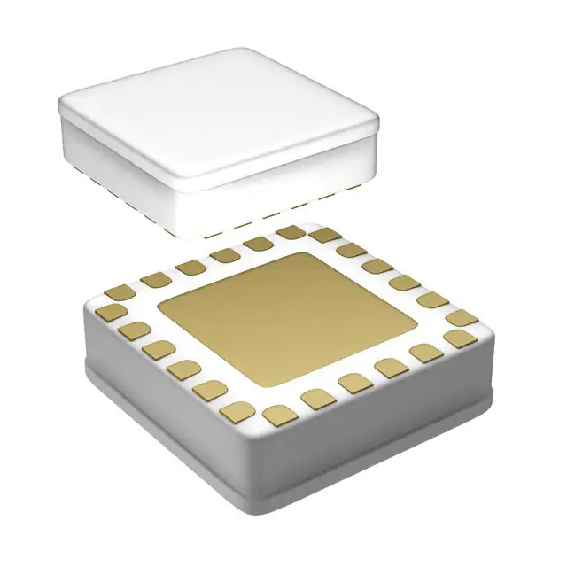
24-terminal LGA package
GND
FEATURES
Figure 1.
GENERAL DESCRIPTION
The ADRF5044 is a general-purpose, single-pole, four-throw
(SP4T) switch manufactured using a silicon process. It comes
in a 24-terminal land grid array (LGA) package and provides
high isolation and low insertion loss from 100 MHz to 30 GHz.
Rev. A
This broadband switch requires dual-supply voltages, +3.3 V and
−3.3 V, and provides complementary metal-oxide semiconductor
(CMOS)/low voltage transistor-transistor logic (LVTTL) logiccompatible control.
Document Feedback
Information furnished by Analog Devices is believed to be accurate and reliable. However, no
responsibility is assumed by Analog Devices for its use, nor for any infringements of patents or other
rights of third parties that may result from its use. Specifications subject to change without notice.
No license is granted by implication or otherwise under any patent or patent rights of Analog
Devices. Trademarks and registered trademarks are the property of their respective owners.
One Technology Way, P.O. Box 9106, Norwood, MA 02062-9106, U.S.A.
Tel: 781.329.4700 ©2017–2020 Analog Devices, Inc. All rights reserved.
Technical Support
www.analog.com
�ADRF5044
Data Sheet
TABLE OF CONTENTS
Features .............................................................................................. 1
Typical Performance Characteristics .............................................7
Applications ...................................................................................... 1
Insertion Loss, Return Loss, and Isolation ................................7
Functional Block Diagram .............................................................. 1
General Description ......................................................................... 1
Input 0.1 dB, 1 dB Power Compression, and Third-Order
Intercept .........................................................................................9
Revision History ............................................................................... 2
Theory of Operation ...................................................................... 10
Specifications .................................................................................... 3
Applications Information ............................................................. 11
Absolute Maximum Ratings ........................................................... 5
Evaluation Board ........................................................................ 11
Thermal Resistance ...................................................................... 5
Probe Matrix Board ................................................................... 13
Power Derating Curves ............................................................... 5
Outline Dimensions ....................................................................... 14
ESD Caution.................................................................................. 5
Ordering Guide .......................................................................... 14
Pin Configuration and Function Descriptions ............................ 6
Interface Schematics .................................................................... 6
REVISION HISTORY
3/2020—Rev. 0 to Rev. A
Changes to Digital Control Inputs Parameter, Table 2 .............. 5
Added Endnote 1, Table 2; Renumbered Sequentially ............... 5
Changes to Theory of Operation Section.................................... 10
12/2017—Revision 0: Initial Version
Rev. A | Page 2 of 14
�Data Sheet
ADRF5044
SPECIFICATIONS
VDD = 3.3 V, VSS = −3.3 V, V1 = 0 V or 3.3 V, V2 = 0 V or 3.3 V, and TCASE = 25°C, 50 Ω system, unless otherwise noted.
Table 1.
Parameter
FREQUENCY RANGE
INSERTION LOSS
Between RFC and RF1 to RF4 (On) (Worst Case)
Symbol
ISOLATION
Between RFC and RF1 to RF4 (Off) (Worst Case)
RETURN LOSS
RFC and RF1 to RF4 (On)
RF1 to RF4 (Off)
SWITCHING TIME
Rise and Fall
On and Off
Settling
0.1 dB
0.05 dB
INPUT LINEARITY
Power Compression
0.1 dB
1 dB
Third-Order Intercept
P0.1dB
P1dB
IP3
SUPPLY CURRENT
Positive
IDD
Negative
DIGITAL CONTROL INPUTS
Voltage
Low
High
Current
Low and High
RECOMMENDED OPERATING CONDITONS
Supply Voltage
Positive
Negative
Digital Control Voltage
tRISE, tFALL
tON, tOFF
ISS
Test Conditions/Comments
Min
100
Typ
Max
30,000
Unit
MHz
100 MHz to 10 GHz
10 GHz to 20 GHz
20 GHz to 30 GHz
1.7
2.1
2.6
dB
dB
dB
100 MHz to 10 GHz
10 GHz to 20 GHz
20 GHz to 30 GHz
55
52
43
dB
dB
dB
100 MHz to 10 GHz
10 GHz to 20 GHz
20 GHz to 30 GHz
100 MHz to 10 GHz
10 GHz to 20 GHz
20 GHz to 30 GHz
16
22
22
24
24
16
dB
dB
dB
dB
dB
dB
10% to 90% of radio frequency (RF) output
50% VCTL to 90% of RF output
4
19
ns
ns
50% VCTL to 0.1 dB of final RF output
50% VCTL to 0.05 dB of final RF output
37
50
ns
ns
26
28
50
dBm
dBm
dBm
Two-tone input power = 14 dBm each tone,
Δf = 1 MHz
VDD, VSS pins
Typical at VCTL = 0 V or 3.3 V, maximum at
VCTL = 0.8 V or 1.4 V
Typical at VCTL = 0 V or 3.3 V, maximum at
VCTL = 0.8 V or 1.4 V
V1, V2 pins
VINL
VINH
12
20
μA
110
130
μA
0.8
3.3
V
V
0
1.2
IINL, IINH
很抱歉,暂时无法提供与“ADRF5044BCCZN”相匹配的价格&库存,您可以联系我们找货
免费人工找货