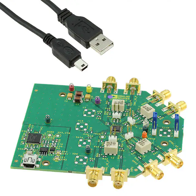
31 MHz, Dual Programmable Filters
and Variable Gain Amplifiers
ADRF6516
Data Sheet
FUNCTIONAL BLOCK DIAGRAM
Matched pair of programmable filters and VGAs
Continuous gain control range: 50 dB
Digital gain control: 15 dB
6-pole Butterworth filter: 1 MHz to 31 MHz
in 1 MHz steps, 1 dB corner frequency
Preamplifier and postamplifier gain steps
IMD3: >65 dBc for 1.5 V p-p composite output
HD2, HD3: >65 dBc for 1.5 V p-p output
Differential input and output
Flexible output and input common-mode ranges
Optional dc offset compensation loop
SPI programmable filter corners and gain steps
Power-down feature
Single 3.3 V supply operation
APPLICATIONS
ENBL INP1
VPS
COM VICM OFS1 VPS
VPSD
OPP1
COMD
OPM1
LE
COM
CLK
GAIN
SPI
DATA
VOCM
SDO
COM
COM
OPM2
VPS
ADRF6516
COM
Baseband IQ receivers
Diversity receivers
ADC drivers
Point-to-point and point-to-multipoint radio
Instrumentation
Medical
INM1
INP2
INM2
VPS
COM OFDS OFS2 VPS
OPP2
09422-001
FEATURES
Figure 1.
GENERAL DESCRIPTION
The ADRF6516 is a matched pair of fully differential, low noise
and low distortion programmable filters and variable gain
amplifiers (VGAs). Each channel is capable of rejecting large
out-of-band interferers while reliably boosting the desired signal,
thus reducing the bandwidth and resolution requirements on the
analog-to-digital converters (ADCs). The excellent matching
between channels and their high spurious-free dynamic range
over all gain and bandwidth settings make the ADRF6516 ideal
for quadrature-based (IQ) communication systems with dense
constellations, multiple carriers, and nearby interferers.
The filters provide a six-pole Butterworth response with 1 dB
corner frequencies programmable through the SPI port from
1 MHz to 31 MHz in 1 MHz steps. The preamplifier that precedes
the filters offers a SPI-programmable option of either 3 dB or 6 dB
of gain. The preamplifier sets a differential input impedance of
1600 Ω and has a common-mode voltage that defaults to VPS/2
but can be driven from 1.1 V to 1.8 V.
Rev. C
The variable gain amplifiers that follow the filters provide 50 dB
of continuous gain control with a slope of 15.5 mV/dB. Their
maximum gains can be programmed to various values through
the SPI. The output buffers provide a differential output impedance
of 30 Ω and are capable of driving 2 V p-p into 1 kΩ loads. The
output common-mode voltage defaults to VPS/2, but it can be
adjusted down to 700 mV by driving the high impedance
VOCM pin. Independent, built-in dc offset compensation loops
can be disabled if fully dc-coupled operation is desired. The
high-pass corner frequency is defined by external capacitors on
the OFS1 and OFS2 pins and the VGA gain.
The ADRF6516 operates from a 3.15 V to 3.45 V supply
and consumes a maximum supply current of 360 mA when
programmed to the highest bandwidth setting. When disabled,
it consumes 65 dBc
Input pins left floating
GAIN pin
VGAIN from 0 V to 1 V
1.1
−5
VGAIN from 300 mV to 800 mV
OPP1, OPM1, OPP2, OPM2, VOCM pins
At maximum gain, RLOAD = 1 kΩ
HD2 > 65 dBc, HD3 > 65 dBc
Inputs shorted, offset loop disabled
0.7
VOCM pin left floating
VOCM Input Impedance
NOISE/DISTORTION
Corner Frequency = 1 MHz
Output Noise Density
Typ
Gain = 0 dB at fC/2
Gain = 20 dB at fC/2
Gain = 40 dB at fC/2
250 kHz fundamental, 1.5 V p-p output voltage
Gain = 5 dB
Gain = 40 dB
250 kHz fundamental, 1.5 V p-p output voltage
Gain = 5 dB
Gain = 40 dB
Rev. C | Page 3 of 29
1.8
15.5
0.2
+45
dB
mV/dB
dB
2
1.5
30
35
1.65
VPS/2
23
V p-p
V p-p
Ω
mV
V
V
kΩ
2.8
−141
−131
−112
dBV/√Hz
dBV/√Hz
dBV/√Hz
82
68
dBc
dBc
71
56
dBc
dBc
�ADRF6516
Parameter
IMD3
IMD3 with Input CW Blocker
Corner Frequency = 31 MHz
Output Noise Density
Second Harmonic, HD2
Third Harmonic, HD3
IMD3
IMD3 with Input CW Blocker
DIGITAL LOGIC
Input High Voltage, VINH
Input Low Voltage, VINL
Input Current, IINH/IINL
Input Capacitance, CIN
SPI TIMING
fSCLK
tDH
tDS
tLH
tLS
tPW
tD
POWER AND ENABLE
Supply Voltage Range
Total Supply Current
Disable Current
Disable Threshold
Enable Response Time
Disable Response Time
Data Sheet
Test Conditions/Comments
f1 = 500 kHz, f2 = 550 kHz, 1.5 V p-p composite
output voltage
Gain = 5 dB
Gain = 35 dB
f1 = 500 kHz, f2 = 550 kHz, 1.5 V p-p composite
output, gain = 5 dB; blocker at 5 MHz, 10 dBc
relative to two-tone composite output voltage
Min
Midband, gain = 0 dB
Midband, gain = 20 dB
Midband, gain = 40 dB
8 MHz fundamental, 1.5 V p-p output voltage
Gain = 5 dB
Gain = 40 dB
8 MHz fundamental, 1.5 V p-p output voltage
Gain = 5 dB
Gain = 40 dB
f1 = 14 MHz, f2 = 15 MHz, 1.5 V p-p composite
output voltage
Gain = 5 dB
Gain = 35 dB
f1 = 14 MHz, f2 = 15 MHz, 1.5 V p-p composite
output, gain = 5 dB; blocker at 150 MHz, 10 dBc
relative to two-tone composite output voltage
LE, CLK, DATA, SDO, OFDS pins
LE, CLK, DATA, SDO pins (see Figure 2 and Figure 3)
1/tSCLK
DATA hold time
DATA setup time
LE hold time
LE setup time
CLK high pulse width
CLK to SDO delay
VPS, VPSD, COM, COMD, ENBL pins
3.15
ENBL = 3.3 V
Corner frequency = 31 MHz
Corner frequency = 1 MHz
ENBL = 0 V
Delay following ENBL low-to-high transition
Delay following ENBL high-to-low transition
Rev. C | Page 4 of 29
Typ
Max
Unit
61
42.5
40
dBc
dBc
dBc
−143.5
−139
−125
dBV/√Hz
dBV/√Hz
dBV/√Hz
68
70
dBc
dBc
55
75
dBc
dBc
55
77.5
55
dBc
dBc
dBc
>2
