Wideband Quadrature Modulator with
Integrated Fractional-N PLL and VCOs
ADRF6720
Data Sheet
FEATURES
GENERAL DESCRIPTION
I/Q modulator with integrated fractional-N PLL
RF output frequency range: 700 MHz to 3000 MHz
Internal LO frequency range: 356.25 MHz to 2855 MHz
Output P1dB: 12.2 dBm at 2140 MHz
Output IP3: 32.6 dBm at 2140 MHz
Carrier feedthrough: −40.3 dBm at 2140 MHz
Sideband suppression: −37.6 dBc at 2140 MHz
Noise floor: −157.9 dBm/Hz at 2140 MHz
Baseband 1 dB modulation bandwidth: >1000 MHz
Baseband input bias level: 0.5 V
Power supply: 3.3 V/425 mA
Integrated RF tunable balun allowing single-ended RF output
Multicore integrated VCOs
HD3/IP3 optimization
Sideband suppression and carrier feedthrough optimization
High-side/low-side LO injection
Programmable via 3-wire serial port interface (SPI)
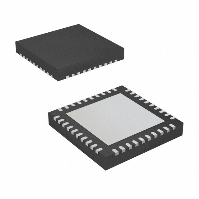
40-lead 6 mm × 6 mm LFCSP
The ADRF6720 is a wideband quadrature modulator with an
integrated synthesizer ideally suited for 3G and 4G
communication systems. The ADRF6720 consists of a high
linearity broadband modulator, an integrated fractional-N
phase-locked loop (PLL), and four low phase noise multicore
voltage controlled oscillators (VCOs).
The ADRF6720 local oscillator (LO) signal can be generated
internally via the on-chip integer-N and fractional-N
synthesizers, or externally via a high frequency, low phase noise
LO signal. The internal integrated synthesizer enables LO
coverage from 356.25 MHz to 2855 MHz using the multicore
VCOs. In the case of internal LO generation or external LO
input, quadrature signals are generated with a divide-by-2 phase
splitter. When the ADRF6720 is operated with an external 1 ×
LO input, a polyphase filter generates the quadrature inputs to
the mixer.
The ADRF6720 offers digital programmability for carrier
feedthrough optimization, sideband suppression, HD3/IP3
optimization, and high-side or low-side LO injection.
APPLICATIONS
2G/3G/4G/LTE broadband communication systems
Microwave point-to-point radios
Satellite modems
Military/aerospace
Instrumentation
The ADRF6720 is fabricated using an advanced silicongermanium BiCMOS process. It is available in a 40-lead,
RoHS-compliant, 6 mm × 6 mm LFCSP package with an
exposed pad. Performance is specified over the −40°C to +85°C
temperature range.
FUNCTIONAL BLOCK DIAGRAM
VPOSx
40
30
26
22
17
11
6
3
ADRF6720
V TO I
I–
4
LO NULLING
DAC
LO NULLING
DAC
Q–
8
27
ENBL
24
RFOUT
18
LOOUT+
19
LOOUT–
15
CS
14
SCLK
13
SDIO
PHASE
CORRECTION
PHASE
CORRECTION
V TO I
Q+
9
REFIN
39
CP
36
VTUNE
32
LOIN–
33
LOIN+
34
PLL
QUAD
DIVIDER
POLYPHASE
FILTER
2
5
7 10 16 20 23 25 29 37 38
LDO
2.5V
LDO
VCO
12
28
DECL1
DECL2
GND
SERIAL
PORT
INTERFACE
31
DECL3
12134-001
I+
35
Figure 1.
Rev. 0
Document Feedback
Information furnished by Analog Devices is believed to be accurate and reliable. However, no
responsibility is assumed by Analog Devices for its use, nor for any infringements of patents or other
rights of third parties that may result from its use. Specifications subject to change without notice. No
license is granted by implication or otherwise under any patent or patent rights of Analog Devices.
Trademarks and registered trademarks are the property of their respective owners.
One Technology Way, P.O. Box 9106, Norwood, MA 02062-9106, U.S.A.
Tel: 781.329.4700
©2014 Analog Devices, Inc. All rights reserved.
Technical Support
www.analog.com
�ADRF6720
Data Sheet
TABLE OF CONTENTS
Features .............................................................................................. 1
Baseband Inputs ......................................................................... 24
Applications ....................................................................................... 1
LO Input ...................................................................................... 24
General Description ......................................................................... 1
Loop Filter ................................................................................... 24
Revision History ............................................................................... 2
RF Output .................................................................................... 24
Specifications..................................................................................... 3
Applications Information .............................................................. 25
Timing Characteristics ................................................................ 7
DAC-to-I/Q Modulator Interfacing......................................... 25
Absolute Maximum Ratings ............................................................ 8
Baseband Bandwidth ................................................................. 25
Thermal Resistance ...................................................................... 8
Carrier Feedthrough Nulling .................................................... 26
ESD Caution .................................................................................. 8
Sideband Suppression Optimization ....................................... 26
Pin Configuration and Function Descriptions ............................. 9
Linearity ....................................................................................... 27
Typical Performance Characteristics ........................................... 11
LO Amplitude and Common Mode Voltage .......................... 27
Theory of Operation ...................................................................... 18
Layout ........................................................................................... 27
LO Generation Block.................................................................. 18
Characterization Setups ................................................................. 29
Baseband ...................................................................................... 21
Register Map ................................................................................... 31
Active Mixers .............................................................................. 21
Register Details ............................................................................... 32
Serial Port Interface .................................................................... 22
Outline Dimensions ....................................................................... 42
Basic Connections for Operation ................................................. 23
Ordering Guide .......................................................................... 42
Power Supply and Grounding ................................................... 23
REVISION HISTORY
4/14—Revision 0: Initial Version
Rev. 0 | Page 2 of 44
�Data Sheet
ADRF6720
SPECIFICATIONS
VPOSx = 3.3 V, TA = 25°C; baseband I/Q amplitude = 1 V p-p differential sine waves in quadrature with a 500 mV dc bias, unless
otherwise noted.
Table 1.
Parameter
OPERATING FREQUENCY
RANGE
RF OUTPUT = 940 MHz
Output Power, POUT
Modulator Voltage Gain
Output P1dB
Carrier Feedthrough
Sideband Suppression
Quadrature Error
I/Q Amplitude Balance
Second Harmonic
Third Harmonic
Output IP2
Output IP3
Noise Floor
RF OUTPUT = 1900 MHz
Output Power, POUT
Modulator Voltage Gain
Output P1dB
Carrier Feedthrough
Sideband Suppression
Quadrature Error
I/Q Amplitude Balance
Second Harmonic
Third Harmonic
Output IP2
Output IP3
Noise Floor
RF OUTPUT = 2140 MHz
Output Power, POUT
Modulator Voltage Gain
Output P1dB
Carrier Feedthrough
Sideband Suppression
Quadrature Error
I/Q Amplitude Balance
Second Harmonic
Third Harmonic
Test Conditions/Comments
RF output range
Min
700
Internal LO range
External LO range
356.25
700
Baseband VIQ = 1 V p-p differential
POUT − P(fLO ± (2 × fBB))
POUT − P(fLO ± (3 × fBB))
f1BB = 3.5 MHz, f2BB = 4.5 MHz, baseband I/Q amplitude per tone =
0.45 V p-p differential
f1BB = 3.5 MHz, f2BB = 4.5 MHz, baseband I/Q amplitude per tone =
0.45 V p-p differential
I/Q input with 500 mV dc bias and no RF output, 20 MHz carrier offset
I/Q input with 500 mV dc bias and −10 dBm RF output, 20 MHz carrier
offset
Baseband VIQ = 1 V p-p differential
POUT − P(fLO ± (2 × fBB))
POUT − P(fLO ± (3 × fBB))
Rev. 0 | Page 3 of 44
Typ
Max
3000
Unit
MHz
2855
3000
MHz
MHz
5.8
1.82
13.1
−44.0
−47.1
−0.15
−0.01
−66.1
−60.6
66.4
dBm
dB
dBm
dBm
dBc
Degrees
dB
dBc
dBc
dBm
36.2
dBm
−157.6
−157.3
dBm/Hz
dBm/Hz
5.6
1.62
13.1
−39.2
−41.2
1.15
−0.0175
−66.2
−57.2
62.2
dBm
dB
dBm
dBm
dBc
Degrees
dB
dBc
dBc
dBm
35.7
dBm
−158.8
−158.1
dBm/Hz
dBm/Hz
5
1.12
12.2
−40.3
−37.6
−1.15
−0.022
−57.9
−58.1
dBm
dB
dBm
dBm
dBc
Degrees
dB
dBc
dBc
�ADRF6720
Parameter
Output IP2
Output IP3
Noise Floor
RF OUTPUT = 2300 MHz
Output Power, POUT
Modulator Voltage
Gain
Output P1dB
Carrier Feedthrough
Sideband Suppression
Quadrature Error
I/Q Amplitude Balance
Second Harmonic
Third Harmonic
Output IP2
Output IP3
Noise Floor
RF OUTPUT = 2600 MHz
Output Power, POUT
Modulator Voltage
Gain
Output P1dB
Carrier Feedthrough
Sideband Suppression
Quadrature Error
I/Q Amplitude Balance
Second Harmonic
Third Harmonic
Output IP2
Output IP3
Noise Floor
SYNTHESIZER
SPECIFICATIONS
Figure of Merit (FOM)1
REFERENCE
CHARACTERISTICS
REFIN Input
Frequency
REFIN Input
Amplitude
Phase Detector
Frequency
Data Sheet
Test Conditions/Comments
f1BB = 3.5 MHz, f2BB = 4.5 MHz, baseband I/Q amplitude per tone =
0.45 V p-p differential
f1BB = 3.5 MHz, f2BB = 4.5 MHz, baseband I/Q amplitude per tone =
0.45 V p-p differential
I/Q input with 500 mV dc bias and no RF output, 20 MHz carrier offset
I/Q input with 500 mV dc bias and −10 dBm RF output, 20 MHz carrier
offset
Min
Baseband VIQ = 1 V p-p differential
POUT − P(fLO ± (2 × fBB))
POUT − P(fLO ± (3 × fBB))
f1BB = 3.5 MHz, f2BB = 4.5 MHz, baseband I/Q amplitude per tone =
0.45 V p-p differential
f1BB = 3.5 MHz, f2BB = 4.5 MHz, baseband I/Q amplitude per tone =
0.45 V p-p differential
I/Q input with 500 mV dc bias and no RF output, 20 MHz carrier offset
I/Q input with 500 mV dc bias and −10 dBm RF output, 20 MHz carrier
offset
Synthesizer specifications referenced to the modulator output
Typ
57.7
Max
Unit
dBm
32.6
dBm
−157.9
−156.3
dBm/Hz
dBm/Hz
4.6
0.62
dBm
dB
11.8
−37.6
−36.6
−1.5
−0.0285
−54.8
−56.6
57.6
dBm
dBm
dBc
Degrees
dB
dBc
dBc
dBm
30.4
dBm
−159.2
−157.5
dBm/Hz
dBm/Hz
3.9
−0.08
dBm
dB
11.3
−36.5
−42.3
−0.55
−0.021
−60.3
−54.7
56.6
dBm
dBm
dBc
Degrees
dB
dBc
dBc
dBm
29.9
dBm
−159.2
−157.3
dBm/Hz
dBm/Hz
−218.5
dBc/Hz/Hz
REFIN, MUXOUT pins
5.7
320
4
11.4
Rev. 0 | Page 4 of 44
MHz
dBm
40
MHz
�Data Sheet
Parameter
MUXOUT Output Level
MUXOUT Duty Cycle
CHARGE PUMP
Charge Pump Current
Output Compliance
Range
PHASE NOISE,
FREQUENCY =
940 MHz,
fPFD = 38.4 MHz
Integrated Phase
Noise
Reference Spurs
PHASE NOISE,
FREQUENCY =
1900 MHz,
fPFD = 38.4 MHz
Integrated Phase
Noise
Reference Spurs
PHASE NOISE,
FREQUENCY =
2140 MHz,
fPFD = 38.4 MHz
Integrated Phase
Noise
Reference Spurs
ADRF6720
Test Conditions/Comments
Low (lock detect output selected)
High (lock detect output selected)
Min
Programmable to 250 μA, 500 μA, 750 μA, or 1000 μA
Typ
0.25
2.7
50
Max
1000
1
2.8
Unit
V
V
%
μA
V
Closed-loop operation (20 kHz loop filter, see Figure 44 for loop filter
design)
10 kHz offset
100 kHz offset
1 MHz offset
5 MHz offset
10 MHz offset
20 MHz offset
1 kHz to 40 MHz integration bandwidth, with spurs
−97.8
−120.8
−144.4
−154.4
−154.9
−155.3
0.175
dBc/Hz
dBc/Hz
dBc/Hz
dBc/Hz
dBc/Hz
dBc/Hz
° rms
fPFD
fPFD × 2
fPFD × 3
fPFD × 4
Closed-loop operation (20 kHz loop filter, see Figure 44 for loop filter
design)
−104.8
−97.8
−98.8
−103
dBc
dBc
dBc
dBc
10 kHz offset
100 kHz offset
1 MHz offset
5 MHz offset
10 MHz offset
20 MHz offset
1 kHz to 40 MHz integration bandwidth, with spurs
−91.5
−114.5
−139.9
−151.4
−153
−153.5
0.332
dBc/Hz
dBc/Hz
dBc/Hz
dBc/Hz
dBc/Hz
dBc/Hz
° rms
fPFD
fPFD × 2
fPFD × 3
fPFD × 4
Closed-loop operation (20 kHz loop filter, see Figure 44 for loop filter
design)
−102
−90.8
−93.6
−100.5
dBc
dBc
dBc
dBc
10 kHz offset
100 kHz offset
1 MHz offset
5 MHz offset
10 MHz offset
20 MHz offset
1 kHz to 40 MHz integration bandwidth, with spurs
−92
−115.7
−140.3
−151.3
−152.1
−152.9
0.305
dBc/Hz
dBc/Hz
dBc/Hz
dBc/Hz
dBc/Hz
dBc/Hz
° rms
fPFD
fPFD × 2
fPFD × 3
fPFD × 4
−95.9
−93.1
−87.4
−91.5
dBc
dBc
dBc
dBc
Rev. 0 | Page 5 of 44
�ADRF6720
Parameter
PHASE NOISE,
FREQUENCY =
2300 MHz,
fPFD = 38.4 MHz
Integrated Phase
Noise
Reference Spurs
PHASE NOISE,
FREQUENCY =
2600 MHz,
fPFD = 38.4 MHz
Integrated Phase
Noise
Reference Spurs
LO INPUT/OUTPUT
LO Output Frequency
Range
LO Output Level
LO Input Level
LO Input Impedance
BASEBAND INPUTS
I and Q Input DC Bias
Level
Bandwidth
Differential Input
Impedance
Differential Input
Capacitance
OUT ENABLE
Turn-On Settling Time
Turn-Off Settling Time
Data Sheet
Test Conditions/Comments
Closed-loop operation (20 kHz loop filter, see Figure 44 for loop filter
design)
Min
Typ
Max
Unit
10 kHz offset
100 kHz offset
1 MHz offset
5 MHz offset
10 MHz offset
20 MHz offset
1 kHz to 40 MHz integration bandwidth, with spurs
−94.1
−114.6
−138.7
−150.1
−151.4
−152.6
0.270
dBc/Hz
dBc/Hz
dBc/Hz
dBc/Hz
dBc/Hz
dBc/Hz
° rms
fPFD
fPFD × 2
fPFD × 3
fPFD × 4
Closed-loop operation (20 kHz loop filter, see Figure 44 for loop filter
design)
−100.8
−95.6
−89.4
−93.1
dBc
dBc
dBc
dBc
10 kHz offset
100 kHz offset
1 MHz offset
5 MHz offset
10 MHz offset
20 MHz offset
1 kHz to 40 MHz integration bandwidth, with spurs
−91.5
−111.3
−136.8
−148.3
−150
−150.7
0.378
dBc/Hz
dBc/Hz
dBc/Hz
dBc/Hz
dBc/Hz
dBc/Hz
°rms
fPFD
fPFD × 2
fPFD × 3
fPFD × 4
−97.4
−89.3
−95.2
−91.4
dBc
dBc
dBc
dBc
LO output
700
2 × LO or 1 × LO mode, into a 50 Ω load, LO buffer enabled at 2140 MHz
LO_DRV_LVL = 0
LO_DRV_LVL = 1
LO_DRV_LVL = 2
Externally applied LO, PLL disabled
Externally applied LO, PLL disabled
I± and Q± pins
−6
2855
−5.1
−0.5
3
0
50
+6
MHz
dBm
dBm
dBm
dBm
Ω
0.5
V
1 dB
Frequency = 10 MHz2
>1000
465
MHz
Ω
Frequency = 10 MHz2
1.84
pF
190
ns
20
ns
ENBL pin
ENBL high to low (90% of envelope), when Register 0x01[10] = 1,
Register 0x10[10] = 1
ENBL low to high (10% of envelope), when Register 0x01[10] = 1,
Register 0x10[10] = 1
Rev. 0 | Page 6 of 44
�Data Sheet
ADRF6720
Parameter
DIGITAL LOGIC
Input Voltage High (VIH)
Input Voltage Low (VIL)
Input Current (IIH/IIL)
Input Capacitance
(CIN)
Output Voltage High
(VOH)
Output Voltage Low
(VOL)
POWER SUPPLIES
Voltage Range
Supply Current
Test Conditions/Comments
SCLK, SDIO, CS, and ENBL
Min
Typ
Max
Unit
0.7
1
V
V
µA
pF
1.4
−1
5
IOH = −100 uA
2.3
V
IOL = 100 uA
0.2
VPOSx
Tx mode at internal LO mode (PLL, internal VCO , and modulator
enabled, LO output driver disabled)
Tx mode at external 1× LO mode (PLL, internal VCO disabled,
modulator enabled, LO output driver disabled)
LO output driver; LO_DRV_LVL bits (Register 0x22[7:6]) = 10
Power-down mode
V
3.3
425
V
mA
228
mA
50
14.5
mA
mA
The figure of merit (FOM) is computed as phase noise (dBc/Hz) – 10log10(fPFD) − 20log10(fLO/fPFD). The FOM was measured across the full LO range, with fREF =
153.6 MHz, fREF power = 4 dBm with a 38.4 MHz fPFD. The FOM was computed at a 50 kHz offset.
2
Refer to Figure 47 for a plot of input impedance over frequency.
1
TIMING CHARACTERISTICS
Table 2.
Parameter
tSCLK
tDS
tDH
tS
tH
tHIGH
tLOW
tACCESS
tz
Description
Serial clock period
Setup time between data and rising edge of SCLK
Hold time between data and rising edge of SCLK
Setup time between falling edge of CS and SCLK
Hold time between rising edge of CS and SCLK
Minimum period that SCLK should be in a logic high state
Minimum period that SCLK should be in a logic low state
Maximum time delay between falling edge of SCLK and output data valid for a read operation
Maximum time delay between CS deactivation and SDIO bus return to high impedance
tHIGH
tDS
tS
Min
38
8
8
10
10
10
10
Max
231
5
Units
ns
ns
ns
ns
ns
ns
ns
ns
ns
tH
tSCLK
tACCESS
tLOW
tDH
Typ
CS
DON'T CARE
SDIO
DON'T CARE
DON'T CARE
tZ
A6
A5
A4
A3
A2
A1
A0
R/W
D15
D14
D13
Figure 2. Serial Port Timing Diagram
Rev. 0 | Page 7 of 44
D3
D2
D1
D0
DON'T CARE
12134-002
SCLK
�ADRF6720
Data Sheet
ABSOLUTE MAXIMUM RATINGS
THERMAL RESISTANCE
Table 3.
Parameter
Supply Voltage
I+, I−, Q+, Q−
LOIN+, LOIN−
REFIN
ENBL
VTUNE
CS, SCLK, SDIO
Maximum Junction Temperature
Operating Temperature Range
Storage Temperature Range
θJA is thermal resistance, junction to ambient (°C/W), and θJC is
thermal resistance, junction to case (°C/W).
Rating
−0.3 V to +3.6 V
−0.5 V to +1.5 V
16 dBm differential
−0.3 V to +3.6 V
−0.3 V to +3.6 V
−0.3 V to +3.6 V
−0.3 V to +3.6 V
150°C
−40°C to +85°C
−65°C to +150°C
Table 4. Thermal Resistance
Package Type
40-Lead LFCSP
1
θJA1
30.23
θJC1
0.44
Unit
°C/W
See JEDEC standard JESD51-2 for information on optimizing thermal
impedance.
ESD CAUTION
Stresses at or above those listed under Absolute Maximum
Ratings may cause permanent damage to the product. This is a
stress rating only; functional operation of the product at these
or any other conditions above those indicated in the operational
section of this specification is not implied. Operation beyond
the maximum operating conditions for extended periods may
affect product reliability.
Rev. 0 | Page 8 of 44
�Data Sheet
ADRF6720
40
39
38
37
36
35
34
33
32
31
VPOS8
REFIN
GND
GND
CP
VPOS7
LOIN+
LOIN–
VTUNE
DECL3
PIN CONFIGURATION AND FUNCTION DESCRIPTIONS
ADRF6720
TOP VIEW
(Not to Scale)
30
29
28
27
26
25
24
23
22
21
VPOS6
GND
DECL2
ENBL
VPOS5
GND
RFOUT
GND
VPOS4
NIC
NOTES
1. NIC = NOT INTERNALLY CONNECTED.
2. SOLDER THE EXPOSED PAD TO A LOW IMPEDANCE
GROUND PLANE.
12134-003
VPOS2
DECL1
SDIO
SCLK
CS
GND
VPOS3
LOOUT+
LOOUT–
GND
11
12
13
14
15
16
17
18
19
20
MUXOUT 1
GND 2
I+ 3
I– 4
GND 5
VPOS1 6
GND 7
Q– 8
Q+ 9
GND 10
Figure 3. Pin Configuration
Table 5. Pin Function Descriptions
Pin No.
1
Mnemonic
MUXOUT
2, 10
3, 4
5, 7
6
GND
I+, I−
GND
VPOS1
8, 9
11
Q−, Q+
VPOS2
12
DECL1
13
14
15
16
17
SDIO
SCLK
CS
GND
VPOS3
18, 19
LOOUT+, LOOUT−
20
21
22
GND
NIC
VPOS4
23, 25
24
26
GND
RFOUT
VPOS5
27
ENBL
28
DECL2
29
GND
Description
Multiplexer Output. This output allows a digital lock detect signal, a voltage
proportional to absolute temperature (VPTAT), or a buffered, frequency-scaled
reference signal to be accessed externally. The output is selected by programming
Bits[6:4] in Register 0x21.
Baseband Ground.
Differential In-Phase Baseband Inputs.
Mixer Core (I and Q) Ground.
3.3 V Supply Voltage for Baseband. Decouple VPOS1 with 100 pF and 0.1 µF
capacitors located close to the pin.
Differential Quadrature Baseband Inputs.
3.3 V Supply Voltage for 2.5 V LDO. Decouple VPOS2 with 100 pF and 0.1 µF
capacitors located close to the pin.
Decoupling Pin for 2.5 V LDO. Connect 100 pF, 0.1 µF, and 10 µF capacitors between
this pin and ground.
Serial Data Input/Output for SPI.
Serial Clock Input/Output for SPI.
Chip Select Input/Output for SPI.
Digital Ground.
3.3 V Supply Voltage for LO. Decouple VPOS3 with 100 pF and 0.1 µF capacitors
located close to the pin.
Differential LO Outputs. Either the internally generated LO or external 1 × LO/2 × LO
is available at 1 × LO or 2 × LO on these pins.
LO Ground.
Not Internally Connected. This pin can be left open or tied to RF ground.
3.3 V Supply Voltage for RF. Decouple VPOS4 with 100 pF and 0.1 µF capacitors
located close to the pin.
RF Ground.
Single-Ended 0 V DC RF Output.
3.3 V Supply Voltage for RF. Decouple VPOS5 with 100 pF and 0.1 µF capacitors
located close to the pin.
Enables/Disables the Circuit Blocks. References the settings at Register 0x01 and
Register 0x10. Refer to the ENBL section for more information.
Decoupling Pin for VCO LDO. Connect 100 pF, 0.1 µF, and 10 µF capacitors between
this pin and ground.
VCO Ground.
Rev. 0 | Page 9 of 44
�ADRF6720
Data Sheet
Pin No.
30
Mnemonic
VPOS6
31
DECL3
32
33, 34
35
VTUNE
LOIN−, LOIN+
VPOS7
36
37
38
39
40
CP
GND
GND
REFIN
VPOS8
EP
Description
3.3 V Supply Voltage for VCO LDO. Decouple VPOS6 with 100 pF and 0.1 µF
capacitors located close to the pin.
Decoupling Pin for VCO LDO. Connect 100 pF, 0.1 µF, and 10 µF capacitors between
this pin and ground.
VCO Tuning Voltage.
Differential External LO Inputs.
3.3 V Supply Voltage for Charge Pump. Decouple VPOS7 with 100 pF and 0.1 µF
capacitors located close to the pin.
Charge Pump Output.
Charge Pump Ground.
PLL Reference Ground.
PLL Reference Input.
3.3 V Supply Voltage for PLL Reference. Decouple VPOS8 with 100 pF and 0.1 µF
capacitors located close to the pin.
Exposed Pad. Solder the exposed pad to a low impedance ground plane.
Rev. 0 | Page 10 of 44
�Data Sheet
ADRF6720
TYPICAL PERFORMANCE CHARACTERISTICS
VPOSx = 3.3 V; TA = 25°C; baseband I/Q amplitude = 1 V p-p differential sine waves in quadrature with a 500 mV dc bias; baseband I/Q
frequency (fBB) = 1 MHz; fPFD = 38.4 MHz; fREF = 153.6 MHz at 4 dBm referred to 50 Ω (1 V p-p); 20 kHz loop filter, unless otherwise
noted.
9
9
SSB OUTPUT POWER (dBm)
8
7
6
5
4
3
5
4
3
1
1200
1700
2200
2700
0
700
16
1dB OUTPUT COMPRESSION (dBm)
10
8
6
4
2700
14
3.15V
3.3V
3.45V
12
10
8
6
4
1700
2200
2700
LO FREQUENCY (MHz)
0
700
12134-005
1200
2200
2700
Figure 8. SSB 1 dB Output Compression Point (OP1dB) vs. LO Frequency (fLO)
and Supply
0
TA = –40°C
TA = +25°C
TA = +85°C
–10
CARRIER FEEDTHROUGH (dBm)
–10
1700
LO FREQUENCY (MHz)
Figure 5. SSB 1 dB Output Compression Point (OP1dB) vs. LO Frequency (fLO)
and Temperature; Multiple Devices Shown
0
1200
12134-008
2
2
–20
–30
–40
–50
–60
–70
TA = –40°C
TA = +25°C
TA = +85°C
–20
–30
–40
–50
–60
–70
1700
2200
LO FREQUENCY (MHz)
2700
–90
700
12134-006
1200
1200
1700
2200
LO FREQUENCY (MHz)
Figure 6. Carrier Feedthrough vs. LO Frequency (fLO) and Temperature Before
Nulling; Multiple Devices Shown
2700
12134-009
–80
–80
–90
700
2200
16
12
0
700
1700
Figure 7. SSB Output Power (POUT) vs. LO Frequency (fLO) and Supply
TA = –40°C
TA = +25°C
TA = +85°C
14
1200
LO FREQUENCY (MHz)
Figure 4. Single Sideband (SSB) Output Power (POUT) vs. LO Frequency (fLO)
and Temperature; Multiple Devices Shown
1dB OUTPUT COMPRESSION (dBm)
6
1
LO FREQUENCY (MHz)
CARRIER FEEDTHROUGH (dBm)
7
2
0
700
3.15V
3.3V
3.45V
8
2
12134-004
SSB OUTPUT POWER (dBm)
10
TA = –40°C
TA = +25°C
TA = +85°C
12134-007
10
Figure 9. Carrier Feedthrough vs. LO Frequency (fLO) and Temperature After
Nulling Using DCOFF_I and DCOFF_Q at 25°C; Multiple Devices Shown
Rev. 0 | Page 11 of 44
�ADRF6720
Data Sheet
0
0
TA = –40°C
TA = +25°C
TA = +85°C
–20
–30
–40
–50
–60
–70
–30
–40
–50
–60
–70
LO FREQUENCY (MHz)
–90
700
OIP2
–20
TA = –40°C
TA = +25°C
TA = +85°C
60
50
40
30
OIP3
20
10
1200
1700
2200
2700
LO FEQUENCY (MHz)
10
–30
5
SIDEBAND
SUPPRESSION (dBc)
–40
0
–5
–50
–60
–10
CARRIER
FEEDTHROUGH (dBm)
SECOND-ORDER
HARMONIC (dBc)
–70
–80
0.1
1
SECOND-ORDER HARMONIC (dBc),
THIRD-ORDER HARMONIC (dBc),
CARRIER FEEDTHROUGH (dBm),
SIDEBAND SUPPRESSION (dBc)
SSB OUTPUT
POWER (dBm)
15
SSB OUTPUT POWER (dBm)
–20
–50
–60
–70
–80
1200
1700
2200
2700
0
–15
–20
10
BASEBAND INPUT VOLTAGE (V p-p Differential)
Figure 12. SSB Output Power, Second- and Third-Order Harmonics, Carrier
Feedthrough, and Sideband Suppression vs. Baseband Differential Input
Voltage (fOUT = 940 MHz)
20
THIRD-ORDER
HARMONIC (dBC)
–10
–20
–30
15
SSB OUTPUT
POWER (dBm)
10
SIDEBAND
SUPPRESSION (dBC)
5
–40
0
CARRIER
FEEDTHROUGH (dBm)
–50
–60
SECOND-ORDER
HARMONIC (dBC)
–80
0.1
–5
–10
–15
–70
12134-012
–10
–40
Figure 14. Second- and Third-Order Harmonics vs. LO Frequency (fLO) and
Temperature (POUT ≈ 5 dBm)
20
THIRD-ORDER
HARMONIC (dBc)
–30
SECOND-ORDER
THIRD-ORDER
LO FREQUENCY (MHz)
Figure 11. OIP3 and OIP2 vs. LO Frequency (fLO) and Temperature (POUT ≈
−5 dBm per Tone); Multiple Devices Shown
0
TA = –40°C
TA = +25°C
TA = +85°C
–90
700
12134-011
0
700
2700
2200
Figure 13. Sideband Suppression vs. LO Frequency (fLO) and Temperature
After Nulling Using I_LO and Q_LO at 25°C; Multiple Devices Shown
THIRD-ORDER HARMONIC (dBc),
SECOND-ORDER HARMONIC (dBc)
70
1700
LO FREQUENCY (MHz)
Figure 10. Sideband Suppression vs. LO Frequency (fLO) and Temperature
Before Nulling; Multiple Devices Shown
80
1200
SSB OUTPUT POWER (dBm)
2700
1
–20
10
BASEBAND INPUT VOLTAGE (V p-p Differential)
Figure 15. SSB Output Power, Second- and Third-Order Harmonics, Carrier
Feedthrough, and Sideband Suppression vs. Baseband Differential Input
Voltage (fOUT = 2140 MHz)
Rev. 0 | Page 12 of 44
12134-015
2200
12134-013
1700
12134-014
1200
12134-010
–90
700
OUTPUT IP3 AND IP2 (dBm)
–20
–80
–80
SECOND-ORDER HARMONIC (dBc),
THIRD-ORDER HARMONIC (dBc),
CARRIER FEEDTHROUGH (dBm),
SIDEBAND SUPPRESSION (dBc)
TA = –40°C
TA = +25°C
TA = +85°C
–10
SIDEBAND SUPPRESSION (dBc)
SIDEBAND SUPPRESSION (dBc)
–10
�Data Sheet
ADRF6720
0
15
–20
–20
5
–40
0
–50
–5
SECOND-ORDER
HARMONIC (dBC)
–60
SIDEBAND
SUPPRESSION (dBC)
–70
–80
0.1
1
–10
–120
–20
10
–180
10M
TA = –40°C
TA = +25°C
TA = +85°C
–40
–60
–80
–100
–120
–140
–140
–160
–160
10k
100k
1M
10M
OFFSET FREQUENCY (Hz)
–180
1k
1M
10M
Figure 20. Closed-Loop Phase Noise vs. Offset Frequency and Temperature,
fLO = 2140 MHz; 20 kHz Loop Filter
0
TA = –40°C
TA = +25°C
TA = +85°C
–20
100k
OFFSET FREQUENCY (Hz)
Figure 17. Closed-Loop Phase Noise vs. Offset Frequency and Temperature,
fLO = 1900 MHz; 20 kHz Loop Filter
0
10k
12134-020
PHASE NOISE (dBc/Hz)
–120
TA = –40°C
TA = +25°C
TA = +85°C
–20
–40
PHASE NOISE (dBc/Hz)
–40
–60
–80
–100
–120
–60
–80
–100
–120
–140
–140
–160
–160
10k
100k
1M
OFFSET FREQUENCY (Hz)
10M
–180
12134-018
1k
1M
–20
–100
–180
100k
0
–80
1k
10k
Figure 19. Closed-Loop Phase Noise vs. Offset Frequency and Temperature,
fLO = 940 MHz; 20 kHz Loop Filter
TA = –40°C
TA = +25°C
TA = +85°C
–60
–180
1k
OFFSET FREQUENCY (Hz)
12134-017
PHASE NOISE (dBc/Hz)
–100
–140
–40
PHASE NOISE (dBc/Hz)
–80
–160
Figure 16. SSB Output Power, Second- and Third-Order Harmonics, Carrier
Feedthrough, and Sideband Suppression vs. Baseband Differential Input
Voltage (fOUT = 2600 MHz)
–20
–60
–15
BASEBAND INPUT VOLTAGE (V p-p Differential)
0
–40
Figure 18. Closed-Loop Phase Noise vs. Offset Frequency and Temperature,
fLO = 2300 MHz; 20 kHz Loop Filter
1k
10k
100k
1M
OFFSET FREQUENCY (Hz)
10M
12134-021
–30
10
CARRIER
FEEDTHROUGH (dBm)
TA = –40°C
TA = +25°C
TA = +85°C
12134-019
SSB OUTPUT
POWER (dBm)
PHASE NOISE (dBc/Hz)
–10
20
SSB OUTPUT POWER (dBm)
THIRD-ORDER
HARMONIC (dBC)
12134-016
SECOND-ORDER HARMONIC (dBc),
THIRD-ORDER HARMONIC (dBc),
CARRIER FEEDTHROUGH (dBm),
SIDEBAND SUPPRESSION (dBc)
0
Figure 21. Closed-Loop Phase Noise vs. Offset Frequency and Temperature,
fLO = 2600 MHz; 20 kHz Loop Filter
Rev. 0 | Page 13 of 44
�ADRF6720
OFFSET = 1kHz
–90
–130
–140
OFFSET = 5MHz
–120
–130
OFFSET = 1MHz
–140
–150
–150
–160
–160
1200
1700
2200
2700
LO FREQUENCY (MHz)
Figure 22. Closed-Loop Phase Noise vs. LO Frequency at 1 kHz, 100 kHz, and
5 MHz Offsets
1 × PFD FREQUENCY
3 × PFD FREQUENCY
–170
700
–85
SPUR LEVEL (dBc)
–85
–90
–95
–100
–105
–95
–100
–105
–110
–115
–115
–120
700
–120
700
2700
–75
2 × PFD FREQUENCY
4 × PFD FREQUENCY
–85
SPUR LEVEL (dBc)
–80
–90
–95
–100
–105
–95
–100
–105
–115
–115
–120
700
–120
700
12134-024
–110
2700
2700
–90
–110
2200
2200
–75
–85
1700
1700
–70
TA = –40°C
TA = +25°C
TA = +85°C
LO FREQUENCY (MHz)
1200
1 × PFD FREQUENCY
3 × PFD FREQUENCY
Figure 26. PLL Reference Spurs vs. LO Frequency (1 × PFD and 3 × PFD) at LO
Output
–80
1200
TA = –40°C
TA = +25°C
TA = +85°C
LO FREQUENCY (MHz)
Figure 23. PLL Reference Spurs vs. LO Frequency (1 × PFD and 3 × PFD) at
Modulator Output
–70
2700
–90
–110
2200
2200
–75
–80
1700
1700
–70
TA = –40°C
TA = +25°C
TA = +85°C
LO FREQUENCY (MHz)
1200
Figure 25. Closed-Loop Phase Noise vs. LO Frequency at 10 kHz, 1 MHz, and
10 MHz Offsets
–80
1200
OFFSET = 10MHz
LO FREQUENCY (MHz)
12134-023
SPUR LEVEL (dBc)
–75
SPUR LEVEL (dBc)
–110
12134-025
PHASE NOISE (dBc/Hz)
–120
12134-022
PHASE NOISE (dBc/Hz)
OFFSET = 100kHz
–110
–70
OFFSET = 10kHz
–100
–100
–170
700
TA = –40°C
TA = +25°C
TA = +85°C
12134-026
–90
–80
TA = –40°C
TA = +25°C
TA = +85°C
Figure 24. PLL Reference Spurs vs. LO Frequency (2 × PFD and 4 × PFD) at
Modulator Output
TA = –40°C
TA = +25°C
TA = +85°C
1200
2 × PFD FREQUENCY
4 × PFD FREQUENCY
1700
2200
LO FREQUENCY (MHz)
2700
12134-027
–80
Data Sheet
Figure 27. PLL Reference Spurs vs. LO Frequency (2 × PFD and 4 × PFD) at LO
Output
Rev. 0 | Page 14 of 44
�Data Sheet
ADRF6720
0.8
2.4
0.7
2.2
VTUNE (V)
0.6
0.5
0.4
2
1.8
1.6
0.3
1.4
0.2
1.2
0.1
1.0
0
700
1200
TA = –40°C
TA = +25°C
TA = +85°C
2.6
1700
2200
2700
LO FREQUENCY (MHz)
0.8
2800
12134-028
PHASE NOISE (dBc/Hz)
5800
2300.78MHz
2156.06MHz
2009.22MHz
–80
–100
–120
–140
10k
100k
1M
10M
100M
FREQUENCY (Hz)
–160
12134-029
1k
Figure 29. Open-Loop VCO Phase Noise for VCO 0 Measured at 2300.22 MHz,
2579.83 MHz, and 2860.8 MHz (VCO ÷ 2)
1k
10k
100k
1M
100M
Figure 32. Open-Loop VCO Phase Noise for VCO 1 Measured at 2009.22 MHz,
2156.06 MHz, and 2300.78 MHz (VCO ÷ 2)
–40
–40
10M
FREQUENCY (Hz)
12134-032
PHASE NOISE (dBc/Hz)
–120
–140
1751.47MHz
1587.28MHz
1425.29MHz
2010.75MHz
1882.97MHz
1750.48MHz
–60
PHASE NOISE (dBc/Hz)
–60
PHASE NOISE (dBc/Hz)
5300
–60
–100
–80
–100
–120
–80
–100
–120
–140
–140
1k
10k
100k
1M
FREQUENCY (Hz)
10M
100M
–160
12134-030
–160
4800
–40
–80
–160
4300
Figure 31. VTUNE vs. VCO Frequency and Temperature
2860.8MHz
2579.83MHz
2300.22MHz
–60
3800
VCO FREQUENCY (MHz)
Figure 28. Integrated Phase Noise with Spurs vs. LO Frequency and
Temperature
–40
3300
Figure 30. Open-Loop VCO Phase Noise for VCO 2 Measured at 1750.48 MHz,
1882.97 MHz, and 2010.75 MHz (VCO ÷ 2)
1k
10k
100k
1M
FREQUENCY (Hz)
10M
100M
12134-033
INTEGRATED PHASE NOISE (°rms)
0.9
2.8
TA = –40°C
TA = +25°C
TA = +85°C
12134-031
1.0
Figure 33. Open-Loop VCO Phase Noise for VCO 3 Measured at 1425.29 MHz,
1587.28 MHz, and 1751.47 MHz (VCO ÷ 2)
Rev. 0 | Page 15 of 44
�ADRF6720
Data Sheet
100
80
TA = –40°C
TA = +25°C
TA = +85°C
4
3
LO OUTPUT POWER (dBm)
90
CUMULATIVE PERCENTAGE (%)
5
940MHz
1900MHz
2140MHz
2300MHz
2600MHz
70
60
50
40
30
20
2
1
LO_DRV_LVL = 2
LO_DRV_LVL = 1
0
–1
–2
–3
LO_DRV_LVL = 0
–4
–5
–6
10
12134-034
NOISE FLOOR (dBm/Hz)
–8
700
Figure 34. Noise Floor Cumulative Distribution at Various LO Frequencies
Using Internal LO; I/Q Input with 500 mV DC Bias and No RF Output
520
500
2700
TA = –40°C
TA = +25°C
TA = +85°C
60
50
40
30
460
440
420
400
380
20
360
10
340
0
–163 –162 –161 –160 –159 –158 –157 –156 –155 –154 –153
NOISE FLOOR (dBm/Hz)
320
700
Figure 35. Noise Floor Cumulative Distribution at Various LO Frequencies
Using Internal LO; I/Q Input with 500 mV DC Bias and RF Output = −10 dBm
1200
1700
2200
2700
LO FREQUENCY (MHz)
12134-039
SUPPLY CURRENT (mA)
480
70
12134-035
CUMULATIVE PERCENTAGE (%)
2200
Figure 37. LO Output Power vs. LO Frequency at Various LO_DRV_LVL
Settings
940MHz
1900MHz
2140MHz
2300MHz
2600MHz
80
1700
LO FREQUENCY (MHz)
100
90
1200
12134-037
–7
0
–163 –162 –161 –160 –159 –158 –157 –156 –155 –154 –153
Figure 38. Supply Current vs. LO Frequency and Temperature (PLL and
I/Q Modulator Enabled, LO Buffer Disabled)
20
0
–5
10
5
0
–5
–10
–15
–20
–10
–25
–15
0
0.5
1.0
1.5
2.0
2.5
3.0
TIME (ms)
3.5
4.0
4.5
5.0
–30
0.7
12134-036
–20
Figure 36. Frequency Deviation from LO Frequency at LO = 1.91 GHz to
1.9 GHz vs. Lock Time
BAL_CIN = 0, BAL_COUT = 0
BAL_CIN = 1, BAL_COUT = 0
BAL_CIN = 2, BAL_COUT = 0
BAL_CIN = 3, BAL_COUT = 0
BAL_CIN = 4, BAL_COUT = 0
BAL_CIN = 8, BAL_COUT = 0
BAL_CIN = 9, BAL_COUT = 0
BAL_CIN = 10, BAL_COUT = 0
BAL_CIN = 11, BAL_COUT = 0
BAL_CIN = 12, BAL_COUT = 0
BAL_CIN = 13, BAL_COUT = 0
BAL_CIN = 14, BAL_COUT = 0
BAL_CIN = 15, BAL_COUT = 0
BAL_CIN = 15, BAL_COUT = 3
1.2
1.7
2.2
LO FREQUENCY (GHz)
2.7
12134-040
RETURN LOSS (dB)
FREQUENCY DEVIATION (MHz)
15
Figure 39. RF Output Return Loss vs. LO Frequency (fLO) for Multiple BAL_CIN
and BAL_COUT Combinations
Rev. 0 | Page 16 of 44
�Data Sheet
ADRF6720
0
0
–2
–5
RETURN LOSS (dB)
–6
–8
–10
–12
–14
–10
–15
–20
–25
–16
–30
–20
0.3
1.3
2.3
3.3
4.3
5.3
LO FREQUENCY (GHz)
6.3
Figure 40. LO Input Return Loss vs. LO Frequency (fLO)
–35
0.3
1.3
2.3
3.3
4.3
5.3
LO FREQUENCY (GHz)
Figure 41. LO Output Return Loss vs. LO Frequency (fLO)
Rev. 0 | Page 17 of 44
6.3
12134-042
–18
12134-041
RETURN LOSS (dB)
–4
�ADRF6720
Data Sheet
THEORY OF OPERATION
Internal LO Mode
The ADRF6720 integrates a high performance broadband I/Q
modulator with a fractional-N PLL and low noise multicore
VCOs. The baseband inputs mix with the LO generated
internally or provided externally, and convert it to a singleended RF using an integrated RF balun. A block diagram of the
device is shown in Figure 1. The ADRF6720 is programmed via
an SPI.
For internal LO mode, the ADRF6720 uses the on-chip PLL and
VCO to synthesize the frequency of the LO signal. The PLL,
shown in Figure 42, consists of a reference path, phase and
frequency detector (PFD), charge pump, and a programmable
integer divider with prescaler. The reference path takes in a
reference clock and divides it down by a factor of 2, 4, or 8, or
multiplies it by a factor of 1 or 2, and then passes it to the PFD.
The PFD compares this signal to the divided down signal from
the VCO. Depending on the PFD polarity selected, the PFD
sends either an up or down signal to the charge pump if the
VCO signal is either slow or fast compared to the reference
frequency. The charge pump sends a current pulse to the offchip loop filter to increase or decrease the tuning voltage
(VTUNE).
LO GENERATION BLOCK
The ADRF6720 supports the use of both internal and external
LO signals for the mixers. The internal LO is generated by an
on-chip VCO, which is tunable over an octave frequency range
of 2850 MHz to 5710 MHz. The output of the VCO is phaselocked to an external reference clock through a fractional-N
PLL that is programmable through the SPI control registers. To
produce in-phase and quadrature phase LO signals over the
356.25 MHz to 2855 MHz frequency range to drive the mixers,
steer the VCO outputs through a combination of frequency
dividers, as shown in Figure 42.
The ADRF6720 integrates four VCO cores, covering an octave
range of 2850 MHz to 5710 MHz.
Table 6 lists the frequency range covered by each VCO. The
desired VCO can be selected by addressing the VCO_SEL bits at
Register 0x22[2:0].
Alternatively, an external signal can be used with the dividers or
a polyphase phase splitter to generate the LO signals in
quadrature to the mixers. In demanding applications that
require the lowest possible phase noise performance, it may be
necessary to source the LO signal externally. The different
methods of quadrature LO generation and the control register
programming needed are listed in Table 6.
The LO source and quadrature generation path can be selected
by setting the QUAD_DIV_EN bit (Register 0x01[9]) and the
LO_1XVCO_EN bit (Register 0x01[11]). The mode of the VCO
signal through a polyphase filter is intended to extend the
operating frequency with an internal VCO and is only useful for
baseband input frequencies high enough to prevent the RF
output from pulling the VCO.
POLYPHASE
FILTER
LOIN+ 34
REF_SEL
REG 0x21[2:0]
÷4
PFD
÷2
+
×1
QUAD_DIV_EN
REG 0x01[9]
÷1, ÷2,
÷4
QUAD
DIVIDER
VTUNE
CP
CHARGE
PUMP
32
36
I+
I–
TO MIXER
Q+
Q–
LPF
CP_CTL
REG 0x20[14:0]
×2
LO_1XVCO_EN
REG 0x01[11]
EXTERNAL
LOOP
FILTER
PFD_POLARITY
REG 0x21[3]
÷8
REFIN 39
LOIN– 33
DIV8 _EN/
DIV4_EN
REG 0x22[4:3]
N = INT +
FRAC
MOD
÷1,÷2
÷2
DRVDIV2_EN
REG 0x22[5]
LOOUT+
LOOUT–
MUXOUT 1
VPTAT
DIV_MODE: REG 0x02[11]
INT_DIV: REG 0x02[10:0]
FRAC_DIV: REG 0x03[15:0]
MOD_DIV: REG 0x04[15:0]
REF_MUX_SEL
REG 0x21[6:4]
Figure 42. LO Block Diagram
Rev. 0 | Page 18 of 44
VCO_SEL
REG 0x22[2:0]
LO_DRV2X_EN REG 0x01[8]
LO_DRV1X_EN REG 0x01[7]
12134-043
LOCK_DET
�Data Sheet
ADRF6720
Table 6. LO Mode Selection
LO Selection
Internal (VCO)
External
1
fVCO or fEXT (MHz)
2850 to 3500
3500 to 4020
4020 to 4600
4600 to 5710
2855 to 3000
700 to 6000
700 to 3000
Quadrature
Generation
Divide by 2
Divide by 2
Divide by 2
Divide by 2
Polyphase
Divide by 2
Polyphase
QUAD_DIV_EN
(Register
0x01[9])
1
1
1
1
0
1
0
LO_1XVCO_EN
(Register
0x1 [11])
0
0
0
0
0
0
0
Enables
(Register
0x01[6:0])
111 111X1
111 111X1
111 111X1
111 111X1
111 111X1
101 000X1
000 000X1
VCO_SEL
(Register
0x22[2:0])
011
010
001
000
011
1XX1
XXX1
X = don’t care.
LO Frequency and Dividers
The signal coming from the VCO or the external LO inputs
goes through a series of dividers before it is buffered to drive
the active mixers. Two programmable divide-by-2 stages divide
the frequency of the incoming signal by 1, 2, or 4 before
reaching the quadrature divider that further divides the signal
frequency by 2 to generate the in-phase and quadrature phase
LO signals for the mixers. The control bits (Register 0x22[4:3])
needed to select the different LO frequency ranges are listed in
Table 7.
Table 7. LO Frequency and Dividers
LO Frequency
Range (MHz)
1425 to 2855
712.5 to 1425
356.25 to 712.5
fVCO/fLO or
fEXT LO/fLO
2
4
8
DIV8_EN
(Register
0x22[4])
0
0
1
DIV4_EN
(Register
0x22[3])
0
1
1
The N divider with divide-by-2 divides down the VCO signal to
the PFD frequency. The N divider can be configured for
fractional or integer mode by addressing the DIV_MODE bit
(Register 0x02[11]). The default configuration is set for
fractional mode. Use the following equations to determine the
N value and PLL frequency:
f VCO
2× N
The loop filter is connected between the CP and VTUNE pins.
The recommended components for 20 kHz filter designs are
shown in Table 8 and referenced in Figure 44.
The ADRF6720 closed-loop phase noise is characterized using a
20 kHz loop filter. Operation with an external VCO is possible.
In this case, the output of the loop filter is connected to the
tuning pin of the external VCO. The output of the VCO is
brought back into the device on the LOIN+ and LOIN− pins.
For assistance in designing loop filters with other characteristics,
download the most recent revision of ADIsimPLL™ from
http://www.analog.com/adisimpll.
Component
C57
R12
C58
R23
C59
R26
C60
20 kHz Loop Filter
2700 pF
300 Ω
100 nF
5.6 Ω
2700 pF
820 Ω
1500 pF
PLL Lock Time
FRAC
N = INT +
MOD
f LO =
Loop Filter
Table 8. Recommended Loop Filter Components
PLL Frequency Programming
f PFD =
locked.
LO_DIVIDER is the final frequency divider ratio that divides
the frequency of the VCO or the external LO signal down by 2,
4, or 8 before it reaches the mixer, as shown in Table 7.
It takes time to lock the PLL after the last register is written.
VCO band calibration time and loop settling time are used to
determine the PLL lock time.
f
×2× N
fvco
= PFD
LO _ DIVIDER LO_DIVIDER
where:
fPFD is the phase frequency detector frequency.
fVCO is the VCO frequency.
N is the fractional divide ratio (INT + FRAC/MOD).
INT is the integer divide ratio programmed in Register 0x02.
FRAC is the fractional divider programmed in Register 0x03.
MOD is the modulus divide ratio programmed in Register 0x04.
fLO is the LO frequency going to the mixer core when the loop is
After writing to the last register, the PLL automatically performs
a VCO band calibration to choose the correct VCO band. This
calibration takes approximately 94,208 PFD cycles. For a
40 MHz fPFD, this corresponds to 2.36 ms. After a band
calibration completes, the feedback action of the PLL results in
the VCO locking to the correct frequency. The speed to be
locked depends on the nonlinear cycle slipping behavior, as well
as the small signal settling of the loop. For an accurate
estimation of the lock time, download the ADIsimPLL tool to
Rev. 0 | Page 19 of 44
�ADRF6720
Data Sheet
capture these effects correctly. In general, higher bandwidth
loops tend to lock more quickly than lower bandwidth loops.
(fRF < fLO) when Q leads I and places the RF frequency above the
LO (fRF > fLO) when I leads Q.
The lock detect signal is available as one of the selectable
outputs through the MUXOUT pin, with a logic high signifying
that the loop is locked. The control bits for the MUXOUT pin
are the REF_MUX_SEL bits (Register 0x21[6:4]), and the
default configuration is for PLL lock detect.
Table 10. LO Polarity Setting
Address
0x32[11:10]
Bit
Name
POL_Q
01
Required PLL/VCO Settings and Register Write Sequence
In addition to writing to the necessary registers to configure the
PLL and VCO for the desired LO frequency and phase noise
performance, the registers listed in Table 9 are the required
registers to write.
To ensure that the PLL locks to the desired frequency, follow the
proper write sequence of the PLL registers. Configure the PLL
registers accordingly to achieve the desired frequency, and the
last writes must be to Register 0x02 (INT_DIV), Register 0x03
(FRAC_DIV), or Register 0x04 (MOD_DIV). When Register 0x02,
Register 0x03, and Register 0x04 are programmed, an internal
VCO calibration initiates, which is the last step to locking the
PLL.
Table 9. Required PLL/VCO Register Writes
Address
0x21[3]
0x49[13:0]
Bit Name
PFD_POLARITY
SET_1[13:9],
SET_0[8:0]
Setting
0x01
0x14B4
Description
Negative polarity
Internal settings
External LO Mode
Use the VCO_SEL bits (Register 0x22[2:0]) to select external or
internal LO mode. To configure for external LO mode, set
Register 0x22[2:0] to 4 decimal and apply the differential LO
signals to Pin 33 (LOIN−) and Pin 34 (LOIN+). The external
LO frequency range is 700 MHz to 3 GHz. When the polyphase
phase splitter is selected, a 1 × LO signal is required for the
active mixer, or a 2 × LO can be used with the internal
quadrature divider, as shown in Table 6.
There is also the option of using an external VCO with the
internal PLL. In this case, the PLL is enabled, but the VCO
blocks are turned off.
The LOIN+ and LOIN− input pins must be ac-coupled. When
not in use, leave the LOIN+ and LOIN− pins unconnected.
LO Polarity
The ADRF6720 offers the flexibility of specifying the
quadrature polarity on LO to the I channel or Q channel
mixers. This specification determines whether the LO is
injected above or below the RF frequency. RF frequency can
place either above or below the LO depending on the
Register 0x32[11:8] setting as well as the phase relationship
between the baseband I and Q. For normal operation and
characterization, the Register 0x32 settings are 2 decimal for POL_I
(Register 0x32[9:8]) and 1 decimal for POL_Q (Register 0x32,
Bits[11:10]). Setting Register 0x32 as such places the RF
frequency below the LO
Settings
10
0x32[9:8]
POL_I
01
10
Description
Quadrature polarity
switch, Q channel
Inverted Q channel
polarity
Normal polarity
Quadrature polarity
switch, I channel.
Normal polarity
Inverted I channel
polarity
LO Outputs
The ADRF6720 can provide either a differential 1 × or 2 × LO
output signal at the LOOUT+ and LOOUT− pins (Pin 18 and
Pin 19, respectively). The availability of the LO signal makes it
possible to daisy-chain many devices. One ADRF6720 device
can serve as the master where the LO signal is sourced, and the
subsequent slave devices can share the same LO output signal
from the master.
When the quadrature LO signals are generated using the
quadrature divider, the output signal is available at either 2× or
1× the frequency of the LO signal at the mixer by setting
LO_DRV2X_EN bit(Register 0x1[8]) and DRVDIV2_EN bit
(Register 0x22[5]). However, 1× the frequency of the LO signal
in this case has a phase ambiguity of 180° relative to the LO
signal that drives the mixer core. Because of this phase
ambiguity, the utility of this 1 × LO output signal as a system
daisy-chained LO signal is compromised. To avoid this
ambiguity, a second 1× the frequency of the LO signal output is
made available after the quadrature divider. This second 1 × LO
output path is enabled by setting the LO_DRV1X_EN bit
(Register 0x01[7]) high.
When the quadrature LO signals are generated using the
polyphase phase splitter, the output signal is also available at 1×
the frequency of the LO signal by setting LO_DRV1X_EN bit
(Register 0x10[7]) high.
Set the output to different drive levels by accessing the
LO_DRV_LVL bits (Register 0x22[7:6]), as shown in Table 11.
Table 11. LO Output Level at 2140 MHz
LO_DRV_LVL (Register 0x22[7:6])
00
01
10
Rev. 0 | Page 20 of 44
Amplitude (dBm)
−5.1
−0.5
3
�Data Sheet
ADRF6720
BASEBAND
Table 12. Optimum Balun Setting For Desired Frequency Range
The input impedance of the baseband inputs is a 500 Ω
differential. These inputs are designed to work with a 0.5 V
common-mode voltage. To match the 100 Ω impedance of the
DAC, place a shunt 125 Ω external resistor across the I and Q
inputs.
BAL_CIN
0
1
2
3
4
8
9
10
11
12
13
14
15
15
The voltages applied to the differential baseband inputs (I+, I−,
Q+, and Q−) drive the V-to-I stage that converts baseband
voltages into currents. The converted modulated signal current
feeds the modulator mixer core.
A programmable dc current can be added to both the I and Q
channels to null any carrier feedthrough at the RF output. Refer
to the Carrier Feedthrough Nulling section for more
information
The linearity can be optimized by adding the amplitude and
phase correction signals to the current output via the MOD_RSEL
(Register 0x31[12:6]) and MOD_CSEL (Register 0x31[5:0])
adjustment. Refer to the Linearity section for more information.
ACTIVE MIXERS
The ADRF6720 has two double balanced mixers: one for the
in-phase channel (I channel) and the other for the quadrature
channel (Q channel). They upconvert the modulated baseband
signal currents by the LO signals to the RF.
Tunable RFOUT Balun
The ADRF6720 integrates a programmable balun operating
over a frequency range from 700 MHz to 3000 MHz. It offers
single-ended-to-differential conversion and provides additional
common-mode noise rejection.
The capacitors at the input and output of the balun in parallel
with the inductive windings of the balun change the resonant
frequency of the inductor capacitor (LC) tank. Therefore,
selecting the proper combination of BAL_CIN (Register 0x30[3:0])
and BAL_COUT (Register 0x30[7:4]) sets the desired frequency
and optimizes gain. Under most circumstances, it is suggested to
set BAL_CIN and BAL_COUT over the frequency profile given
in Table 12. However, for matching reasons, it is advantageous to
tune the registers independently.
BAL_CIN
REG 0x30[3:0]
Figure 43. Integrated Tunable Balun
12134-044
RFOUT
BAL_COUT
REG 0x30[7:4]
BAL_COUT
0
0
0
0
0
0
0
0
0
0
0
0
0
3
Frequency Range (MHz)
fRF > 1730
1550 < fRF < 1730
1380 < fRF < 1550
1250 < fRF < 1380
1170 < fRF < 1250
1100 < fRF < 1170
1020 < fRF < 1100
970 < fRF < 1020
930 < fRF < 970
890 < fRF < 930
840 < fRF < 890
820 < fRF < 840
740 < fRF < 820
680 < fRF < 740
ENBL
The ENBL pin quickly enables/disables the RF output. The
circuit blocks that are enabled/disabled with the ENBL pin can
be programmed by setting the appropriate bits in the enables
register (Register 0x01) and the ENBL_MASK register
(Register 0x10). When the bits in the enables and the
ENBL_MASK register are 1, pulling the ENBL pin low disables
and pulling high enables the internal blocks more quickly than
possible with an SPI write operation.
Table 13. Enable/Disable Settings
Register
0x01
Enables
Bit1
0
Register 0x10
ENBL_MASK
Bit1
X2
ENBL Pin
Voltage
X2
1
0
X2
1
1
>1.8 V
1
1