700 MHz to 1050 MHz Quadrature
Demodulator with Fractional-N PLL
ADRF6807
Data Sheet
FEATURES
GENERAL DESCRIPTION
IQ demodulator with integrated fractional-N PLL
LO frequency range: 700 MHz to 1050 MHz
For the following specifications (LPEN = 0)/(LPEN = 1):
Input P1dB: 12.8 dBm/11.7 dBm
Input IP3: 26.7 dBm/24.0 dBm
Noise figure (DSB): 13.1 dB/12.4 dB
Voltage conversion gain: 1.0 dB/4.3 dB
Quadrature demodulation accuracy
Phase accuracy: 65
26.7
24.0
13.1
12.4
16
−73
dB
dBm
dBm
dBm
dBm
dBm
dBm
dB
dB
dB
dBm
1
dB
4.3
dB
170
135
0.35
0.05
±8
1.65
25
0.2
3
2.4
6
MHz
MHz
Degrees
dB
mV
V
mV
dB p-p
V p-p
V p-p
mA p-p
1.75
1
dBm
−0.75
dBm
0
50
4
dBm
Ω
4
8
2800
4200
MHz
�ADRF6807
Parameter
SYNTHESIZER SPECIFICATIONS
Channel Spacing
PLL Bandwidth
SPURS
Reference Spurs
PHASE NOISE (USING 67 kHz LOOP
FILTER)
Integrated Phase Noise
Phase Detector Frequency
PHASE NOISE (USING 2.5 kHz
LOOP FILTER)
PLL FIGURE OF MERIT (FOM)
Phase Detector Frequency
REFERENCE CHARACTERISTICS
REFIN Input Frequency
REFIN Input Capacitance
MUXOUT Output Level
REFOUT Duty Cycle
CHARGE PUMP
Pump Current
Output Compliance Range
LOGIC INPUTS
Input High Voltage, VINH
Input Low Voltage, VINL
Input Current, IINH/IINL
Input Capacitance, CIN
Data Sheet
Test Conditions/Comments
All synthesizer specifications measured with recommended
settings provided in Figure 33 through Figure 40
fPFD = 26 MHz
Can be adjusted with off-chip loop filter component values
and RSET
fLO = 900 MHz, fREF = 26 MHz, fPFD = 26 MHz, measured at
baseband outputs with fBB = 50 MHz
fREF = 26 MHz, fPFD = 26 MHz
fREF/2
fREF × 2
fREF × 3
fLO = 900 MHz, fREF = 26 MHz, fPFD = 26 MHz, measured at
baseband outputs with fBB = 50 MHz
At 1 kHz offset
At 10 kHz offset
At 100 kHz offset
At 500 kHz offset
At 1 MHz offset
At 5 MHz offset
At 10 MHz offset
1 kHz to 10 MHz integration bandwidth
Min
Max
kHz
kHz
−93
−104
−85
−97
dBc
dBc
dBc
dBc
20
−104
−107
−111
−131
−138
−149
−152
0.13
26
40
dBc/Hz
dBc/Hz
dBc/Hz
dBc/Hz
dBc/Hz
dBc/Hz
dBc/Hz
°rms
MHz
20
−73
−90
−119
−135
−141
−150
−152
−215.4
−220.9
26
40
dBc/Hz
dBc/Hz
dBc/Hz
dBc/Hz
dBc/Hz
dBc/Hz
dBc/Hz
dBc/Hz/Hz
dBc/Hz/Hz
MHz
9
160
4
VOL (lock detect output selected)
VOH (lock detect output selected)
Unit
25
67
fLO = 900 MHz, fREF = 26 MHz, fPFD = 26 MHz, measured at
baseband outputs with fBB = 50 MHz
At 1 kHz offset
At 10 kHz offset
At 100 kHz offset
At 500 kHz offset
At 1 MHz offset
At 5 MHz offset
At 10 MHz offset
Measured with fREF = 26 MHz, fPFD = 26 MHz
Measured with fREF = 104 MHz, fPFD = 26 MHz
REFIN, MUXOUT pins
Usable range
Typ
0.25
2.7
50
500
1
2.8
1.4
0
3.3
0.7
MHz
pF
V
V
%
μA
V
CLK, DATA, LE pins
0.1
5
Rev. B | Page 4 of 36
V
V
μA
pF
�Data Sheet
ADRF6807
Parameter
POWER SUPPLIES
Voltage Range (3.3 V)
Voltage Range (5 V)
Supply Current (3.3 V) (LPEN = 0)
Supply Current (5 V) (LPEN = 0)
Supply Current (3.3 V) (LPEN = 1)
Supply Current (5 V) (LPEN = 1)
Supply Current (5 V)
Supply Current (3.3 V)
Test Conditions/Comments
VCC1, VCC2, VCCLO, VCCBB, VCCRF pins
VCC1, VCC2, VCCLO
VCCBB, VCCRF
Normal Rx mode
Rx mode with LO buffer enabled
Normal Rx mode
Rx mode with LO buffer enabled
Normal Rx mode
Rx mode with LO buffer enabled
Normal Rx mode
Rx mode with LO buffer enabled
Power-down mode
Power-down mode
Min
Typ
Max
Unit
3.135
4.75
3.3
5
170
227
86
86
166
214
76
76
10
15
3.465
5.25
V
V
mA
mA
mA
mA
mA
mA
mA
mA
mA
mA
TIMING CHARACTERISTICS
VS1 (VVCCBB and VVCCRF) = 5 V, and VS2 (VVCC1, VVCC2, and VVCCLO) = 3.3 V.
Table 2.
Parameter
t1
t2
t3
t4
t5
t6
t7
Limit at TMIN to TMAX
20
10
10
25
25
10
20
Unit
ns min
ns min
ns min
ns min
ns min
ns min
ns min
t4
Test Conditions/Comments
LE setup time
DATA to CLK setup time
DATA to CLK hold time
CLK high duration
CLK low duration
CLK to LE setup time
LE pulse width
t5
CLK
t2
DATA
DB23 (MSB)
t3
DB22
DB2
(CONTROL BIT C3)
DB1
(CONTROL BIT C2)
DB0 (LSB)
(CONTROL BIT C1)
t7
LE
t1
09993-002
t6
LE
Figure 2. Timing Diagram
Rev. B | Page 5 of 36
�ADRF6807
Data Sheet
ABSOLUTE MAXIMUM RATINGS
Table 3.
Parameter
Supply Voltage, VCCBB and VCCRF (VS1)
Supply Voltage, VCC1, VCC2, and VCCLO (VS2)
Digital I/O, CLK, DATA, and LE
RFIP and RFIN (Each Pin AC-Coupled)
θJA (Exposed Paddle Soldered Down)
Maximum Junction Temperature
Operating Temperature Range
Storage Temperature Range
Rating
−0.5 V to +5.5 V
−0.5 V to +3.6 V
−0.3 V to +3.6 V
13 dBm
30°C/W
150°C
−40°C to +85°C
−65°C to +150°C
Stresses above those listed under Absolute Maximum Ratings
may cause permanent damage to the device. This is a stress
rating only; functional operation of the device at these or any
other conditions above those indicated in the operational
section of this specification is not implied. Exposure to absolute
maximum rating conditions for extended periods may affect
device reliability.
ESD CAUTION
Rev. B | Page 6 of 36
�Data Sheet
ADRF6807
1
VCC1
2
CPOUT
3
GND
VCCLO
IBBP
IBBN
GND
35
34
33
32
31
BUFFER
CTRL
ADRF6807
SCALE
GND
PHASE DETECTOR
AND
CHARGE PUMP
DIV
÷4, ÷6, ÷8
DIV
CTRL
4
5
VCO
BAND
6
÷2
GND
7
MUXOUT
8
DECL2
9
ENABLE
MUX
×2
REFIN
FRACTION
10
VCO
2800MHz
TO
4200MHz
MUX
DIV
÷2
29
DECL3
28
VCCRF
27
GND
26
RFIN
25
RFIP
24
GND
23
VOCM
22
VCCBB
21
GND
QUADRATURE
÷2
6
PRESCALER
÷2
COMMONMODE
LEVEL
CONTROL
THIRD-ORDER
SDM
2.5V
LDO
VCC2
CURRENT
CAL/SET
6
PROGRAMABLE
DIVIDER
÷4
GND
BLEED
DIV
CTRL
RSET
30
MODULUS
INTEGER
16
17
18
19
20
VCCLO
QBBP
QBBN
GND
14
LE
GND
13
CLK
15
12
DATA
GND
11
GND
SERIAL
PORT
NOTES
1. THE EXPOSED PADDLE SHOULD BE SOLDERED TO A LOW IMPEDANCE GROUND PLANE.
09993-003
VCC1
LOSEL
LON
37
VCO
LDO
36
LOP
38
39
40
DECL1
VTUNE
PIN CONFIGURATION AND FUNCTION DESCRIPTIONS
Figure 3. Pin Configuration
Table 4. Pin Function Descriptions
Pin No.
1, 2
3
4, 7, 11, 15, 16, 20,
21, 24, 27, 30, 31, 35
5
Mnemonic
VCC1
CPOUT
GND
Description
The 3.3 V Power Supply for VCO and PLL.
Charge Pump Output Pin. Connect this pin to VTUNE through the loop filter.
Ground. Connect these pins to a low impedance ground plane.
RSET
Charge Pump Current. The nominal charge pump current can be set to 250 μA, 500 μA, 750 μA, or 1 mA
using DB10 and DB11 of Register 4 and by setting DB18 to 0 (internal reference current). In this mode, no
external RSET is required. If DB18 is set to 1, the four nominal charge pump currents (INOMINAL) can be
externally tweaked according to the following equation where the resulting value is in units of ohms.
⎡ 217 .4 × I CP ⎤
RSET = ⎢
⎥ − 37 .8
⎣ I NOMINAL ⎦
Rev. B | Page 7 of 36
�ADRF6807
Data Sheet
Pin No.
6
8
Mnemonic
REFIN
MUXOUT
9
10
12
13
DECL2
VCC2
DATA
CLK
14
LE
17, 34
18, 19
22
23
VCCLO
QBBP, QBBN
VCCBB
VOCM
25, 26
28
29
32, 33
36
RFIP, RFIN
VCCRF
DECL3
IBBN, IBBP
LOSEL
37, 38
LON, LOP
39
VTUNE
40
DECL1
EP
Description
Reference Input. Nominal input level is 1 V p-p. Input range is 9 MHz to 160 MHz.
Multiplexer Output. This output can be programmed to provide the reference output signal or the
lock detect signal. The output is selected by programming the appropriate register.
Connect a 0.1 μF capacitor between this pin and ground.
3.3 V Power Supply for 2.5 V LDO.
Serial Data Input. The serial data is loaded MSB first with the three LSBs being the control bits.
Serial Clock Input. This serial clock is used to clock in the serial data to the registers. The data is
latched into the 24-bit shift register on the CLK rising edge. Maximum clock frequency is 20 MHz.
Load Enable. When the LE input pin goes high, the data stored in the shift registers is loaded into
one of the six registers, the relevant latch being selected by the first three control bits of the 24-bit word.
3.3 V Power Supply for LO Path Blocks.
Demodulator Q-Channel Differential Baseband Outputs (Differential Output Impedance of 28 Ω).
5 V Power Supply for Demodulator Blocks.
Baseband Common-Mode Reference Input; 1.65 V Nominal. It sets the dc common-mode level of
the IBBx and QBBx outputs.
Differential 100 Ω, Internally Biased RF Inputs. These pins must be ac-coupled.
5 V Power Supply for Demodulator Blocks.
Connect a 2.2 μF capacitor between this pin and ground.
Demodulator I-Channel Differential Baseband Outputs (Differential Output Impedance of 28 Ω).
LO Select. Connect this pin to ground for the simplest operation and to completely control the LO
path and input/output direction from the register programming of the SPI.
For additional control without register reprogramming, this input pin can determine whether the
LOP and LON pins operate as inputs or outputs. LOP and LON become inputs if the LOSEL pin is set
low, the LDRV bit of Register 5 is set low, and the LXL bit of Register 5 is set high. The externally
applied LO drive must be at M×LO frequency (where M corresponds to the main LO divider setting). LON
and LOP become outputs when LOSEL is high or if the LDRV bit of Register 5 (DB3) is set high and
the LXL bit of Register 5 (DB4) is set to low. The output frequency is controlled by the LO output
divider bits in Register 7. This pin should not be left floating.
Local Oscillator Input/Output (Differential Output Impedance of 28 Ω). When these pins are used as
output pins, a differential frequency divided version of the internal VCO is available on these pins.
When the internal LO generation is disabled, an external M×LO frequency signal can be applied to
these pins, where M corresponds to the main divider setting.
VCO Control Voltage Input. This pin is driven by the output of the loop filter. The nominal input
voltage range on this pin is 1.0 V to 2.8 V.
Connect a 10 μF capacitor between this pin and ground as close to the device as possible because
this pin serves as the VCO supply and loop filter reference.
Exposed Paddle. The exposed paddle should be soldered to a low impedance ground plane.
Rev. B | Page 8 of 36
�Data Sheet
ADRF6807
TYPICAL PERFORMANCE CHARACTERISTICS
16
14
80
LPEN = 0
LPEN = 1
T = +85°C
T = +25°C
T = –40°C
T = +85°C
T = +25°C
T = –40°C
I CHANNEL
Q CHANNEL
75
LPEN = 1
10
INPUT IP2 (dBm)
12
IP1dB
8
GAIN
6
70
65
LPEN = 0
60
4
55
0
700
725
750
775
800
825
850
875
900
925
950
975
1000
1050
1025
LO FREQUENCY (MHz)
50
700
725
750
40
38
800
850
900
950
1000
1050
825
875
925
975
1025
LO FREQUENCY (MHz)
Figure 7. Input IP2 vs. LO Frequency
Figure 4. Conversion Gain and Input P1dB vs. LO Frequency
T = +85°C
T = +25°C
T = –40°C
775
09993-007
2
09993-004
CONVERSION GAIN (dB) AND INPUT P1dB (dBm)
VS1 = 5 V, VS2 = 3.3 V, TA = 25°C, RF input balun loss is de-embedded, unless otherwise noted. LO = 700 MHz to 1050 MHz;
Mini-Circuits ADTL2-18 balun on RF inputs.
17
LPEN = 0
LPEN = 1
T = +85°C
T = +25°C
T = –40°C
16
15
36
LPEN = 0
LPEN = 1
14
NOISE FIGURE (dB)
32
30
28
26
12
11
10
9
8
24
7
22
725
750
775
800
850
900
950
1000
1050
825
875
925
975
1025
LO FREQUENCY (MHz)
5
700
725
LPEN = 0
LPEN = 1
IQ QUADRATURE PHASE ERROR (Degrees)
0.8
2.0
T = +85°C
T = +25°C
T = –40°C
0.4
0.2
0
–0.2
–0.4
–0.6
–0.8
725
750
775
800
850
900
950
1000
1050
825
875
925
975
1025
LO FREQUENCY (MHz)
09993-006
IQ GAIN MISMATCH (dB)
0.6
–1.0
700
775
800
850
900
950
1000
1050
825
875
925
975
1025
LO FREQUENCY (MHz)
Figure 8. Noise Figure vs. LO Frequency
Figure 5. Input IP3 vs. LO Frequency
1.0
750
09993-008
6
09993-005
20
700
13
T = +85°C
T = +25°C
T = –40°C
1.5
LPEN = 0
LPEN = 1
1.0
0.5
0
–0.5
–1.0
–1.5
–2.0
700
725
750
775
800
850
900
950
1000
1050
825
875
925
975
1025
LO FREQUENCY (MHz)
Figure 9. IQ Quadrature Phase Error vs. LO Frequency
Figure 6. IQ Gain Mismatch vs. LO Frequency
Rev. B | Page 9 of 36
09993-009
INPUT IP3 (dBm)
34
�ADRF6807
1
LPEN = 0
LPEN = 1
NORMALIZED BASEBAND
FREQUENCY RESPONSE (dB)
LO-TO-RF FEEDTHROUGH (dBm)
–1
–60
–65
–70
–75
–80
–2
–3
–4
–5
–6
–7
–8
–9
–10
–85
–11
725
750
775
800
850
900
950
1000
1050
825
875
925
975
1025
LO FREQUENCY (MHz)
–12
09993-010
–90
700
LPEN = 0
LPEN = 1
0
–55
1
Figure 10. LO-to-RF Feedthrough vs. LO Frequency, LO Output Turned Off
80
LPEN = 0
LPEN = 1
–45
–50
–55
–60
–65
–70
–75
100
400
Figure 13. Normalized BB Frequency Response
INPUT P1dB (dBm), INPUT IP2 (dBm),
AND INPUT IP3 (dBm)
LO-TO-BB FEEDTHROUGH (dBV rms)
–40
10
BASEBAND FREQUENCY (MHz)
09993-013
–50
Data Sheet
LPEN = 1
IIP2
70
LPEN = 0
60
TA = +85°C
TA = +25°C
TA = –40°C
50
I CHANNEL
Q CHANNEL
40
LPEN = 0
IIP3
30
20
LPEN = 1
LPEN = 0
IP1dB
10
800
850
900
950
1000
1050
LO FREQUENCY (MHz)
09993-111
750
0
Figure 11. LO-to-BB Feedthrough vs. LO Frequency, LO Output Turned Off
–30
30
28
15
20
25
30
35
40
BASEBAND FREQUENCY (MHz)
45
50
LPEN = 0
LPEN = 1
26
–40
NOISE FIGURE (dB)
24
–45
–50
–55
22
20
18
16
14
–60
12
–65
10
750
800
850
900
950
RF FREQUENCY (MHz)
1000
1050
Figure 12. RF-to-BB Feedthrough vs. RF Frequency
8
–30
–25
–20
–15
–10
–5
0
5
INPUT BLOCKER POWER (dBm)
Figure 15. Noise Figure vs. Input Blocker Power,
fLO = 900 MHz (RF Blocker 5 MHz Offset)
Rev. B | Page 10 of 36
10
09993-115
–70
700
09993-112
RF-TO-BB FEEDTHROUGH (dBc)
10
Figure 14. Input P1dB, Input IP2, and Input IP3 vs. BB Frequency
LPEN = 0
LPEN = 1
–35
5
09993-014
LPEN = 1
–80
700
�Data Sheet
ADRF6807
0
2.0
–2
1.9
–4
LPEN = 0
LPEN = 1
1.8
–8
VPTAT VOLTAGE (V)
RF RETURN LOSS (dB)
–6
–10
–12
–14
–16
–18
–20
–22
1.7
1.6
1.5
1.4
–24
–26
1.3
725
750
800
775
850
900
950
1000
1050
825
875
925
975
1025
RF FREQUENCY (MHz)
1.2
–40
09993-016
–30
700
20
40
60
80
Figure 19. VPTAT Voltage vs. Temperature
0
3.5
–2
–4
3.0
–6
TA = +85°C
TA = +25°C
TA = –40°C
–8
VTUNE VOLTAGE (V)
–10
–12
–14
–16
–18
–20
–22
2.5
2.0
1.5
–24
1.0
–26
400
450
500
550
650
750
850
950
1050
600
700
800
900
1000
LO OUTPUT FREQUENCY (MHz)
Figure 17. LO Output Return Loss vs. LO Output Frequency,
LO Output Enabled (350 MHz to 1050 MHz)
260
235
210
0.5
350
09993-017
–28
–30
350
LPEN = 0
LPEN = 1
3.3V SUPPLY
160
135
5V SUPPLY
750
775
800
850
900
950
1000
1050
825
875
925
975
1025
LO FREQUENCY (MHz)
09993-018
85
725
410
430
450
470
490
510
Figure 20. VTUNE Voltage vs. LO Frequency, Measured at the LO Output Pins
with LO Output in Divide-by-8 Mode
185
60
700
390
LO FREQUENCY (MHz)
T = +85°C
T = +25°C
T = –40°C
110
370
09993-020
LO OUTPUT RETURN LOSS (dB)
0
TEMPERATURE (°C)
Figure 16. RF Input Return Loss vs. RF Frequency,
Measured Through ADTL2-18 2-to-1 Input Balun
CURRENT (mA)
–20
09993-019
–28
Figure 18. 5 V and 3.3 V Supply Currents vs. LO Frequency,
LO Output Disabled
Rev. B | Page 11 of 36
�ADRF6807
Data Sheet
SYNTHESIZER/PLL
VS1 = 5 V, VS2 = 3.3 V, see the Register Structure section for recommended settings used. External loop filter bandwidth of ~67 kHz,
fREF = fPFD = 26 MHz, measured at BB output, fBB = 50 MHz, unless otherwise noted.
–60
1.8
INTEGRATED PHASE NOISE (°rms)
–70
2.0
TA = +85°C
TA = +25°C
TA = –40°C
2.5kHz LOOP FILTER
–90
–100
–110
67kHz LOOP FILTER
–120
–130
–140
–150
1.0
0.8
0.6
0.4
10k
100k
1M
OFFSET FREQUENCY (Hz)
10M
0
700
–75
TA = +85°C
TA = +25°C
TA = –40°C
–70
950
1000
1050
1kHz OFFSET
–80
PHASE NOISE (dBc/Hz)
–95
–100
–90
–110
850
900
950
1000
–130
LO FREQUENCY (MHz)
Figure 22. PLL Reference Spurs vs. LO Frequency
TA = +85°C
TA = +25°C
TA = –40°C
TA = +85°C
TA = +25°C
TA = –40°C
67kHz LOOP FILTER BANDWIDTH
2.5kHz LOOP FILTER BANDWIDTH
5MHz OFFSET
1050
–160
700
09993-022
800
10kHz OFFSET
–120
–150
0.5× PFD FREQUENCY
750
10kHz OFFSET
1kHz OFFSET
–100
–140
–105
750
800
850
900
950
1000
1050
LO FREQUENCY (MHz)
Figure 25. Phase Noise vs. LO Frequency (1 kHz, 10 kHz, and 5 MHz Offsets)
–80
2× PFD FREQUENCY
4× PFD FREQUENCY
–90
PHASE NOISE (dBc/Hz)
–80
–85
–90
–95
–100
–105
TA = +85°C
TA = +25°C
TA = –40°C
–100
67kHz LOOP FILTER BANDWIDTH
2.5kHz LOOP FILTER BANDWIDTH
100kHz OFFSET
–110
–120
100kHz OFFSET
1MHz OFFSET
–130
–140
–150
750
800
850
900
950
1000
LO FREQUENCY (MHz)
Figure 23. PLL Reference Spurs vs. LO Frequency
1050
–160
700
09993-023
–110
700
900
–60
1× PFD FREQUENCY
3× PFD FREQUENCY
–90
–75
850
Figure 24. Integrated Phase Noise vs. LO Frequency (Spurs Omitted)
–85
–70
800
LO FREQUENCY (MHz)
–80
–110
700
750
09993-025
–70
PLL REFERENCE SPURS (dBc)
1.2
09993-024
1k
Figure 21. Phase Noise vs. Offset Frequency, fLO = 900 MHz
PLL REFERENCE SPURS (dBc)
1.4
0.2
09993-021
–160
1.6
750
800
850
900
LO FREQUENCY (MHz)
950
1000
1050
09993-026
PHASE NOISE (dBc/Hz)
–80
TA = +85°C
TA = +25°C
TA = –40°C
Figure 26. Phase Noise vs. LO Frequency (100 kHz and 1 MHz Offsets)
Rev. B | Page 12 of 36
�Data Sheet
ADRF6807
COMPLEMENTARY CUMULATIVE DISTRIBUTION FUNCTIONS (CCDF)
70
60
GAIN
50
IP1dB
40
30
20
10
0
0
2
4
6
8
10
12
14
GAIN (dB) AND INPUT P1dB (dBm)
90
80
LPEN = 1
70
LPEN = 0
60
50
40
30
20
10
0
50
55
60
80
I CHANNEL
Q CHANNEL
CUMULATIVE DISTRIBUTION PERCENTAGE (%)
90
T = +85°C
T = +25°C
T = –40°C
70
60
50
LPEN = 1
LPEN = 0
40
30
20
10
0
20
21
22
23
24
25
26
27
28
29
30
INPUT IP3 (dBm)
80
LPEN = 0
LPEN = 1
70
60
50
40
30
20
10
6
7
8
9
LPEN = 0
LPEN = 1
70
60
50
40
30
20
10
–0.8
–0.6
–0.4
–0.2
0
0.2
11
12
13
14
15
16
17
18
19
2.0
Figure 31. Noise Figure
80
0
–1.0
10
NOISE FIGURE (dB)
CUMULATIVE DISTRIBUTION PERCENTAGE (%)
T = +85°C
T = +25°C
T = –40°C
80
T = +85°C
T = +25°C
T = –40°C
90
0
0.4
IQ GAIN MISMATCH (dB)
0.6
0.8
1.0
09993-129
CUMULATIVE DISTRIBUTION PERCENTAGE (%)
90
75
100
Figure 28. Input IP3
100
70
Figure 30. Input IP2
09993-028
CUMULATIVE DISTRIBUTION PERCENTAGE (%)
Figure 27. Gain and Input P1dB
100
65
INPUT IP2 (dBm)
09993-030
80
100
09993-029
90
LPEN = 0
LPEN = 1
09993-132
T = +85°C
T = +25°C
T = –40°C
CUMULATIVE DISTRIBUTION PERCENTAGE (%)
100
09993-027
CUMULATIVE DISTRIBUTION PERCENTAGE (%)
VS1 = 5 V, VS2 = 3.3 V, fLO = 900 MHz, fBB = 4.5 MHz.
Figure 29. IQ Gain Mismatch
100
90
T = +85°C
T = +25°C
T = –40°C
LPEN = 0
LPEN = 1
80
70
60
50
40
30
20
10
0
–2.0
–1.5
–1.0
–0.5
0
0.5
1.0
IQ QUADRATURE PHASE ERROR (Degrees)
Figure 32. IQ Quadrature Phase Error
Rev. B | Page 13 of 36
1.5
�ADRF6807
Data Sheet
CIRCUIT DESCRIPTION
The ADRF6807 integrates a high performance IQ demodulator
with a state-of-the-art fractional-N PLL. The PLL also integrates
a low noise VCO. The SPI port allows the user to control the
fractional-N PLL functions, the demodulator LO divider functions,
and optimization functions, as well as allowing for an externally
applied LO.
The common-mode dc output levels of the emitter follower outputs
are set by the voltage applied to the VOCM pin. The VOCM pin
must be driven with a voltage (typically 1.65 V) for the emitter
follower buffers to function. If the VOCM pin is left open, the
emitter follower outputs do not bias up properly.
The ADRF6807 uses a high performance mixer core that results
in an exceptional input IP3 and input P1dB, with a very low output
noise floor for excellent dynamic range.
There are several band gap reference circuits and two low
dropout regulators (LDOs) in the ADRF6807 that generate the
reference currents and voltages used by different sections. One of
the LDOs is the 2.5V_LDO, which is always active and provides
the 2.5 V supply rail used by the internal digital logic blocks.
The 2.5V_LDO output is connected to the DECL2 pin (Pin 9)
for the user to provide external decoupling. The other LDO is
the VCO_LDO, which acts as the positive supply rail for the
internal VCO. The VCO_LDO output is connected to the DECL1
pin (Pin 40) for the user to provide external decoupling. The
VCO_LDO can be powered down by setting Register 6, DB18 = 0,
which allows the user to save power when not using the VCO.
Additionally, the bias current for the mixer V-to-I stage, which
drives the mixer core, can be reduced by putting the device in
low power mode (setting LPEN = 1 by setting Register 5, DB5 = 1).
LO QUADRATURE DRIVE
A signal at 2× the desired mixer LO frequency is delivered to
a divide-by-2 quadrature phase splitter followed by limiting
amplifiers, which then drive the I and Q mixers, respectively.
V-TO-I CONVERTER
The differential RF input signal is applied to a V-to-I converter
that converts the differential input voltage to output currents. The
V-to-I converter provides a differential 100 Ω input impedance.
The V-to-I bias current can be reduced by putting the device in
low power mode (setting LPEN = 1 by setting Register 5, DB5 = 1).
Generally with LPEN = 1, input IP3 and input P1dB degrade,
but the noise figure is slightly better. Overall, the dynamic range
is reduced by setting LPEN = 1.
MIXERS
The ADRF6807 has two double-balanced mixers: one for the inphase channel (I channel) and one for the quadrature channel
(Q channel). These mixers are based on the Gilbert cell design
of four cross-connected transistors. The output currents from
the two mixers are summed together in the resistive loads that
then feed into the subsequent emitter follower buffers. When
the part is put into its low power mode (LPEN = 1), the mixer
core load resistors are increased, which does increase the gain by
roughly 3 dB; however, as previously stated in the V-to-I
Converter section, the overall dynamic range does decrease
slightly.
EMITTER FOLLOWER BUFFERS
The output emitter followers drive the differential I and Q
signals off chip. The output impedance is set by on-chip 14 Ω
series resistors that yield a 28 Ω differential output impedance
for each baseband port. The fixed output impedance forms a
voltage divider with the load impedance that reduces the effective
gain. For example, a 500 Ω differential load has ~0.5 dB lower
effective gain than a high (10 kΩ) differential load impedance.
BIAS CIRCUITRY
REGISTER STRUCTURE
The ADRF6807 provides access to its many programmable features
through a 3-wire SPI control interface that is used to program
the seven internal registers. The minimum delay and hold times
are shown in the timing diagram (see Figure 2). The SPI provides
digital control of the internal PLL/VCO as well as several other
features related to the demodulator core, on-chip referencing,
and available system monitoring functions. The MUXOUT pin
provides a convenient, single-pin monitor output signal that can
be used to deliver a PLL lock-detect signal or an internal voltage
proportional to the local junction temperature.
Note that internal calibration for the PLL must run when the
ADRF6807 is initialized at a given frequency. This calibration is
run automatically whenever Register 0, Register 1, or Register 2 is
programmed. Because the other registers affect PLL performance,
Register 0, Register 1, and Register 2 must always be programmed
last. For ease of use, starting the initial programming with
Register 7 and then programming the registers in descending
order ending with Register 0 is recommended. Once the PLL
and other settings are programmed, the user can change the
PLL frequency simply by programming Register 0, Register 1,
or Register 2 as necessary.
Rev. B | Page 14 of 36
�Data Sheet
ADRF6807
DB23
DB22
DB21
DB20
DB19
DB18
DB17
DB16
DB15
DB14
DB13
DB12
DB11
DB10
0
0
0
0
0
0
0
0
0
0
0
0
0
DM
INTEGER DIVIDE RATIO
CONTROL BITS
DB9 DB8
DB7
DB6
DB5
DB4
DB3
DB2
DB1
DB0
ID6
ID4
ID3
ID2
ID1
ID0
C3(0)
C2(0)
C1(0)
ID5
DM
DIVIDE MODE
0
1
FRACTIONAL (DEFAULT)
INTEGER
DIVIDE RATIO
ID6
ID5
ID4
ID3
ID2
ID1
ID0
0
0
1
0
1
0
1
21 (INTEGER MODE ONLY)
0
0
1
0
1
1
0
22 (INTEGER MODE ONLY)
0
0
1
0
1
1
1
23 (INTEGER MODE ONLY)
0
0
1
1
0
0
0
24
...
...
...
...
...
...
...
...
...
...
...
...
...
...
...
...
0
1
1
1
0
0
0
56 (DEFAULT)
...
...
...
...
...
...
...
...
...
...
...
...
...
...
...
...
1
1
1
0
1
1
1
119
1
1
1
1
0
0
0
120 (INTEGER MODE ONLY)
1
1
1
1
0
0
1
121 (INTEGER MODE ONLY)
1
1
1
1
0
1
0
122 (INTEGER MODE ONLY)
1
1
1
1
0
1
1
123 (INTEGER MODE ONLY)
09993-031
DIVIDE
MODE
Figure 33. Integer Divide Control Register (R0)
Register 0—Integer Divide Control
With R0[2:0] set to 000, the on-chip integer divide control register
is programmed as shown in Figure 33. The internal VCO
frequency (fVCO) equation is
fVCO = fPFD × (INT + (FRAC/MOD)) × 2
(1)
where:
fVCO is the output frequency of the internal VCO.
INT is the preset integer divide ratio value (21 to 123 for integer
mode, 24 to 119 for fractional mode).
FRAC is the preset fractional divider ratio value (0 to MOD − 1).
MOD is the preset fractional modulus (1 to 2047).
The integer divide ratio sets the INT value in Equation 1. The
INT, FRAC, and MOD values make it possible to generate output
frequencies that are spaced by fractions of the PFD frequency.
Note that the demodulator LO frequency is given by fLO = fVCO/M,
where M is the programmed LO main divider (see Table 5).
Divide Mode
Divide mode determines whether fractional mode or integer mode
is used. In integer mode, the VCO output frequency, fVCO, is
calculated by
Rev. B | Page 15 of 36
fVCO = fPFD × (INT) × 2
(2)
�ADRF6807
Data Sheet
Register 1—Modulus Divide Control
With R1[2:0] set to 001, the on-chip modulus divide control register is programmed as shown in Figure 34. The MOD value is the preset
fractional modulus ranging from 1 to 2047.
CONTROL BITS
MODULUS DIVIDE RATIO
0
0
DB21
DB20
DB19
DB18
DB17
DB16
DB15
DB14
DB13
DB12
DB11
DB10
DB9
DB8
DB7
DB6
DB5
DB4
DB3
DB2
DB1
DB0
0
0
0
0
0
0
0
0
MD10
MD9
MD8
MD7
MD6
MD5
MD4
MD3
MD2
MD1
MD0
C3(0)
C2(0)
C1(1)
MD10
MD9
MD8
MD7
MD6
MD5
MD4
MD3
MD2
MD1
MD0
MODULUS VALUE
0
0
0
0
0
0
0
0
0
0
1
1
0
0
0
0
0
0
0
0
0
1
0
2
...
...
...
...
...
...
...
...
...
...
...
...
...
...
...
...
...
...
...
...
...
...
...
...
1
1
0
0
0
0
0
0
0
0
0
1536 (DEFAULT)
...
...
...
...
...
...
...
...
...
...
...
...
...
...
...
...
...
...
...
...
...
...
...
...
1
1
1
1
1
1
1
1
1
1
1
2047
09993-032
DB23 DB22
Figure 34. Modulus Divide Control Register (R1)
Register 2—Fractional Divide Control
With R2[2:0] set to 010, the on-chip fractional divide control register is programmed as shown in Figure 35. The FRAC value is the preset
fractional modulus ranging from 0 to MOD − 1.
CONTROL BITS
FRACTIONAL DIVIDE RATIO
DB23
DB22
DB21
DB20
DB19
DB18
DB17
DB16
DB15
DB14
DB13
DB12
DB11
DB10
DB9
DB8
DB7
DB6
DB5
DB4
DB3
DB2
DB1
DB0
0
0
0
0
0
0
0
0
0
0
FD10
FD9
FD8
FD7
FD6
FD5
FD4
FD3
FD2
FD1
FD0
C3(0)
C2(1)
C1(0)
FD9
FD8
FD7
FD6
FD5
FD4
FD3
FD2
FD1
FD0
FRACTIONAL VALUE
0
0
0
0
0
0
0
0
0
0
0
0
0
0
0
0
0
0
0
0
0
0
1
1
...
...
...
...
...
...
...
...
...
...
...
...
...
...
...
...
...
...
...
...
...
...
...
...
0
1
1
0
0
0
0
0
0
0
0
768 (DEFAULT)
...
...
...
...
...
...
...
...
...
...
...
...
...
...
...
...
...
...
...
...
...
...
...
...
09993-033
FD10
~fPLL/(fPFD × 2 × 2), or 8.8 MHz
A lock detect signal is available as one of the selectable outputs
through the MUXOUT pin, with logic high signifying that the
loop is locked.
REGISTER PROGRAMMING
Because Register 6 controls the powering of the VCO and
charge pump, it must be programmed once before programming
the PLL frequency (Register 0, Register 1, and Register 2).
The registers should be programmed starting with the highest
register (Register 7) first and then sequentially down to Register 0
last. When Register 0, Register 1, or Register 2 is programmed,
an internal VCO calibration is initiated that must execute when
the other registers are set. Therefore, the order must be Register 7,
Register 6, Register 5, Register 4, Register 3, Register 2, Register 1,
and then Register 0. Whenever Register 0, Register 1, or Register 2
is written to, it initializes the VCO calibration (even if the value
in these registers does not change). After the device has been
powered up and the registers configured for the desired mode of
operation, only Register 0, Register 1, or Register 2 must be
programmed to change the LO frequency.
If none of the register values are changing from their defaults,
there is no need to program them.
Rev. B | Page 23 of 36
�ADRF6807
Data Sheet
EVM is a measure used to quantify the performance of a digital
radio transmitter or receiver. A signal received by a receiver has
all constellation points at their ideal locations; however, various
imperfections in the implementation (such as magnitude
imbalance, noise floor, and phase imbalance) cause the actual
constellation points to deviate from their ideal locations.
In general, a demodulator exhibits three distinct EVM limitations
vs. received input signal power. As signal power increases, the
distortion components increase. At large signal levels, where the
distortion components due to the harmonic nonlinearities in the
device are falling in-band, EVM degrades as signal levels increase.
At medium signal levels, where the demodulator behaves in a
linear manner and the signal is well above any notable noise
contributions, the EVM has a tendency to reach an optimal level
determined dominantly by either quadrature accuracy and I/Q
gain match of the demodulator or the precision of the test
equipment. As signal levels decrease, such that the noise is a
major contribution, the EVM performance vs. the signal level
exhibits a decibel-for-decibel degradation with decreasing signal
level. At lower signal levels, where noise proves to be the
dominant limitation, the decibel EVM proves to be directly
proportional to the SNR.
Figure 42 shows the excellent EVM of the ADRF6807 being better
than −40 dB over an RF input range of about 40 dB for a 4 QAM
modulated signal, at a 5 MHz symbol rate and at a 0 Hz IF. The
roll-off, or alpha, of the pulse shaping filter was set to 0.35.
The reported RF input power is the power integrated across
the bandwidth of
BW = (1 + α) × (Symbol Rate)
EVM was tested for both power modes: low power mode disabled
(LPEN = 0) and low power mode enabled (LPEN = 1). When
the low power mode is enabled, the EVM is better at lower RF
input signal levels due to less noise while running in the low
power mode.
0
–5
LPEN = 0
LPEN = 1
–10
–15
EVM (dB)
EVM MEASUREMENTS
–20
–25
–30
–35
–40
–50
–60
–50
–40
–30
–20
–10
RF INPUT POWER (dBm)
0
10
20
09993-040
–45
The basic test setup for testing the EVM of the ADRF6807
consisted of an Agilent E4438C, which was used as a signal source.
The 900 MHz modulated signal was driven single ended into
the RFIN SMA connector of the ADRF6807 evaluation board.
The IQ baseband outputs were taken differentially into a pair of
AD8130 difference amplifiers to convert the differential signals
to single ended. The output impedance that the ADRF6807 drove
was set to 450 Ω differential. The single-ended I and Q signals
were then sampled by an Agilent DSO7104B oscilloscope. The
Agilent 89400 VSA software was used to calculate the EVM
of the signal. The signal source that was used for the reference
input was a Wenzel 100 MHz quarts oscillator set at an amptude of 1 V p-p. The reference path was set to a divide-by-four,
thus making the PFD frequency 25 MHz.
Figure 42. EVM Measurements at 900 MHz 4 QAM, Symbol Rate = 5 MHz,
Baseband Frequency = 0 Hz IF
Rev. B | Page 24 of 36
�C4
10µF
Figure 43. Evaluation Board Schematic
LEGEND
SMA INPUT/OUTPUT
TEST POINT
NET NAME
2P5V
0Ω
R16
1nF
C31
C11
0.1µF
R37
0Ω
GND2
GND1
GND
R27
0Ω
C17
0.1µF
2P5V_LDO
R26
49.9Ω
C3
10µF
VCC2
C27
10µF
REFOUT
REFIN
C10
100pF
R7
0Ω
C9
0.1µF
0Ω
3P3V2
R15
0Ω
R13
39
36
35
34
33
31
C7
0.1µF
JP1
VCC_LO
R31
0Ω
0Ω
R17
C19
0.1µF
0Ω
R18
0Ω
R8
DIG_GND
C18
100pF
C16
100pF
R2
R1
OPEN
R12
0Ω
40
RSET
GND
C33
OPEN
DATA
DATA
10 VCC2
C32
OPEN
CLK
R51
OPEN
12
11
9 DECL2
8 MUXOUT
7 GND
6 REFIN
5
4
3 CPOUT
2 VCC1
1 VCC1
C1
C2 100pF
0.1µF
OPEN
C12
100pF
C35
10µF
C15
6.2nF
VCO_LDO
R49
OPEN
R11
OPEN
C14
300pF
1
C6
1nF
38
3
ADRF6807
14
CLK
15
LE
R50
OPEN
C34
OPEN
13
37
C5
1nF
T1
R57
0Ω
17
18
C21
100pF
R52
OPEN
LE
16
32
0Ω
R24
19
20
R14
0Ω
C20
0.1µF
GND 21
VCCBB 22
VOCM 23
GND 24
RFIP 25
RFIN 26
GND 27
VCCRF 28
DECL3 29
GND 30
C37
10µF
R34
0Ω
VCC_LO
0Ω
R48
0Ω
R47
C40
0.1µF
1000pF
3.3V_FORCE
R22
0Ω
P3
R21
0Ω
0Ω C23
0.1µF
3.3V_SENSE
VCC3
6
1
4 T4 3
C36
10µF
R5
0Ω
P2
R4
0Ω
T3
2
4
5
VCC_BB
C29
0.1µF
3
1
C25
0.1µF
VCC_RF
VCC_RF
VCC
DECL3
2
5
3 T2 4
1
C30
0.1µF
VCC
R32
0Ω
VCC_BB
VCC_BB1
R25
R44
OPEN
VCC_LO1
C22
100pF
VOCM
C39
1000pF
0Ω
C24
100pF
R28
R41
C28
10µF
C26
100pF
OPEN
R29
0Ω
C38
0Ω
R46
0Ω
LOP
CLK
C13
62pF
LON
LE
VCC3
VCC_LO
C8
100pF
R6
0Ω
3P3V_FORCE
R45
GND
DECL1
5 2
GND
4
GND
R9
LOSEL
5.6kΩ
QBBP
R10
1.6kΩ
IBBP
0Ω
LO
10kΩ
R56
S1
VCCLO
VCCLO
GND
R38
10kΩ
R55
IBBN
QBBN
3P3V1
CP
VCC
VTUNE
GND
Rev. B | Page 25 of 36
DATA
R42
OPEN
0Ω
R43
R23
OPEN
R63
4.99kΩ
R62
4.99kΩ
RFIN
R39
OPEN
0Ω
R40
R3
OPEN
QBBN
QOUT_SE
QBBP
P1
3P3V_FORCE
IBBN
IOUT_SE
IBBP
VOCM
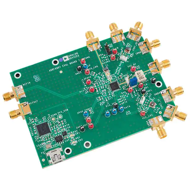
An evaluation board is available for testing the ADRF6807. The
evaluation board schematic is shown in Figure 43.
GND
VCC_RF
Data Sheet
ADRF6807
EVALUATION BOARD LAYOUT AND THERMAL GROUNDING
Table 7 provides the component values and suggestions for
modifying the component values for the various modes of
operation.
09993-042
�Figure 44. Evaluation Board USB Section Schematic
C43
0.1µF
3V3_USB
C41
0.1µF
C53
0.1µF
3V3_USB
3V3_USB
U2
24LC64-I_SN
C42
0.1µF
C55
0.1µF
C44
0.1µF
C46
0.1µF
4 GND
VCC 8
WC_N 7
SCL 6
2 A1
3 A2
SDA 5
1 A0
16
SCL
15
R19
2kΩ
17
3V3_USB
SDA
14 RESERVED
13 IFCLK
12 GND
11 VCC
10 AGND
G3
G4
9 DMINUS
5
G1
G2
8 DPLUS
18
21
C57
0.1µF
C56
10pF
20
C52
1.0µF
3V3_USB
R60
2kΩ
19
R70
140kΩ
25
27
3V3_USB
26
R69
78.7kΩ
C50
1000pF
24
23
3V3_USB
22
4 NC
3 FB
2 OUT2
1 OUT1
28
SD
IN1
IN2
GND
U3
ADP3334
CTL0_FLAGA 29
CTL1_FLAGB 30
CTL2_FLAGC 31
VCC 32
PA0_INT0_N 33
PA1_INT1_N 34
PA2_SLOE 35
PA3_WU2 36
PA5_FIFOARD1 38
PA6_PKTEND 39
PA7_FLAGD_SCLS_N 40
GND 41
PA4_FIFOARD0 37
PB2_FD2
7 AVCC
PB3_FD3
6 AGND
CY7C68013A-56LTXC
U4
3V3_USB
RESET_N 42
43
44
45
46
47
48
49
50
51
52
53
54
PB4_FD4
3
4
3V3_USB
5 XTALIN
4 XTALOUT
3 AVCC
2 RDY1_SLWR
1 RDY0_SLRD
55
VCC
56
GND
CLKOUT
C45
0.1µF
PD7_FD15
PB5_FD5
P5
1
2
C49
0.1µF
2
PD6_FD14
PB0_FD0
GND
R62
100kΩ
PD5_FD13
3V3_USB
PD3_FD11
PD4_FD12
GND
C51
22pF
PD2_FD10
VCC
C48
10pF
4
1
PD1_FD9
VCC
PD0_FD8
PB1_FD1
WAKEUP
PB7_FD7
VCC
PB6_FD6
Rev. B | Page 26 of 36
GND
5V_USB
C54
22pF
3
Y1
24MHz
5
6
7
8
R64
100kΩ
DGND
C47
1.0µF
CR2
R61
2kΩ
C58
0.1µF
CR1
R65
2kΩ
5V_USB
3V3_USB
DATA
CLK
LE
ADRF6807
Data Sheet
09993-144
�Data Sheet
ADRF6807
The package for the ADRF6807 features an exposed paddle on
the underside that should be well soldered to an exposed opening
in the solder mask on the evaluation board. Figure 45 illustrates
the dimensions used in the layout of the ADRF6807 footprint on
the ADRF6807 evaluation board (1 mil = 0.0254 mm).
Note the use of nine via holes on the exposed paddle. These
ground vias should be connected to all other ground layers on
the evaluation board to maximize heat dissipation from the device
package. Under these conditions, the thermal impedance of the
ADRF6807 was measured to be approximately 30°C/W in still air.
09993-044
0.012
0.035
0.050
Figure 46. ADRF6807 Evaluation Board Top Layer
0.168
0.177
0.232
09993-043
0.020
09993-045
0.025
Figure 45. Evaluation Board Layout Dimensions for the ADRF6807 Package
Rev. B | Page 27 of 36
Figure 47. ADRF6807 Evaluation Board Bottom Layer
�ADRF6807
Data Sheet
Table 7. Evaluation Board Configuration Options
Component
VCC, VCC2, VCC_LDO, VCC_LO,
VCC_LO1, VCC_RF, VCC_BB1, 3P3V1,
3P3V2, 3P3V_FORCE, 2P5V, CLK,
DATA, LE, CP, DIG_GND, GND, GND1,
GND2
Function
Power supply, ground and other test points.
Connect a 5 V supply to VCC. Connect a 3.3 V
supply to 3P3V_FORCE.
R1, R6, R7, R8, R13, R14, R15, R17,
R18, R24, R25, R27, R28, R29, R31,
R32, R34, R36, R49
Power supply decoupling. Shorts or power supply
decoupling resistors.
C1, C2, C3, C4, C7, C8, C9, C10, C11,
C12, C16, C17, C18, C19, C20, C21,
C22, C23, C24, C25, C26, C27, C28,
C35, C36, C37, C40
The capacitors provide the required decoupling of
the supply-related pins.
T1, C5, C6
External LO path. The T1 transformer provides
single-ended-to-differential conversion. C5 and C6
provide the necessary ac coupling.
REFIN input path. R26 provides a broadband 50 Ω
termination followed by C31, which provides the
ac coupling into REFIN. R16 provides an external
connectivity to the MUXOUT feature described in
Register 4. R58 provides option for connectivity to
the P1-6 line of a 9-pin D-sub connector for dc
measurements.
Loop filter component options. A variety of loop
filter topologies is supported using component
placements, C13, C14, C15, R9, and R10. R38 and
R59 provide connectivity options to numerous test
points for engineering evaluation purposes. R2
provides resistor programmability of the charge
pump current (see the Register 4—Charge Pump,
PFD, and Reference Path Control section). R37
connects the charge pump output to the loop filter.
R12 references the loop filter to the VCO_LDO.
IF I/Q output paths. The T2 and T3 baluns provide a
9:1 impedance transformation; therefore, with a 50 Ω
load on the single-ended IOUT/QOUT side, the center
tap side of the balun presents a differential 450 Ω
to the ADRF6807. The center taps of the baluns are
ac grounded through C29 and C30. The baluns create
a differential-to-single-ended conversion for ease
of testing and use, but an option to have straight
differential outputs is achieved by populating R3,
R39, R23, and R42 with 0 Ω resistors and removing
R4, R5, R21, and R22. P2 and P3 are differential
measurement test points (not to be used as jumpers).
RF input interface. T4 provides the single-endedto-differential conversion required to drive RFIP and
RFIN. T4 provides a 2:1 impedance transformation.
A single-ended 50 Ω load on the RFIN SMA
connector transforms to a differential 100 Ω
presented across the RFIP (Pin 25) and RFIN (Pin 26)
pins. C38 and C39 are ac coupling capacitors.
R16, R26, R58, C31
R2, R9, R10, R11, R12, R37, R38, R59,
C14, C15, C13
R3, R4, R5, R21, R22, R23, R39, R40,
R41, R42, R43, R44, R45, R46, R47,
R48, C29, C30, T2, T3, P2, P3
C38, C39, T4
Rev. B | Page 28 of 36
Default Condition
VCC, VCC2, VCC_LO, VCC_RF, VCC_BB1,
VCC_LO1, VCO_LDO, 3P3V1, 3P3V2, 2P5V =
Components Corporation TP-104-01-02,
CP, LE, CLK, DATA, 3P3V_FORCE =
Components Corporation TP-104-01-06,
GND, GND1, GND2, DIG_GND =
Components Corporation TP-104-01-00
R1, R6, R7, R8 = 0 Ω (0402),
R13, R14, R15, R17 = 0 Ω (0402),
R18, R24, R25, R27 = 0 Ω (0402),
R28, R29, R31, R32 = 0 Ω (0402),
R34, R36 = 0 Ω (0402),
R49 = open (0402)
C1, C8, C10, C12 = 100 pF (0402),
C16, C18, C21, C22 = 100 pF (0402),
C24, C26 = 100 pF (0402),
C2, C7, C9, C11 = 0.1 μF (0402),
C17, C19, C20, C23 = 0.1 μF (0402),
C25, C40 = 0.1 μF (0402),
C3, C4, C27, C35 = 10 μF (0603),
C36, C37 = 10 μF (0603),
C28 = 10 μF (3216)
C5, C6 = 1 nF (0603),
T1 = TC1-1-13+ Mini-Circuits
R26 = 49.9 Ω (0402),
R16 = 0 Ω (0402),
R58 = open (0402),
C31 = 1 nF (0603)
R12, R37, R38 = 0 Ω (0402),
R59 = open (0402),
R9 = 5.6 kΩ (0402),
R10 = 1.6 kΩ (0402),
R2, R11 = open (0402),
C13 = 62 pF (0402),
C14 = 300 pF (0402),
C15 = 6.2 nF (1206)
R4, R5, R21, R22, = 0 Ω (0402),
R40, R43, R45, R46 = 0 Ω (0402),
R47, R48 = 0 Ω (0402),
R3, R23, R39, R41, R42, R44 = open (0402),
C29, C30, = 0.1 μF (0402),
T2, T3 = TCM9-1+ Mini-Circuits,
P2, P3 = Samtec SSW-102-01-G-S
C38, C39 = 1000 pF (0402),
T4 = ADTL2-18+ Mini-Circuits
�Data Sheet
Component
R50, R51, R52, C32, C33, C34
R33, R55, R56, S1
J1, P1, R62, R63
U2, U3, U4, P5
C41, C42, C43, C44, C46, C53, C55
C48, C49, C45, C56, C57, C58, R19,
R60, R61, R62, R64, CR2
ADRF6807
Function
Serial port interface. Optional RC filters can be
installed on the CLK, DATA, and LE lines to filter the
PC signals through R50 to R52 and C32 to C34. CLK,
DATA, and LE signals can be observed via test points
for debug purposes.
LO select interface. The LOSEL pin, in combination
with the LDRV and LXL bits in Register 5, controls
whether the LOP and LON pins operate as inputs or
outputs. A detailed description of how the LOSEL pin,
LDRV bit, and the LXL bit work together to control
the LOP and LON pins is found in Table 4 under the
LOSEL pin description. Using the S1 switch, the
user can pull LOSEL to a logic high (VCC/2) or a logic
low (ground). Resistors R55 and R56 form a resistor
divider to provide a logic high of VCC/2. LO select
can also be controlled through Pin 9 of J1. The 0 Ω
jumper, R33, must be installed to control LOSEL via J1.
Engineering test points and external control. J1 is a
10-pin connector connected to various important
points on the evaluation board that the user can
measure or force voltages upon. R62 and R63 form
a voltage divider to force a voltage of 1.65 V on
VOCM. Note that Jumper P5 must be connected to
drive VOCM with the resistor divider.
Cypress microcontroller, EEPROM and LDO.
3.3 V supply decoupling. Several capacitors are
used for decoupling on the 3.3 V supply.
Cypress and EEPROM components.
C47, C50, C52, R65, R69, R70, CR1
LDO components.
Y1, C51, C54
Crystal oscillator and components. 24 MHz crystal
oscillator.
Rev. B | Page 29 of 36
Default Condition
R50, R51, R52 = open (0402),
C32, C33, C34 = open (0402)
R33 = 0 Ω (0402),
R55, R56 = 10 kΩ (0402),
S1 = Samtec TSW-103-08-G-S
R62 = R63 = 4.99 kΩ (0402),
P1 = Samtec SSW-102-01-G-S,
J1 = Molex Connector Corp. 10-89-7102
U2 = Microchip MICRO24LC64
U3 = Analog Devices ADP3334ACPZ
U4 = Cypress Semiconductor
CY7C68013A-56LTXC
P5 = Mini USB connector
C41, C42, C43, C44, C46, C53, C55 = 0.1 μF
(0402)
C48, C56 = 10 pF (0402)
C45, C49, C57, C58 = 0.1 μF (0402)
R19, R60, R61 = 2 kΩ (0402)
R62, R64 = 100 kΩ (0402)
CR2 = ROHM SML-21OMTT86
C47, C52 = 1 μF (0402)
C50 = 1000 pF (0402)
R65 = 2 kΩ (0402)
R69 = 78.7 kΩ (0402)
R70 = 140 kΩ (0402)
CR1 = ROHM SML-21OMTT86
Y1 = NDK NX3225SA-24 MHz
C51, C54 = 22 pF (0402)
�ADRF6807
Data Sheet
ADRF6807 SOFTWARE
The ADRF6807 evaluation board can be controlled from PCs
using a USB adapter board, which is also available from Analog
Devices, Inc. The USB adapter evaluation documentation and
ordering information can be found on the EVAL-ADF4XXXZ-USB
product page. The basic user interfaces are shown in Figure 48 and
Figure 49.
09993-148
The software allows the user to configure the ADRF6807 for
various modes of operation. The internal synthesizer is controlled
by clicking any of the numeric values listed in RF Section.
Attempting to program Ref Input Frequency, PFD Frequency,
VCO Frequency (2×LO), LO Frequency, or other values in RF
Section launches the Synth Form window shown in Figure 49.
Using Synth Form, the user can specify values for Local Oscillator
Frequency (MHz) and External Reference Frequency (MHz).
The user can also enable the LO output buffer and divider options
from this menu. After setting the desired values, it is important
to click Upload all registers for the new setting to take effect.
Figure 48. Evaluation Board Software Main Window
Rev. B | Page 30 of 36
�ADRF6807
09993-149
Data Sheet
Figure 49. Evaluation Board Software Synth Form Window
Rev. B | Page 31 of 36
�ADRF6807
Data Sheet
CHARACTERIZATION SETUPS
Figure 50 to Figure 52 show the general characterization bench
setups used extensively for the ADRF6807. The setup shown in
Figure 50 was used to perform the bulk of the testing. An automated
Agilent VEE program was used to control the equipment over the
IEEE bus. This setup was used to measure gain, input P1dB, output
P1dB, input IP2, input IP3, IQ gain mismatch, IQ quadrature
accuracy, and supply current. The evaluation board was used to
perform the characterization with a Mini-Circuits TCM9-1+ balun
on each of the I and Q outputs. When using the TCM9-1+ balun
below 5 MHz (the specified 1 dB low frequency corner of the
balun), distortion performance degrades; however, this is not
the ADRF6807 degrading, merely the low frequency corner of
the balun introducing distortion effects. Through this balun, the
9-to-1 impedance transformation effectively presented a 450 Ω
differential load at each of the I and Q channels. The use of the
broadband Mini-Circuits ADTL2-18+ balun on the input
provided a differential balanced RF input. The losses of both
the input and output baluns were de-embedded from all
measurements.
To perform phase noise and reference spur measurements, the
setup shown in Figure 52 was used. Phase noise was measured
at the baseband output (I or Q) at a baseband carrier frequency
of 50 MHz. The baseband carrier of 50 MHz was chosen to allow
phase noise measurements to be taken at frequencies of up to
20 MHz offset from the carrier. The noise figure was measured
using the setup shown in Figure 51 at a baseband frequency
of 10 MHz.
Rev. B | Page 32 of 36
�Data Sheet
ADRF6807
IEEE
R&S SMA100
SIGNAL GENERATOR
IEEE
3dB
RF1
R&S SMT03 SIGNAL GENERATOR
AGILENT 11636A
POWER DIVIDER
(USED AS COMBINER)
REF
3dB
RF2
IEEE
MINI CIRCUITS
ZHL-42W AMPLIFIER
(SUPPLIED WITH +15VDC
FOR OPERATION)
3dB
3dB
R&S SMT03 SIGNAL GENERATOR
RF
IEEE
CH A
RF SWITCH MATRIX
CH B
HP 8508A
VECTOR
VOLTMETER
IEEE
AGILENT MXA
SPECTRUM ANALYZER
I CH
RF
Q CH
6dB
3dB
6dB
IE EE IEEE
AGILENT 34980A
MULTIFUNCTION
SWITCH
(WITH 34950 AND 2×
34921 MODULES)
AGILENT DMM
(FOR I-5V VP1 MEAS.)
IEEE
AGILENT E3631A
POWER SUPPLY
AGILENT DMM
(FOR I 3.3V VP2 MEAS.)
IEEE
IEEE
I E IEEE
ADRF6807
EVALUATION BOARD
10-PIN
CONNECTION
(+5V VPOS1,
+3.3V VPOS2,
DC MEASURE)
6dB
9-PIN D-SUB CONNECTION
(VCO AND PLL PROGRAMMING)
REF
IEEE
09993-048
IEEE
Figure 50. General Characterization Setup
Rev. B | Page 33 of 36
�ADRF6807
Data Sheet
IEEE
AGILENT 8665B
LOW NOISE SYN
SIGNAL GENERATOR
REF
RF1
AGILENT 346B
NOISESOURCE
3dB
RF
RF SWITCH MATRIX
10MHz
LOW-PASS FILTER
IEEE
AGILENT N8974A
NOISE FIGURE ANALYZER
I CH
RF
Q CH
6dB
3dB
6dB
AGILENT DMM
(FOR I-5V VP1 MEAS.)
E IEEE
AGILENT 34980A
MULTIFUNCTION
SWITCH
(WITH 34950 AND 2×
34921 MODULES)
IEEE
I E IEEE
AGILENT DMM
(FOR I 3.3V VP2 MEAS.)
IEEE
IEEE
AGILENT E3631A
POWER SUPPLY
ADRF6807
EVALUATION BOARD
10-PIN
CONNECTION
(+5V VPOS1,
+3.3V VPOS2,
DC MEASURE)
6dB
9-PIN D-SUB CONNECTION
(VCO AND PLL PROGRAMMING)
REF
IEEE
09993-049
IEEE
Figure 51. Noise Figure Characterization Setup
Rev. B | Page 34 of 36
�Data Sheet
ADRF6807
IEEE
R&S SMA100
SIGNAL GENERATOR
IEEE
REF
RF1
R&S SMA100
SIGNAL GENERATOR
IEEE
100MHz
LOW-PASS FILTER
3dB
AGILENT E5052 SIGNAL SOURCE
ANALYZER
RF
RF SWITCH MATRIX
IEEE
AGILENT MXA
SPECTRUM ANALYZER
I CH
RF
Q CH
6dB
3dB
6dB
AGILENT DMM
(FOR I-5V VP1 MEAS.)
E IEEE
AGILENT 34980A
MULTIFUNCTION
SWITCH
(WITH 34950 AND 2×
34921 MODULES)
IEEE
AGILENT E3631A
POWER SUPPLY
AGILENT DMM
(FOR I 3.3V VP2 MEAS.)
IEEE
IEEE
I E IEEE
ADRF6807
EVALUATION BOARD
10-PIN
CONNECTION
(+5V VPOS1,
+3.3V VPOS2,
DC MEASURE)
6dB
9-PIN D-SUB CONNECTION
(VCO AND PLL PROGRAMMING)
REF
IEEE
09993-050
IEEE
Figure 52. Phase Noise Characterization Setup
Rev. B | Page 35 of 36
�ADRF6807
Data Sheet
OUTLINE DIMENSIONS
6.00
BSC SQ
TOP
VIEW
5.75
BSC SQ
0.50
BSC
29
28
40
1
4.45
4.30 SQ
4.15
EXPOSED
PAD
(BOT TOM VIEW)
0.50
0.40
0.30
1.00
0.85
0.80
0.05 MAX
0.02 NOM
COPLANARITY
0.08
0.20 REF
0.30
0.23
0.18
SEATING
PLANE
11
10
0.25 MIN
4.50
REF
0.80 MAX
0.65 TYP
12° MAX
20
19
PIN 1
INDICATOR
FOR PROPER CONNECTION OF
THE EXPOSED PAD, REFER TO
THE PIN CONFIGURATION AND
FUNCTION DESCRIPTIONS
SECTION OF THIS DATA SHEET.
COMPLIANT TO JEDEC STANDARDS MO-220-VJJD-2
122107-A
PIN 1
INDICATOR
0.60 MAX
0.60 MAX
Figure 53. 40-Lead Lead Frame Chip Scale Package [LFCSP_VQ]
6 mm × 6 mm Body, Very Thin Quad
(CP-40-4)
Dimensions shown in millimeters
ORDERING GUIDE
Model 1
ADRF6807ACPZ-R7
ADRF6807-EVALZ
1
Temperature Range
−40°C to +85°C
Package Description
40-Lead Lead Frame Chip Scale Package [LFCSP_VQ]
Evaluation Board
Z = RoHS Compliant Part.
©2011–2012 Analog Devices, Inc. All rights reserved. Trademarks and
registered trademarks are the property of their respective owners.
D09993-0-2/12(B)
Rev. B | Page 36 of 36
Package Option
CP-40-4
Ordering
Quantity
750
�