a
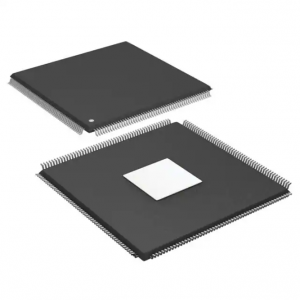
SUMMARY High Performance Signal Computer for Speech, Sound, Graphics and Imaging Applications Super Harvard Architecture Computer (SHARC)— Four Independent Buses for Dual Data, Instructions, and I/O 32-Bit IEEE Floating-Point Computation Units— Multiplier, ALU and Shifter 1 Megabit On-Chip SRAM Memory and Integrated I/O Peripherals—A Complete System-On-A-Chip Integrated Multiprocessing Features KEY FEATURES 50 MIPS, 20 ns Instruction Rate, Single-Cycle Instruction Execution 120 MFLOPS Peak, 80 MFLOPS Sustained Performance Dual Data Address Generators with Modulo and BitReverse Addressing Efficient Program Sequencing with Zero-Overhead Looping: Single-Cycle Loop Setup IEEE JTAG Standard 1149.1 Test Access Port and On-Chip Emulation 240-Lead MQFP Package 225-Ball Plastic Ball Grid Array (PBGA)
CORE PROCESSOR
TIMER INSTRUCTION CACHE
32 x 48-BIT ADDR ADDR
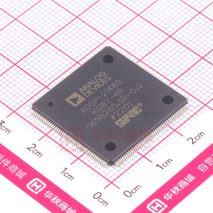
ADSP-2106x SHARC® DSP Microcomputer Family ADSP-21061/ADSP-21061L
Pin-Compatible with ADSP-21060 (4 Mbit) and ADSP-21062 (2 Mbit) Flexible Data Formats and 40-Bit Extended Precision 32-Bit Single-Precision and 40-Bit Extended-Precision IEEE Floating-Point Data Formats 32-Bit Fixed-Point Data Format, Integer and Fractional, with 80-Bit Accumulators
Parallel Computations Single-Cycle Multiply and ALU Operations in Parallel with Dual Memory Read/Writes and Instruction Fetch Multiply with Add and Subtract for Accelerated FFT Butterfly Computation 1024-Point Complex FFT Benchmark: 0.37 ms (18,221 Cycles) 1 Megabit Configurable On-Chip SRAM Dual-Ported for Independent Access by Core Processor and DMA Configurable as 32K Words Data Memory (32-Bit), 16K Words Program Memory (48-Bit) or Combinations of Both Up to 1 Mbit Off-Chip Memory Interfacing 4-Gigawords Addressable (32-Bit Address) Programmable Wait State Generation, Page-Mode DRAM Support
DUAL-PORTED SRAM
BLOCK 0 BLOCK 1
TWO INDEPENDENT DUAL-PORTED BLOCKS PROCESSOR PORT
DATA DATA
JTAG
TEST & EMULATION
7
I/O PORT
DATA DATA ADDR ADDR
DAG1
8 x 4 x 32
DAG2
8 x 4 x 24
PROGRAM SEQUENCER 24 32 IOD 48 IOA 17
PM ADDRESS BUS DM ADDRESS BUS
EXTERNAL PORT
ADDR BUS MUX MULTIPROCESSOR INTERFACE 32
PM DATA BUS
48 40/32 DATA BUS MUX HOST PORT 48
BUS CONNECT (PX)
DM DATA BUS
DATA REGISTER FILE MULTIPLIER
16 x 40-BIT
IOP REGISTERS BARREL SHIFTER ALU (MEMORY MAPPED) CONTROL, STATUS & DATA BUFFERS
DMA CONTROLLER SERIAL PORTS (2)
4 6 6
I/O PROCESSOR
Figure 1. ADSP-21061/ADSP-21061L Block Diagram
SHARC is a registered trademark of Analog Devices, Inc.
R EV. B
Information furnished by Analog Devices is believed to be accurate and reliable. However, no responsibility is assumed by Analog Devices for its use, nor for any infringements of patents or other rights of third parties which may result from its use. No license is granted by implication or otherwise under any patent or patent rights of Analog Devices. One Technology Way, P.O. Box 9106, Norwood, MA 02062-9106, U.S.A. Tel: 781/329-4700 World Wide Web Site: http://www.analog.com Fax: 781/326-8703 © Analog Devices, Inc., 2000
�ADSP-21061/ADSP-21061L
DMA Controller 6 DMA Channels Background DMA Transfers at 50 MHz, in Parallel with Full-Speed Processor Execution Performs Transfers Between ADSP-21061 Internal Memory and External Memory, External Peripherals, Host Processor, or Serial Ports Host Processor Interface Efficient Interface to 16- and 32-Bit Microprocessors Host can Directly Read/Write ADSP-21061 Internal Memory Multiprocessing Glueless Connection for Scalable DSP Multiprocessing Architecture Distributed On-Chip Bus Arbitration for Parallel Bus Connect of Up To Six ADSP-21061s Plus Host 300 Mbytes/s Transfer Rate Over Parallel Bus Serial Ports Two 40 Mbit/s Synchronous Serial Ports Independent Transmit and Receive Functions 3- to 32-Bit Data Word Width -Law/A-Law Hardware Companding TDM Multichannel Mode Multichannel Signaling Protocol
TABLE OF CONTENTS GENERAL DESCRIPTION . . . . . . . . . . . . . . . . . . . . . . . . . 3 ADSP-21000 FAMILY CORE ARCHITECTURE . . . . . . . 4 ADSP-21061 FEATURES . . . . . . . . . . . . . . . . . . . . . . . . . . 4 DEVELOPMENT TOOLS . . . . . . . . . . . . . . . . . . . . . . . . . . 8 ADDITIONAL INFORMATION . . . . . . . . . . . . . . . . . . . . . 8 PIN DESCRIPTIONS . . . . . . . . . . . . . . . . . . . . . . . . . . . . . 9 TARGET BOARD CONNECTOR FOR EZ-ICE® PROBE . . . . . . . . . . . . . . . . . . . . . . . . . . . . . . . . . . . . . . 12 RECOMMENDED OPERATING CONDITIONS (5 V) . 14 ELECTRICAL CHARACTERISTICS (5 V) . . . . . . . . . . . 14 POWER DISSIPATION ADSP-21061 (5 V) . . . . . . . . . . . . 15 RECOMMENDED OPERATING CONDITIONS (3.3 V) 16 ELECTRICAL CHARACTERISTICS (3.3 V) . . . . . . . . . . 16 POWER DISSIPATION ADSP-21061L (3.3 V) . . . . . . . . . 17 ABSOLUTE MAXIMUM RATINGS . . . . . . . . . . . . . . . . 18 TIMING SPECIFICATIONS . . . . . . . . . . . . . . . . . . . . . . . 18 Memory Read—Bus Master . . . . . . . . . . . . . . . . . . . . . . . 21 Memory Write—Bus Master . . . . . . . . . . . . . . . . . . . . . . 22 Synchronous Read/Write—Bus Master . . . . . . . . . . . . . . 23 Synchronous Read/Write—Bus Slave . . . . . . . . . . . . . . . . 25 Multiprocessor Bus Request and Host Bus Request . . . . . 26 Asynchronous Read/Write—Host to ADSP-21061 . . . . . . 28 Three-State Timing—Bus Master, Bus Slave, HBR, SBTS . . . . . . . . . . . . . . . . . . . . . . . . . . . . . . . . . 30 DMA Handshake . . . . . . . . . . . . . . . . . . . . . . . . . . . . . . . 32 Serial Ports . . . . . . . . . . . . . . . . . . . . . . . . . . . . . . . . . . . . 34 JTAG Test Access Port and Emulation . . . . . . . . . . . . . . . 37 OUTPUT DRIVE CURRENTS . . . . . . . . . . . . . . . . . . . . . 38 POWER DISSIPATION . . . . . . . . . . . . . . . . . . . . . . . . . . . 38 TEST CONDITIONS . . . . . . . . . . . . . . . . . . . . . . . . . . . . 38 ENVIRONMENTAL CONDITIONS . . . . . . . . . . . . . . . . 41 240-LEAD METRIC MQFP PIN CONFIGURATIONS . . 42 OUTLINE DIMENSIONS . . . . . . . . . . . . . . . . . . . . . . 43, 44 ADSP-21061L 225-Ball Plastic Ball Grid Array (PBGA) Package Pinout . . . . . . . . . . . . . . . . . . . . . . . . . . . . . . . . . 45 225-Ball Plastic Ball Grid Array (PBGA) Package Pinout . . . . . 46 OUTLINE DIMENSIONS . . . . . . . . . . . . . . . . . . . . . . . . . 47 ORDERING GUIDE . . . . . . . . . . . . . . . . . . . . . . . . . . . . . 47
FIGURES
Figure 1. Figure 2. Figure 3. Figure 4. Figure 5.
ADSP-21061/ADSP-21061L Block Diagram . . . . ADSP-21061/ADSP-21061L System . . . . . . . . . . . Multiprocessing System . . . . . . . . . . . . . . . . . . . . . ADSP-21061/ADSP-21061L Memory Map . . . . . Target Board Connector For ADSP-21061/
1 4 6 7
EZ-ICE is a registered trademark of Analog Devices, Inc.
ADSP-21061L EZ-ICE Emulator (Jumpers in Place) . . . 12 Figure 6. JTAG Scan Path Connections for Multiple ADSP-21061/ADSP-21061L Systems . . . . . . . . . . . . . . . 12 Figure 7. JTAG Clocktree for Multiple ADSP-21061/ ADSP-21061L Systems . . . . . . . . . . . . . . . . . . . . . . . . . . 13 Figure 8. Clock Input . . . . . . . . . . . . . . . . . . . . . . . . . . . . . 19 Figure 9. Reset . . . . . . . . . . . . . . . . . . . . . . . . . . . . . . . . . . 19 Figure 10. Interrupts . . . . . . . . . . . . . . . . . . . . . . . . . . . . . . 20 Figure 11. Timer . . . . . . . . . . . . . . . . . . . . . . . . . . . . . . . . 20 Figure 12. Flags . . . . . . . . . . . . . . . . . . . . . . . . . . . . . . . . . 20 Figure 13. Memory Read—Bus Master . . . . . . . . . . . . . . . . 21 Figure 14. Memory Write—Bus Master . . . . . . . . . . . . . . . 22 Figure 15. Synchronous Read/Write—Bus Master . . . . . . . 24 Figure 16. Synchronous Read/Write—Bus Slave . . . . . . . . . 25 Figure 17. Multiprocessor Bus Request and Host Bus Request . . . . . . . . . . . . . . . . . . . . . . . . . . . . . . . . . . . . . . 27 Figure 18a. Synchronous REDY Timing . . . . . . . . . . . . . . 28 Figure 18b. Asynchronous Read/Write—Host to ADSP-21061/ADSP-21061L . . . . . . . . . . . . . . . . . . . . . . 29 Figure 19a. Three-State Timing (Bus Transition Cycle, SBTS Assertion) . . . . . . . . . . . . . . . . . . . . . . . . . . . . . . . 31 Figure 19b. Three-State Timing (Host Transition Cycle) . . 31 Figure 20. DMA Handshake Timing . . . . . . . . . . . . . . . . . 33 Figure 21. Serial Ports . . . . . . . . . . . . . . . . . . . . . . . . . . . . 35 Figure 22. External Late Frame Sync . . . . . . . . . . . . . . . . . 36 Figure 23. JTAG Test Access Port and Emulation . . . . . . . 37 Figure 24. Output Enable/Disable . . . . . . . . . . . . . . . . . . . 39 Figure 25. Equivalent Device Loading for AC Measurements (Includes All Fixtures) . . . . . . . . . . . . . . . . . . . . . . . . . . . 39 Figure 26. Voltage Reference Levels for AC Measurements (Except Output Enable/Disable) . . . . . . . . . . . . . . . . . . . . 39 Figure 27. ADSP-2106x Typical Drive Currents (VDD = 5 V) . . . . . . . . . . . . . . . . . . . . . . . . . . . . . . . . . . . 40 Figure 28. Typical Output Rise Time (10%–90% VDD) vs. Load Capacitance (VDD = 5 V) . . . . . . . . . . . . . . . . . . . . 40 Figure 29. Typical Output Rise Time (0.8 V–2.0 V) vs. Load Capacitance (VDD = 5 V) . . . . . . . . . . . . . . . . . . . . . . . . . 40 Figure 30. Typical Output Delay or Hold vs. Load Capacitance (at Maximum Case Temperature) (VDD = 5 V) . . . . . . . . 40 Figure 31. ADSP-2106x Typical Drive Currents (VDD = 3.3 V) . . . . . . . . . . . . . . . . . . . . . . . . . . . . . . . . . . 40 Figure 32. Typical Output Rise Time (10%–90% VDD) vs. Load Capacitance (VDD = 3.3 V) . . . . . . . . . . . . . . . . . . . 40 Figure 33. Typical Output Rise Time (0.8 V–2.0 V) vs. Load Capacitance (VDD = 3.3 V) . . . . . . . . . . . . . . . . . . . . . . . 41 Figure 34. Typical Output Delay or Hold vs. Load Capacitance (at Maximum Case Temperature) (VDD = 3.3 V) . . . . . . . 41 – 2– REV. B
�ADSP-21061/ADSP-21061L
S
GENERAL NOTE GENERAL DESCRIPTION
®
This data sheet represents production released specifications for the ADSP-21061 5 V and ADSP-21061L 3.3 V processors. ADSP-21061 is used throughout this data sheet to refer to both devices unless expressly noted.
Figure 1 shows a block diagram of the ADSP-21061/ADSP21061L, illustrating the following architectural features: Computation Units (ALU, Multiplier and Shifter) with a Shared Data Register File Data Address Generators (DAG1, DAG2) Program Sequencer with Instruction Cache Interval Timer 1 Mbit On-Chip SRAM External Port for Interfacing to Off-Chip Memory and Peripherals Host Port & Multiprocessor Interface DMA Controller Serial Ports JTAG Test Access Port Figure 2 shows a typical single-processor system. A multiprocessing system is shown in Figure 3.
Table I. ADSP-21061/ADSP-21061L Benchmarks (@ 50 MHz)
The ADSP-21061 is a member of the powerful SHARC family of floating point processors. The SHARC—Super Harvard Architecture Computer—are signal processing microcomputers that offer new capabilities and levels of integration and performance. The ADSP-21061 is a 32-bit processor optimized for high performance DSP applications. The ADSP-21061 combines the ADSP-21000 DSP core with a dual-ported on-chip SRAM and an I/O processor with a dedicated I/O bus to form a complete system-in-a-chip. Fabricated in a high-speed, low-power CMOS process, the ADSP-21061 has a 20 ns instruction cycle time operating at up to 50 MIPS. With its on-chip instruction cache, the processor can execute every instruction in a single cycle. Table I shows performance benchmarks for the ADSP-21061/ADSP-21061L. The ADSP-21061 SHARC combines a high-performance floating-point DSP core with integrated, on-chip system features, including a 1 Mbit SRAM memory, host processor interface, DMA controller, serial ports and parallel bus connectivity for glueless DSP multiprocessing.
1024-Pt. Complex FFT (Radix 4, with Digit Reverse) FIR Filter (per Tap) IIR Filter (per Biquad) Divide (y/x) Inverse Square Root (1/√x) DMA Transfer Rate
0.37 ms 20 ns 80 ns 120 ns 180 ns 300 Mbytes/s
18,221 Cycles 1 Cycle 4 Cycles 6 Cycles 9 Cycles
REV. B
–3–
�ADSP-21061/ADSP-21061L
ADSP-21000 FAMILY CORE ARCHITECTURE Instruction Cache
The ADSP-21061 includes the following architectural features of the ADSP-21000 family core. The ADSP-21061 is code and function compatible with the ADSP-21060/ADSP-21062 and the ADSP-21020.
Independent, Parallel Computation Units
The arithmetic/logic unit (ALU), multiplier and shifter all perform single-cycle instructions. The three units are arranged in parallel, maximizing computational throughput. Single multifunction instructions execute parallel ALU and multiplier operations. These computation units support IEEE 32-bit singleprecision floating-point, extended precision 40-bit floatingpoint and 32-bit fixed-point data formats.
ADSP-21061/ ADSP-21061L
CONTROL ADDRESS 1x CLOCK TO GND 3 4 CLKIN EBOOT LBOOT IRQ2-0 FLAG3-0 TIMEXP TCLK0 RCLK0 TFS0 RSF0 DT0 DR0 ADDR31-0 DATA47-0 RD WR ACK MS3-0 PAGE SBTS SW ADRCLK DMAR1-2 DMAG1-2 CS HBR HBG REDY BR1-6 CPA JTAG 7 HOST PROCESSOR INTERFACE (OPTIONAL) ADDR DATA BMS CS ADDR DATA DATA ADDR MEMORY AND OE PERIPHERALS WE (OPTIONAL) ACK DATA CS BOOT EPROM (OPTIONAL)
The ADSP-21061 includes an on-chip instruction cache that enables three-bus operation for fetching an instruction and two data values. The cache is selective—only the instructions whose fetches conflict with PM bus data accesses are cached. This allows full-speed execution of core, looped operations such as digital filter multiply-accumulates and FFT butterfly processing.
Data Address Generators with Hardware Circular Buffers
The ADSP-21061’s two data address generators (DAGs) implement circular data buffers in hardware. Circular buffers allow efficient programming of delay lines and other data structures required in digital signal processing, and are commonly used in digital filters and Fourier transforms. The ADSP-21061 two DAGs contain sufficient registers to allow the creation of up to 32 circular buffers (16 primary register sets, 16 secondary). The DAGs automatically handle address pointer wraparound, reducing overhead, increasing performance and simplifying implementation. Circular buffers can start and end at any memory location.
Flexible Instruction Set
SERIAL DEVICE (OPTIONAL)
The 48-bit instruction word accommodates a variety of parallel operations, for concise programming. For example, the ADSP21061 can conditionally execute a multiply, an add, a subtract and a branch, all in a single instruction.
ADSP-21061 FEATURES
DMA DEVICE (OPTIONAL) DATA
Augmenting the ADSP-21000 family core, the ADSP-21061 adds the following architectural features:
Dual-Ported On-Chip Memory
SERIAL DEVICE (OPTIONAL)
TCLK1 RCLK1 TFS1 RSF1 DT1 DR1
RPBA ID2-0 RESET
The ADSP-21061 contains 1 megabit of on-chip SRAM, organized as two banks of 0.5 Mbits each. Each bank has eight 16bit columns with 4K 16-bit words per column. Each memory block is dual-ported for single-cycle, independent accesses by the core processor and I/O processor or DMA controller. The dual-ported memory and separate on-chip buses allow two data transfers from the core and one from I/O, all in a single cycle (see Figure 4 for the ADSP-21061 Memory Map). On the ADSP-21061, the memory can be configured as a maximum of 32K words of 32-bit data, 64K words for 16-bit data, 16K words of 48-bit instructions (and 40-bit data) or combinations of different word sizes up to 1 megabit. All the memory can be accessed as 16-bit, 32-bit or 48-bit. A 16-bit floating-point storage format is supported that effectively doubles the amount of data that may be stored on chip. Conversion between the 32-bit floating-point and 16-bit floatingpoint formats is done in a single instruction. While each memory block can store combinations of code and data, accesses are most efficient when one block stores data, using the DM bus for transfers, and the other block stores instructions and data, using the PM bus for transfers. Using the DM and PM buses in this way, with one dedicated to each memory block, assures single-cycle execution with two data transfers. In this case, the instruction must be available in the cache. Single-cycle execution is also maintained when one of the data operands is transferred to or from off-chip, via the ADSP21061’s external port.
Figure 2. ADSP-21061/ADSP-21061L System
Data Register File
A general purpose data register file is used for transferring data between the computation units and the data buses, and for storing intermediate results. This 10-port, 32-register (16 primary, 16 secondary) register file, combined with the ADSP21000 Harvard architecture, allows unconstrained data flow between computation units and internal memory.
Single-Cycle Fetch of Instruction and Two Operands
The ADSP-21061 features an enhanced Harvard architecture in which the data memory (DM) bus transfers data and the program memory (PM) bus transfers both instructions and data (see Figure 1). With its separate program and data memory buses and on-chip instruction cache, the processor can simultaneously fetch two operands and an instruction (from the cache), all in a single cycle.
– 4–
REV. B
�ADSP-21061/ADSP-21061L
Off-Chip Memory and Peripherals Interface
The ADSP-21061’s external port provides the processor’s interface to off-chip memory and peripherals. The 4-gigaword offchip address space is included in the ADSP-21061’s unified address space. The separate on-chip buses—for program memory, data memory and I/O—are multiplexed at the external port to create an external system bus with a single 32-bit address bus and a single 48-bit (or 32-bit) data bus. The on-chip Super Harvard Architecture provides three-bus performance, while the off-chip unified address space gives flexibility to the designer. Addressing of external memory devices is facilitated by on-chip decoding of high order address lines to generate memory bank select signals. Separate control lines are also generated for simplified addressing of page-mode DRAM. The ADSP-21061 provides programmable memory wait states and external memory acknowledge controls to allow interfacing to DRAM and peripherals with variable access, hold and disable time requirements.
Host Processor Interface
Six channels of DMA are available on the ADSP-21061—four via the serial ports, and two via the processor’s external port (for either host processor, other ADSP-21061s, memory or I/O transfers). Programs can be downloaded to the ADSP-21061 using DMA transfers. Asynchronous off-chip peripherals can control two DMA channels using DMA Request/Grant lines (DMAR1-2, DMAG1-2). Other DMA features include interrupt generation upon completion of DMA transfers and DMA chaining for automatic linked DMA transfers.
Serial Ports
The ADSP-21061 features two synchronous serial ports that provide an inexpensive interface to a wide variety of digital and mixed-signal peripheral devices. The serial ports can operate at the full clock rate of the processor, providing each with a maximum data rate of 40 Mbit/s. Independent transmit and receive functions provide greater flexibility for serial communications. Serial port data can be automatically transferred to and from on-chip memory via DMA. Each of the serial ports offers TDM multichannel mode. The serial ports can operate with little-endian or big-endian transmission formats, with word lengths selectable from three bits to 32 bits. They offer selectable synchronization and transmit modes as well as optional µ-law or A-law companding. Serial port clocks and frame syncs can be internally or externally generated. The serial ports also include keyword and keymask features to enhance interprocessor communication.
Multiprocessing
The ADSP-21061’s host interface allows easy connection to standard microprocessor buses, both 16-bit and 32-bit, with little additional hardware required. Asynchronous transfers at speeds up to the full clock rate of the processor are supported. The host interface is accessed through the ADSP-21061’s external port and is memory-mapped into the unified address space. Two channels of DMA are available for the host interface; code and data transfers are accomplished with low software overhead. The host processor requests the ADSP-21061’s external bus with the host bus request (HBR), host bus grant (HBG) and ready (REDY) signals. The host can directly read and write the internal memory of the ADSP-21061, and can access the DMA channel setup and mailbox registers. Vector interrupt support is provided for efficient execution of host commands.
DMA Controller
The ADSP-21061’s on-chip DMA controller allows zerooverhead, nonintrusive data transfers without processor intervention. The DMA controller operates independently and invisibly to the processor core, allowing DMA operations to occur while the core is simultaneously executing its program instructions. DMA transfers can occur between the ADSP-21061’s internal memory and either external memory, external peripherals, or a host processor. DMA transfers can also occur between the ADSP-21061’s internal memory and its serial ports. DMA transfers between external memory and external peripheral devices are another option. External bus packing to 16-, 32or 48-bit words is performed during DMA transfers.
The ADSP-21061 offers powerful features tailored to multiprocessing DSP systems. The unified address space allows direct interprocessor accesses of each ADSP-21061’s internal memory. Distributed bus arbitration logic is included on-chip for simple, glueless connection of systems containing up to six ADSP-21061s and a host processor. Master processor changeover incurs only one cycle of overhead. Bus arbitration is selectable as either fixed or rotating priority. Bus lock allows indivisible read-modifywrite sequences for semaphores. A vector interrupt is provided for interprocessor commands. Maximum throughput for interprocessor data transfer is 500 Mbytes/sec over the external port. Broadcast writes allow simultaneous transmission of data to all ADSP-21061s and can be used to implement reflective semaphores.
Program Booting
The internal memory of the ADSP-21061 can be booted at system power-up from either an 8-bit EPROM or a host processor. Selection of the boot source is controlled by the BMS (Boot Memory Select), EBOOT (EPROM Boot), and LBOOT (Host Boot) pins. 32-bit and 16-bit host processors can be used for booting. See the BMS pin in the Pin Function Descriptions section of this data sheet.
REV. B
–5–
�ADSP-21061/ADSP-21061L
CONTROL ADDRESS ADDRESS
ADSP-2106x #6 ADSP-2106x #5 ADSP-2106x #4 ADSP-2106x #3
CLKIN RESET RPBA 011 3 ID 2-0 CONTROL ADDR31-0 DATA47-0
CPA BR1-2, BR4-6 BR3
5
ADSP-2106x #2
CLKIN RESET RPBA 3 010 ID 2-0 CONTROL ADDR31-0 DATA47-0
CPA BR1, BR3-6 BR2
5
CONTROL
ADSP-2106x #1
1x CLOCK RESET CLKIN ADDR31-0 RESET RPBA 3 001 ID 2-0 DATA47-0 RD WR ACK MS3-0 BMS PAGE SBTS SW ADRCLK CS HBR HBG REDY CPA BR2-6 BR1 5
DATA
DATA
ADDR DATA OE WE ACK CS CS ADDR DATA GLOBAL MEMORY AND PERIPHERALS (OPTIONAL)
CONTROL
BOOT EPROM (OPTIONAL)
HOST PROCESSOR INTERFACE (OPTIONAL) ADDR DATA
Figure 3. Multiprocessing System
– 6–
REV. B
�ADSP-21061/ADSP-21061L
0x0000 0000 IOP REGISTERS 0x0040 0000 BANK 0 DRAM (OPTIONAL) MS0
INTERNAL MEMORY SPACE
0x0002 0000 NORMAL WORD ADDRESSING 0x0004 0000 SHORT WORD ADDRESSING 0x0008 0000 INTERNAL MEMORY SPACE OF ADSP-2106x WITH ID=001 0x0010 0000 INTERNAL MEMORY SPACE OF ADSP-2106x WITH ID=010 0x0018 0000 INTERNAL MEMORY SPACE OF ADSP-2106x WITH ID=011 0x0020 0000
BANK 1
MS1
BANK 2
MS2
MULTIPROCESSOR MEMORY SPACE
INTERNAL MEMORY SPACE OF ADSP-2106x WITH ID=100 0x0028 0000 INTERNAL MEMORY SPACE OF ADSP-2106x WITH ID=101 0x0030 0000 INTERNAL MEMORY SPACE OF ADSP-2106x WITH ID=110 0x0038 0000 BROADCAST WRITE TO ALL ADSP-2106xs 0x003F FFFF
EXTERNAL MEMORY SPACE
BANK 3 MS3
BANK SIZE IS SELECTED BY MSIZE BIT FIELD OF SYSCON REGISTER. NONBANKED
NORMAL WORD ADDRESSING: 32-BIT DATA WORDS 48-BIT INSTRUCTION WORDS SHORT WORD ADDRESSING: 16-BIT DATA WORDS
0xFFFF FFFF
Figure 4. ADSP-21061/ADSP-21061L Memory Map
REV. B
–7–
�ADSP-21061/ADSP-21061L
Porting Code from ADSP-21060 or ADSP-21062 to the ADSP-21061
The ADSP-21061 is pin compatible with the ADSP-21060/ ADSP-21061/ADSP-21062 processors. The ADSP-21061 pins that correspond to the Link Port pins of the ADSP-21060/ ADSP-21062 are no-connects. The ADSP-21061 is object code compatible with the ADSP21060/ADSP-21062 except for the following functional changes: The ADSP-21061 memory is organized into two blocks with eight columns that are 4K deep per block. The ADSP-21060/ADSP-21062 memory has 16 columns per block. Link port functions are not available. Handshake external port DMA pins DMAR2 and DMAG2 are assigned to external port DMA Channel 6 instead of Channel 8. 2-D DMA capability of the SPORT is not available. The modify registers in SPORT DMA are not programmable. On the ADSP-21061, Block 0 starts at the beginning of internal memory, normal word address 0x0002 0000. Block 1 starts at the end of Block 0, with contiguous addresses. The remaining addresses in internal memory are divided into blocks that alias into Block 1. This allows any code or data stored in Block 1 on the ADSP-21062 to retain the same addresses on the ADSP21061—these addresses will alias into the actual Block 1 of each processor. If you develop your application using the ADSP-21062, but will migrate to the ADSP-21061, use only the first eight columns of each memory bank. Limit your application to 8K of instructions or up to 16K of data in each bank of the ADSP-21062, or any combinations of instructions or data that does not exceed the memory bank.
DEVELOPMENT TOOLS
The same EZ-ICE hardware can be used for the ADSP-21060/ ADSP-21062, to fully emulate the ADSP-21061, with the exception of displaying and modifying the two new SPORTS registers. The emulator will not display these two registers, but your code can use them. Analog Devices ADSP-21000 Family Development Software includes an easy to use Assembler based on an algebraic syntax, Assembly Library/Librarian, Linker, instruction-level Simulator, an ANSI C optimizing Compiler, the CBUG™ C Source— Level Debugger and a C Runtime Library including DSP and mathematical functions. The Optimizing Compiler includes Numerical C extensions based on the work of the ANSI Numerical C Extensions Group. Numerical C provides extensions to the C language for array selections, vector math operations, complex data types, circular pointers and variably dimensioned arrays. The ADSP-21000 Family Development Software is available for both the PC and Sun platforms. The EZ-ICE Emulator uses the IEEE 1149.1 JTAG test access port of the ADSP-21061 processor to monitor and control the target board processor during emulation. The EZ-ICE provides full-speed emulation, allowing inspection and modification of memory, registers, and processor stacks. Nonintrusive in-circuit emulation is assured by the use of the processor’s JTAG interface—the emulator does not affect target system loading or timing. Further details and ordering information are available in the ADSP-21000 Family Hardware and Software Development Tools data sheet (ADDS-210xx-TOOLS). This data sheet can be requested from any Analog Devices sales office or distributor. In addition to the software and hardware development tools available from Analog Devices, third parties provide a wide range of tools supporting the SHARC processor family. Hardware tools include SHARC PC plug-in cards multiprocessor SHARC VME boards, and daughter and modules with multiple SHARCs and additional memory. These modules are based on the SHARCPAC™ module specification. Third Party software tools include an Ada compiler, DSP libraries, operating systems and block diagram design tools.
ADDITIONAL INFORMATION
The ADSP-21061 is supported with a complete set of software and hardware development tools, including an EZ-ICE InCircuit Emulator, EZ-Kit Lite, and development software. The SHARC EZ-Kit Lite (ADDS-2106x-EZ-Lite) is a complete low cost package for DSP evaluation and prototyping. The EZ-Kit Lite contains an evaluation board with an ADSP-21061 (5 V) processor and provides a serial connection to your PC. The EZKit Lite also includes an optimizing compiler, assembler, instruction level simulator, run-time libraries, diagnostic utilities and a complete set of example programs.
This data sheet provides a general overview of the ADSP-21061 architecture and functionality. For detailed information on the ADSP-21000 Family core architecture and instruction set, refer to the ADSP-2106x SHARC User’s Manual, Second Edition.
CBUG and SHARCPAC are trademarks of Analog Devices, Inc.
– 8–
REV. B
�ADSP-21061/ADSP-21061L
PIN DESCRIPTIONS
ADSP-21061 pin definitions are listed below. Inputs identified as synchronous (S) must meet timing requirements with respect to CLKIN (or with respect to TCK for TMS, TDI). Inputs identified as asynchronous (A) can be asserted asynchronously to CLKIN (or to TCK for TRST). Unused inputs should be tied or pulled to IVDD or IGND, except for ADDR31-0, DATA47-0, FLAG3-0, SW and inputs that have internal pull-up or pull-down resistors (CPA, ACK, DTx,
DRx, TCLKx, RCLKx, TMS and TDI)—these pins can be left floating. These pins have a logic-level hold circuit that prevents the input from floating internally. I = Input S = Synchronous P = Power Supply (O/D) = Open Drain O = Output A = Asynchronous G = Ground (A/D) = Active Drive T = Three-State (when SBTS is asserted, or when the ADSP-2106x is a bus slave)
PIN FUNCTION DESCRIPTIONS
Pin ADDR31-0
Type I/O/T
Function External Bus Address. The ADSP-21061 outputs addresses for external memory and peripherals on these pins. In a multiprocessor system the bus master outputs addresses for read/writes of the internal memory or IOP registers of other ADSP-2106xs. The ADSP-21061 inputs addresses when a host processor or multiprocessing bus master is reading or writing its internal memory or IOP registers. External Bus Data. The ADSP-21061 inputs and outputs data and instructions on these pins. The external data bus transfers 32-bit single-precision floating-point data and 32-bit fixed-point data over Bits 47-16. 40-bit extended-precision floating-point data is transferred over Bits 47-8 of the bus. 16-bit short word data is transferred over Bits 31-16 of the bus. Pull-up resistors on unused DATA pins are not necessary. Memory Select Lines. These lines are asserted (low) as chip selects for the corresponding banks of external memory. Memory bank size must be defined in the ADSP-21061’s system control register (SYSCON). The MS3-0 lines are decoded memory address lines that change at the same time as the other address lines. When no external memory access is occurring the MS3-0 lines are inactive; they are active, however, when a conditional memory access instruction is executed, whether or not the condition is true. MS0 can be used with the PAGE signal to implement a bank of DRAM memory (Bank 0). In a multiprocessor system the MS3-0 lines are output by the bus master. Memory Read Strobe. This pin is asserted (low) when the ADSP-21061 reads from external memory devices or from the internal memory of other ADSP-21061s. External devices (including other ADSP-21061s) must assert RD to read from the ADSP-21061’s internal memory. In a multiprocessor system RD is output by the bus master and is input by all other ADSP-21061s. Memory Write Strobe. This pin is asserted (low) when the ADSP-21061 writes to external memory devices or to the internal memory of other ADSP-21061s. External devices must assert WR to write to the ADSP-21061’s internal memory. In a multiprocessor system WR is output by the bus master and is input by all other ADSP-21061s. DRAM Page Boundary. The ADSP-21061 asserts this pin to signal that an external DRAM page boundary has been crossed. DRAM page size must be defined in the ADSP-21061’s memory control register (WAIT). DRAM can only be implemented in external memory Bank 0; the PAGE signal can only be activated for Bank 0 accesses. In a multiprocessor system PAGE is output by the bus master. Address Clock for synchronous external memories. Addresses on ADDR31-0 are valid before the rising edge of ADRCLK. In a multiprocessing system ADRCLK is output by the bus master. Synchronous Write Select. This signal is used to interface the ADSP-2106x to synchronous memory devices (including other ADSP-21061s). The ADSP-21061 asserts SW (low) to provide an early indication of an impending write cycle, which can be aborted if WR is not later asserted (e.g. in a conditional write instruction). In a multiprocessor system, SW is output by the bus master and is input by all other ADSP-21061s to determine if the multiprocessor memory access is a read or write. SW is asserted at the same time as the address output. A host processor using synchronous writes must assert this pin when writing to the ADSP-21061(s). Memory Acknowledge. External devices can deassert ACK (low) to add wait states to an external memory access. ACK is used by I/O devices, memory controllers or other peripherals to hold off completion of an external memory access. The ADSP-21061 deasserts ACK as an output to add wait states to a synchronous access of its internal memory. In a multiprocessor system, a slave ADSP-21061 deasserts the bus master’s ACK input to add wait state(s) to an access of its internal memory. The bus master has a keeper latch on its ACK pin that maintains the input at the level it was last driven to.
DATA47-0
I/O/T
MS3-0
O/T
RD
I/O/T
WR
I/O/T
PAGE
O/T
ADRCLK SW
O/T I/O/T
ACK
I/O/S
REV. B
–9–
�ADSP-21061/ADSP-21061L
Pin SBTS Type I/S Function Suspend Bus Three-State. External devices can assert SBTS (low) to place the external bus address, data, selects, and strobes in a high impedance state for the following cycle. If the ADSP-21061 attempts to access external memory while SBTS is asserted, the processor will halt and the memory access will not be completed until SBTS is deasserted. SBTS should only be used to recover from PAGE faults or host processor/ADSP-21061 deadlock. Interrupt Request Lines. May be either edge-triggered or level-sensitive. Flag Pins. Each is configured via control bits as either an input or an output. As an input, it can be tested as a condition. As an output, it can be used to signal external peripherals. Timer Expired. Asserted for four cycles when the timer is enabled and TCOUNT decrements to zero. Host Bus Request. Must be asserted by a host processor to request control of the ADSP-21061’s external bus. When HBR is asserted in a multiprocessing system, the ADSP-21061 that is bus master will relinquish the bus and assert HBG. To relinquish the bus, the ADSP-21061 places the address, data, select, and strobe lines in a high impedance state. HBR has priority over all ADSP-21061 bus requests (BR6-1) in a multiprocessing system. Host Bus Grant. Acknowledges an HBR bus request, indicating that the host processor may take control of the external bus. HBG is asserted (held low) by the ADSP-21061 until HBR is released. In a multiprocessing system, HBG is output by the ADSP-21061 bus master and is monitored by all others. Chip Select. Asserted by host processor to select the ADSP-21061. Host Bus Acknowledge. The ADSP-2106x deasserts REDY (low) to add wait states to an asynchronous access of its internal memory or IOP registers by a host. Open drain output (O/D) by default; can be programmed in ADREDY bit of SYSCON register to be active drive (A/D). REDY will only be output if the CS and HBR inputs are asserted. DMA Request 1 (DMA Channel 7). DMA Request 2 (DMA Channel 6). DMA Grant 1 (DMA Channel 7). DMA Grant 2 (DMA Channel 6). Multiprocessing Bus Requests. Used by multiprocessing ADSP-21061s to arbitrate for bus mastership. An ADSP-21061 only drives its own BRx line (corresponding to the value of its ID2-0 inputs) and monitors all others. In a multiprocessor system with less than six ADSP-21061s, the unused BRx pins should be tied high; the processor’s own BRx line must not be tied high or low because it is an output. Multiprocessing ID. Determines which multiprocessing bus request (BR1–BR6) is used by ADSP21061. ID = 001 corresponds to BR1, ID = 010 corresponds to BR2, etc. ID = 000 in single-processor systems. These lines are a system configuration selection which should be hardwired or only changed at reset. Rotating Priority Bus Arbitration Select. When RPBA is high, rotating priority for multiprocessor bus arbitration is selected. When RPBA is low, fixed priority is selected. This signal is a system configuration selection which must be set to the same value on every ADSP-21061. If the value of RPBA is changed during system operation, it must be changed in the same CLKIN cycle on every ADSP-21061. Core Priority Access. Asserting its CPA pin allows the core processor of an ADSP-21061 bus slave to interrupt background DMA transfers and gain access to the external bus. CPA is an open drain output that is connected to all ADSP-2106Ls in the system. The CPA pin has an internal 5 kΩ pull-up resistor. If core access priority is not required in a system, the CPA pin should be left unconnected. Data Transmit (Serial Ports 0, 1). Each DT pin has a 50 kΩ internal pull-up resistor. Data Receive (Serial Ports 0, 1). Each DR pin has a 50 kΩ internal pull-up resistor. Transmit Clock (Serial Ports 0, 1). Each TCLK pin has a 50 kΩ internal pull-up resistor. Receive Clock (Serial Ports 0, 1). Each RCLK pin has a 50 kΩ internal pull-up resistor.
IRQ2-0 FLAG3-0 TIMEXP HBR
I/A I/O/A O I/A
HBG
I/O
CS REDY (O/D)
I/A O
DMAR1 DMAR2 DMAG1 DMAG2 BR6-1
I/A I/A O/T O/T I/O/S
ID2-0
I
RPBA
I/S
CPA (O/D)
I/O
DTx DRx TCLKx RCLKx
O I I/O I/O
– 10–
REV. B
�ADSP-21061/ADSP-21061L
Pin TFSx RFSx EBOOT Type I/O I/O I Function Transmit Frame Sync (Serial Ports 0, 1). Receive Frame Sync (Serial Ports 0, 1). EPROM Boot Select. When EBOOT is high, the ADSP-21061 is configured for booting from an 8bit EPROM. When EBOOT is low, the LBOOT and BMS inputs determine booting mode. See table below. This signal is a system configuration selection which should be hardwired. Link Boot—Must be tied to GND. Boot Memory Select. Output: Used as chip select for boot EPROM devices (when EBOOT = 1, LBOOT = 0). In a multiprocessor system, BMS is output by the bus master. Input: When low, indicates that no booting will occur and that ADSP-21061 will begin executing instructions from external memory. See table below. This input is a system configuration selection which should be hardwired. *Three-statable only in EPROM boot mode (when BMS is an output). EBOOT 1 0 0 CLKIN RESET I I/A LBOOT 0 0 0 BMS Output 1 (Input) 0 (Input) Booting Mode EPROM (Connect BMS to EPROM chip select.) Host Processor No Booting. Processor executes from external memory.
LBOOT BMS
I I/O/T*
TCK TMS TDI TDO TRST EMU ICSA VDD GND NC
I I/S I/S O I/A O O P G
Clock In. External clock input to the ADSP-21061. The instruction cycle rate is equal to CLKIN. CLKIN may not be halted, changed, or operated below the specified frequency. Processor Reset. Resets the ADSP-21061 to a known state and begins execution at the program memory location specified by the hardware reset vector address. This input must be asserted (low) at power-up. Test Clock (JTAG). Provides an asynchronous clock for JTAG boundary scan. Test Mode Select (JTAG). Used to control the test state machine. TMS has a 20 kΩ internal pull-up resistor. Test Data Input (JTAG). Provides serial data for the boundary scan logic. TDI has a 20 kΩ internal pull-up resistor. Test Data Output (JTAG). Serial scan output of the boundary scan path. Test Reset (JTAG). Resets the test state machine. TRST must be asserted (pulsed low) after powerup or held low for proper operation of the ADSP-21061. TRST has a 20 kΩ internal pull-up resistor. Emulation Status. Must be connected to the ADSP-21061 EZ-ICE target board connector only. Reserved, leave unconnected. Power Supply; nominally +3.3 V dc for ADSP-21061L, +5.0 V dc for ADSP-21061. Power Supply Return. Do Not Connect. Reserved pins which must be left open and unconnected.
REV. B
–11–
�ADSP-21061/ADSP-21061L
TARGET BOARD CONNECTOR FOR EZ-ICE PROBE
The ADSP-2106x EZ-ICE Emulator uses the IEEE 1149.1 JTAG test access port of the ADSP-2106x to monitor and control the target board processor during emulation. The EZ-ICE probe requires the ADSP-2106x’s CLKIN, TMS, TCK, TRST, TDI, TDO, EMU, and GND signals be made accessible on the target system via a 14-pin connector (a 2 row × 7 pin strip header) such as that shown in Figure 5. The EZ-ICE probe plugs directly onto this connector for chip-on-board emulation. You must add this connector to your target board design if you intend to use the ADSP-2106x EZ-ICE. The total trace length between the EZ-ICE connector and the furthest device sharing the EZ-ICE JTAG pins should be limited to 15 inches maximum for guaranteed operation. This length restriction must include EZ-ICE JTAG signals that are routed to one or more ADSP-2106x devices, or a combination of ADSP2106x devices and other JTAG devices on the chain.
1 GND 3 KEY (NO PIN) 5 BTMS 7 BTCK 9 BTRST 11 BTDI 13 GND TOP VIEW 14 TDO 9 12 TDI 10 TRST 8 TCK 6 TMS 4 CLKIN (OPTIONAL) 2 EMU
The 14-pin, 2-row pin strip header is keyed at the Pin 3 location — Pin 3 must be removed from the header. The pins must be 0.025 inch square and at least 0.20 inch in length. Pin spacing should be 0.1 × 0.1 inches. Pin strip headers are available from vendors such as 3M, McKenzie and Samtec. The BTMS, BTCK, BTRST and BTDI signals are provided so the test access port can also be used for board-level testing. When the connector is not being used for emulation, place jumpers between the Bxxx pins and the xxx pins. If the test access port will not be used for board testing, tie BTRST to GND and tie or pull BTCK up to VDD. The TRST pin must be asserted after power-up (through BTRST on the connector) or held low for proper operation of the ADSP-2106x. None of the Bxxx pins (Pins 5, 7, 9, 11) are connected on the EZ-ICE probe. The JTAG signals are terminated on the EZ-ICE probe as follows: Signal TMS TCK Termination
Driven through 22 Ω Resistor (16 mA Driver) Driven at 10 MHz through 22 Ω Resistor (16 mA Driver) TRST* Active Low Driven through 22 Ω Resistor (16 mA Driver) (Pulled Up by On-Chip 20 kΩ Resistor) TDI Driven by 22 Ω Resistor (16 mA Driver) TDO One TTL Load, Split Termination (160/220) CLKIN One TTL Load, Split Termination (160/220) EMU Active Low 4.7 kΩ Pull-Up Resistor, One TTL Load (Open-Drain Output from the DSP)
*TRST is driven low until the EZ-ICE probe is turned on by the emulator at software start-up. After software start-up, TRST is driven high.
Figure 6 shows JTAG scan path connections for systems that contain multiple ADSP-2106x processors.
Figure 5. Target Board Connector For ADSP-21061/ADSP21061L EZ-ICE Emulator (Jumpers in Place)
ADSP-2106x #1 TDI EZ-ICE JTAG CONNECTOR OTHER JTAG CONTROLLER TCK TMS EMU TRST TDO CLKIN OPTIONAL TDI
EMU TMS TCK
JTAG DEVICE (OPTIONAL) TDI
TMS TCK
ADSP-2106x #n TDI
TMS TCK EMU
TDO
TRST
TDO
TRST
TDO
TRST
Figure 6. JTAG Scan Path Connections for Multiple ADSP-21061/ADSP-21061L Systems
– 12–
REV. B
�ADSP-21061/ADSP-21061L
Connecting CLKIN to Pin 4 of the EZ-ICE header is optional. The emulator only uses CLKIN when directed to perform operations such as starting, stopping and single-stepping multiple ADSP-2106x in a synchronous manner. If you do not need these operations to occur synchronously on the multiple processors, simply tie Pin 4 of the EZ-ICE header to ground. If synchronous multiprocessor operations are needed and CLKIN is connected, clock skew between the multiple ADSP21061x processors and the CLKIN pin on the EZ-ICE header must be minimal. If the skew is too large, synchronous operations may be off by one or more cycles between processors. For synchronous multiprocessor operation TCK, TMS, CLKIN and EMU should be treated as critical signals in terms of skew, and should be laid out as short as possible on your board. If TCK, TMS and CLKIN are driving a large number of ADSP-2106x (more than eight) in your system, then treat them as a clock tree using multiple drivers to minimize skew. (See Figure 7, JTAG Clock Tree, and Clock Distribution in the High Frequency Design Considerations section of the ADSP-2106x User’s Manual, Second Edition.) If synchronous multiprocessor operations are not needed (i.e., CLKIN is not connected), just use appropriate parallel termination on TCK and TMS. TDI, TDO, EMU and TRST are not critical signals in terms of skew. For complete information on the SHARC EZ-ICE, see the ADSP21000 Family JTAG EZ-ICE User’s Guide and Reference.
TDI 5k
TDO
TDI
TDO
TDI
TDO
*
TDI
TDO
TDI
TDO
TDI
TDO
TDI EMU TCK TMS TRST TDO CLKIN
5k
*
SYSTEM CLKIN
*OPEN DRAIN DRIVER OR EQUIVALENT, i.e.,
EMU
Figure 7. JTAG Clocktree for Multiple ADSP-21061/ADSP-21061L Systems
REV. B
–13–
�ADSP-21061/ADSP-21061L
ADSP-21061–SPECIFICATIONS
RECOMMENDED OPERATING CONDITIONS (5 V)
Parameter VDD TCASE VIH1 VIH2 VIL Supply Voltage Case Operating Temperature High Level Input Voltage1 High Level Input Voltage2 Low Level Input Voltage1, 2 Test Conditions Min 4.75 0 2.0 2.2 –0.5 K Grade Max 5.25 +85 VDD + 0.5 VDD + 0.5 0.8 Unit V °C V V V
@ VDD = max @ VDD = max @ VDD = min
NOTES 1 Applies to input and bidirectional pins: DATA 47-0, ADDR 31-0, RD, WR, SW, ACK, SBTS, IRQ 2-0, FLAG 3-0, HBG, CS, DMAR1, DMAR2, BR6-1, ID2-0, RPBA, CPA, TFS0, TFS1, RFS0, RFS1, LxDAT 3-0, LxCLK, LxACK, EBOOT, LBOOT, BMS, TMS, TDI, TCK, HBR, DR0, DR1, TCLK0, TCLK1, RCLK0, RCLK1. 2 Applies to input pins: CLKIN, RESET, TRST.
ELECTRICAL CHARACTERISTICS (5 V)
Parameter V OH VOL IIH IIL IILP IOZH IOZL IOZHP IOZLC IOZLA IOZLAR IOZLS CIN
11
Test Conditions High Level Output Voltage Low Level Output Voltage1 High Level Input Current3, 4 Low Level Input Current3 Low Level Input Current4 Three-State Leakage Current5, 6, 7, 8 Three-State Leakage Current5, 9 Three-State Leakage Current9 Three-State Leakage Current7 Three-State Leakage Current10 Three-State Leakage Current8 Three-State Leakage Current6 Input Capacitance11, 12
1
Min
2
Max 0.4 10 10 150 10 10 350 1.5 350 4.2 150 4.7
Unit V V µA µA µA µA µA µA mA µA mA µA pF
@ VDD = min, IOH = –2.0 mA @ VDD = min, IOL = 4.0 mA2 @ VDD = max, VIN = VDD max @ VDD = max, VIN = 0 V @ VDD = max, VIN = 0 V @ VDD = max, VIN = VDD max @ VDD = max, VIN = 0 V @ VDD = max, VIN = VDD max @ VDD = max, VIN = 0 V @ VDD = max, VIN = 1.5 V @ VDD = max, VIN = 0 V @ VDD = max, VIN = 0 V fIN = 1 MHz, TCASE = 25°C, VIN = 2.5 V
4.1
NOTES Applies to output and bidirectional pins: DATA 47-0, ADDR 31-0, MS3-0, RD, WR, PAGE, ADRCLK, SW, ACK, FLAG3-0, TIMEXP, HBG, REDY, DMAG1, DMAG2, BR 6-1, CPA, DT0, DT1, TCLK0, TCLK1, RCLK0, RCLK1, TFS0, TFS1, RFS0, RFS1, LxDAT 3-0, LxCLK, LxACK, BMS, TDO, EMU, ICSA. 12 See Output Drive Currents section for typical drive current capabilities. 13 Applies to input pins: ACK SBTS, IRQ2-0, HBR, CS, DMAR1, DMAR2, ID2-0, RPBA, EBOOT, LBOOT, CLKIN, RESET, TCK. Note that ACK is pulled up internally with 2 kΩ during reset in a multiprocessor system, when ID2–0 = 001 and another ADSP-2106x is not requesting bus mastership.) 14 Applies to input pins with internal pull-ups: DR0, DR1, TRST, TMS, TDI. 15 Applies to three-statable pins: DATA47-0, ADDR31-0, MS3-0, RD, WR, PAGE, ADRCLK, SW, ACK, FLAG 3-0, REDY, HBG, DMAG1, DMAG2, BMS, BR6–1, TFSX, RFSX, TDO, EMU. (Note that ACK is pulled up internally with 2 k Ω during reset in a multiprocessor system, when ID 2-0 = 001 and another ADSP-2106x is not requesting bus mastership.) 16 Applies to three-statable pins with internal pull-ups: DT0, DT1, TCLK0, TCLK1, RCLK0, RCLK1. 17 Applies to CPA pin. 18 Applies to ACK pin when pulled up. (Note that ACK is pulled up internally with 2 kΩ during reset in a multiprocessor system, when ID 2-0 = 001 and another ADSP-21061x is not requesting bus mastership). 19 Applies to three-statable pins with internal pull-downs: LxDAT3-0, LxCLK, LxACK. 10 Applies to ACK pin when keeper latch enabled. 11 Applies to all signal pins. 12 Guaranteed but not tested. Specifications subject to change without notice.
–14–
REV. B
�ADSP-21061/ADSP-21061L
POWER DISSIPATION ADSP-21061 (5 V)
These specifications apply to the internal power portion of VDD only. See the Power Dissipation section of this data sheet for calculation of external supply current and total supply current. For a complete discussion of the code used to measure power dissipation, see the technical note “SHARC Power Dissipation Measurements.” Specifications are based on the following operating scenarios: Operation Instruction Type Instruction Fetch Core Memory Access Internal Memory DMA Peak Activity (IDDINPEAK) Multifunction Cache 2 per Cycle (DM and PM) 1 per Cycle High Activity (IDDINHIGH) Multifunction Internal Memory 1 per Cycle (DM) 1 per 2 Cycles Low Activity (IDDINLOW) Single Function Internal Memory None 1 per 2 Cycles
To estimate power consumption for a specific application, use the following equation where % is the amount of time your program spends in that state: %PEAK × IDDINPEAK + %HIGH × IDDINHIGH + %LOW × IDDINLOW + %IDLE × IDDIDLE + %IDLE16 × IDDIDLE16 = power consumption Parameter I DDINPEAK IDDINHIGH IDDINLOW IDDIDLE IDDIDLE16 Supply Current (Internal)1 Supply Current (Internal)2 Supply Current (Internal)3 Supply Current (Idle)4 Supply Current (Idle16)5 Test Conditions tCK = 30 ns, VDD = max tCK = 25 ns, VDD = max tCK = 20 ns, VDD = max tCK = 30 ns, VDD = max tCK = 25 ns, VDD = max tCK = 20 ns, VDD = max tCK = 30 ns, VDD = max tCK = 25 ns, VDD = max tCK = 20 ns, VDD = max VDD = max VDD = max Max 595 680 850 460 540 670 270 320 390 200 55 Unit mA mA mA mA mA mA mA mA mA mA mA
NOTES 1 The test program used to measure I DDINPEAK represents worst case processor operation and is not sustainable under normal application conditions. Actual internal power measurements made using typical applications are less than specified. 2 IDDINHIGH is a composite average based on a range of high activity code. 3 IDDINLOW is a composite average based on a range of low activity code. 4 Idle denotes ADSP-21061 state during execution of IDLE instruction. 5 Idle16 denotes ADSP-21061 state during execution of IDLE16 instruction.
REV. B
–15–
�ADSP-21061/ADSP-21061L
ADSP-21061L–SPECIFICATIONS
RECOMMENDED OPERATING CONDITIONS (3.3 V)
Parameter V DD TCASE VIH1 VIH2 VIL Supply Voltage Case Operating Temperature High Level Input Voltage1 High Level Input Voltage2 Low Level Input Voltage1, 2 Test Conditions A Grade Min Max 3.15 –40 2.0 2.2 –0.5 3.45 +85 VDD + 0.5 VDD + 0.5 0.8 K Grade Min Max 3.15 0 2.0 2.2 –0.5 3.45 +85 VDD + 0.5 VDD + 0.5 0.8 Unit V °C V V V
@ VDD = max @ VDD = max @ VDD = min
NOTES 1 Applies to input and bidirectional pins: DATA 47-0, ADDR 31-0, RD, WR, SW, ACK, SBTS, IRQ 2-0, FLAG 3-0, HBG, CS, DMAR1, DMAR2, BR6-1, ID2-0, RPBA, CPA, TFS0, TFS1, RFS0, RFS1, LxDAT 3-0, LxCLK, LxACK, EBOOT, LBOOT, BMS, TMS, TDI, TCK, HBR, DR0, DR1, TCLK0, TCLK1, RCLK0, RCLK1. 2 Applies to input pins: CLKIN, RESET, TRST.
ELECTRICAL CHARACTERISTICS (3.3 V)
Parameter V OH VOL IIH IIL IILP IOZH IOZL IOZHP IOZLC IOZLA IOZLAR IOZLS CIN
11
Test Conditions High Level Output Voltage1 Low Level Output Voltage1 High Level Input Current3, 4 Low Level Input Current3 Low Level Input Current4 Three-State Leakage Current5, 6, 7, 8 Three-State Leakage Current5, 9 Three-State Leakage Current9 Three-State Leakage Current7 Three-State Leakage Current10 Three-State Leakage Current8 Three-State Leakage Current6 Input Capacitance11, 12 @ VDD = min, IOH = –2.0 mA2 @ VDD = min, IOL = 4.0 mA2 @ VDD = max, VIN = VDD max @ VDD = max, VIN = 0 V @ VDD = max, VIN = 0 V @ VDD = max, VIN = VDD max @ VDD = max, VIN = 0 V @ VDD = max, VIN = VDD max @ VDD = max, VIN = 0 V @ VDD = max, VIN = 1.5 V @ VDD = max, VIN = 0 V @ VDD = max, VIN = 0 V fIN = 1 MHz, TCASE = 25°C, VIN = 2.5 V
Min 2.4
Max 0.4 10 10 150 10 10 350 1.5 350 4.2 150 4.7
Unit V V µA µA µA µA µA µA mA µA mA µA pF
NOTES Applies to output and bidirectional pins: DATA 47-0, ADDR 31-0, MS3-0, RD, WR, PAGE, ADRCLK, SW, ACK, FLAG3-0, TIMEXP, HBG, REDY, DMAG1, DMAG2, BR 6-1, CPA, DT0, DT1, TCLK0, TCLK1, RCLK0, RCLK1, TFS0, TFS1, RFS0, RFS1, LxDAT 3-0, LxCLK, LxACK, BMS, TDO, EMU, ICSA. 12 See “Output Drive Currents” for typical drive current capabilities. 13 Applies to input pins: ACK SBTS, IRQ2-0, HBR, CS, DMAR1, DMAR2, ID2-0, RPBA, EBOOT, LBOOT, CLKIN, RESET, TCK. Note that ACK is pulled up internally with 2 kΩ during reset in a multiprocessor system, when ID2–0 = 001 and another ADSP-2106x is not requesting bus mastership.) 14 Applies to input pins with internal pull-ups: DR0, DR1, TRST, TMS, TDI. 15 Applies to three-statable pins: DATA47-0, ADDR31-0, MS3-0, RD, WR, PAGE, ADRCLK, SW, ACK, FLAG 3-0, REDY, HBG, DMAG1, DMAG2, BMS, BR6–1, TFSX, RFSX, TDO, EMU. (Note that ACK is pulled up internally with 2 k Ω during reset in a multiprocessor system, when ID 2-0 = 001 and another ADSP-2106x is not requesting bus mastership.) 16 Applies to three-statable pins with internal pull-ups: DT0, DT1, TCLK0, TCLK1, RCLK0, RCLK1. 17 Applies to CPA pin. 18 Applies to ACK pin when pulled up. (Note that ACK is pulled up internally with 2 kΩ during reset in a multiprocessor system, when ID 2-0 = 001 and another ADSP-21061L is not requesting bus mastership). 19 Applies to three-statable pins with internal pull-downs: LxDAT3-0, LxCLK, LxACK. 10 Applies to ACK pin when keeper latch enabled. 11 Applies to all signal pins. 12 Guaranteed but not tested. Specifications subject to change without notice.
–16–
REV. B
�ADSP-21061/ADSP-21061L
POWER DISSIPATION ADSP-21061L (3.3 V)
These specifications apply to the internal power portion of VDD only. See the Power Dissipation section of this data sheet for calculation of external supply current and total supply current. For a complete discussion of the code used to measure power dissipation, see the technical note “SHARC Power Dissipation Measurements.” Specifications are based on the following operating scenarios: Operation Instruction Type Instruction Fetch Core Memory Access Internal Memory DMA Peak Activity (IDDINPEAK) Multifunction Cache 2 per Cycle (DM and PM) 1 per Cycle High Activity (IDDINHIGH) Multifunction Internal Memory 1 per Cycle (DM) 1 per 2 Cycles Low Activity (IDDINLOW) Single Function Internal Memory None 1 per 2 Cycles
To estimate power consumption for a specific application, use the following equation where % is the amount of time your program spends in that state: %PEAK × IDDINPEAK + %HIGH × IDDINHIGH + %LOW × IDDINLOW + %IDLE × IDDIDLE + %IDLE16 × IDDIDLE16 = power consumption Parameter IDDINPEAK IDDINHIGH IDDINLOW IDDIDLE IDDIDLE16 Supply Current (Internal)1 Supply Current (Internal)2 Supply Current (Internal)3 Supply Current (Idle)4 Supply Current (Idle16)5 Test Conditions tCK = 25 ns, VDD = max tCK = 22.5 ns, VDD = max tCK = 25 ns, VDD = max tCK = 22.5 ns, VDD = max tCK = 25 ns, VDD = max tCK = 22.5 ns, VDD = max VDD = max VDD = max Max 480 535 380 425 220 245 180 50 Unit mA mA mA mA mA mA mA mA
NOTES 1 The test program used to measure I DDINPEAK represents worst case processor operation and is not sustainable under normal application conditions. Actual internal power measurements made using typical applications are less than specified. 2 IDDINHIGH is a composite average based on a range of high activity code. 3 IDDINLOW is a composite average based on a range of low activity code. 4 Idle denotes ADSP-21061L state during execution of IDLE instruction. 5 Idle16 denotes ADSP-21061L state during execution of IDLE16 instruction.
REV. B
–17–
�ADSP-21061/ADSP-21061L
ABSOLUTE MAXIMUM RATINGS (5 V DEVICE)* ABSOLUTE MAXIMUM RATINGS (3.3 V DEVICE)*
Supply Voltage . . . . . . . . . . . . . . . . . . . . . . . . . –0.3 V to +7 V Input Voltage . . . . . . . . . . . . . . . . . . . . –0.5 V to VDD + 0.5 V Output Voltage Swing . . . . . . . . . . . . . –0.5 V to VDD + 0.5 V Load Capacitance . . . . . . . . . . . . . . . . . . . . . . . . . . . . 200 pF Junction Temperature Under Bias . . . . . . . . . . . . . . . . 130°C Storage Temperature Range . . . . . . . . . . . . –65°C to +150°C Lead Temperature (5 seconds) . . . . . . . . . . . . . . . . . +280°C
*Stresses greater than those listed above may cause permanent damage to the device. These are stress ratings only; functional operation of the device at these or any other conditions greater than those indicated in the operational sections of this specification is not implied. Exposure to absolute maximum rating conditions for extended periods may affect device reliability.
Supply Voltage . . . . . . . . . . . . . . . . . . . . . . . –0.3 V to +4.6 V Input Voltage . . . . . . . . . . . . . . . . . . . . –0.5 V to VDD + 0.5 V Output Voltage Swing . . . . . . . . . . . . . –0.5 V to VDD + 0.5 V Load Capacitance . . . . . . . . . . . . . . . . . . . . . . . . . . . . 200 pF Junction Temperature Under Bias . . . . . . . . . . . . . . . . 130°C Storage Temperature Range . . . . . . . . . . . . –65°C to +150°C Lead Temperature (5 seconds) . . . . . . . . . . . . . . . . . +280°C
*Stresses greater than those listed above may cause permanent damage to the device. These are stress ratings only; functional operation of the device at these or any other conditions greater than those indicated in the operational sections of this specification is not implied. Exposure to absolute maximum rating conditions for extended periods may affect device reliability.
ESD SENSITIVITY
ESD (electrostatic discharge) sensitive device. Electrostatic charges as high as 4000 V readily accumulate on the human body and test equipment and can discharge without detection. Although the ADSP-2106x features proprietary ESD protection circuitry, permanent damage may occur on devices subjected to high-energy electrostatic discharges. Therefore, proper ESD precautions are recommended to avoid performance degradation or loss of functionality.
WARNING!
ESD SENSITIVE DEVICE
TIMING SPECIFICATIONS
GENERAL NOTES
The following timing specifications are target specifications and are based on device simulation only. The timing specifications shown are based on a CLKIN frequency of 40 MHz (tCK = 25 ns). The DT derating allows specifications at other CLKIN frequencies (within the min–max range of the tCK specification; see Clock Input below). DT is the difference between the actual CLKIN period and a CLKIN period of 25 ns: DT = tCK – 25 ns Use the exact timing information given. Do not attempt to derive parameters from the addition or subtraction of others. While addition or subtraction would yield meaningful results for an individual device, the values given in this data sheet reflect statistical variations and worst cases. Consequently, you cannot meaningfully add parameters to derive longer times. See Figure 26 under Test Conditions for voltage reference levels.
Switching Characteristics specify how the processor changes its signals. You have no control over this timing—circuitry external to the processor must be designed for compatibility with these signal characteristics. Switching characteristics tell you what the processor will do in a given circumstance. You can also use switching characteristics to ensure that any timing requirement of a device connected to the processor (such as memory) is satisfied. Timing Requirements apply to signals that are controlled by circuitry external to the processor, such as the data input for a read operation. Timing requirements guarantee that the processor operates correctly with other devices. (O/D) = Open Drain (A/D) = Active Drive
– 18–
REV. B
�ADSP-21061/ADSP-21061L
Parameter Clock Input Timing Requirements: tCK CLKIN Period tCKL CLKIN Width Low CLKIN Width High tCKH tCKRF CLKIN Rise/Fall (0.4 V–2.0 V) 33 MHz Min Max ADSP-21061 (5 V) 40 MHz Min Max 50 MHz Min Max Unit
30 7 5
100
25 7 5
100
20 7 5
100
3
3
3
ns ns ns ns
Parameter Clock Input Timing Requirements: CLKIN Period tCK tCKL CLKIN Width Low CLKIN Width High tCKH tCKRF CLKIN Rise/Fall (0.4 V–2.0 V)
ADSP-21061L (3.3 V) 40 MHz 44 MHz Min Max Min Max
Unit
25 7 5
100
22.5 7 5
100
3
t CK
3
ns ns ns ns
CLKIN
t CKH
t CKL
Figure 8. Clock Input
Parameter Reset Timing Requirements: RESET Pulsewidth Low1 tWRST tSRST RESET Setup before CLKIN High2
ADSP-21061 (5 V) Min Max
ADSP-21061L (3.3 V) Min Max
Unit
4tCK 14 + DT/2
tCK
4tCK 14 + DT/2
tCK
ns ns
NOTES 1 Applies after the power-up sequence is complete. At power-up, the processor’s internal phase-locked loop requires no more than 2000 CLKIN cycles while RESET is low, assuming stable V DD and CLKIN (not including start-up time of external clock oscillator). 2 Only required if multiple ADSP-2106xs must come out of reset synchronous to CLKIN with program counters (PC) equal (i.e., for a SIMD system). Not required for multiple ADSP-2106xs communicating over the shared bus (through the external port), because the bus arbitration logic automatically synchronizes itself after reset.
CLKIN
t WRST
RESET
t SRST
Figure 9. Reset
Parameter Interrupts Timing Requirements: IRQ2-0 Setup before CLKIN High1 tSIR tHIR IRQ2-0 Hold before CLKIN High1 tIPW IRQ2-0 Pulsewidth2
NOTES 1 Only required for IRQx recognition in the following cycle. 2 Applies only if tSIR and tHIR requirements are not met.
ADSP-21061 (5 V) Min Max
ADSP-21061L (3.3 V) Min Max
Unit
18 + 3DT/4 12 + 3DT/4 2 + tCK
18 + 3DT/4 12 + 3DT/4 2 + tCK
ns ns ns
REV. B
–19–
�ADSP-21061/ADSP-21061L
CLKIN
t SIR t HIR
IRQ2-0
t IPW
Figure 10. Interrupts
Parameter Timer Switching Characteristics: tDTEX CLKIN High to TIMEXP
ADSP-21061 (5 V) Min Max
ADSP-21061L (3.3 V) Min Max
Unit
15
15
ns
CLKIN
t DTEX
TIMEXP
t DTEX
Figure 11. Timer
Parameter Timing Requirements: tSFI FLAG3-0IN Setup before CLKIN High1 FLAG3-0IN Hold after CLKIN High1 tHFI tDWRFI FLAG3-0IN Delay after RD/WR Low1 FLAG3-0IN Hold after RD/WR Deasserted1 tHFIWR Switching Characteristics: tDFO FLAG3-0OUT Delay after CLKIN High tHFO FLAG3-0OUT Hold after CLKIN High CLKIN High to FLAG3-0OUT Enable tDFOE tDFOD CLKIN High to FLAG3-0OUT Disable
ADSP-21061 (5 V) Min Max 8 + 5DT/16 0 – 5DT/16 5 + 7DT/16 0 16 4 3 14
ADSP-21061L (3.3 V) Min Max 8 + 5DT/16 0 – 5DT/16 5 + 7DT/16 0 16 4 3 14
Unit ns ns ns ns ns ns ns ns
NOTE 1 Flag inputs meeting these setup and hold times will affect conditional instructions in the following instruction cycle.
CLKIN
t DFOE t DFO t HFO
t DFO
tDFOD
FLAG3-0OUT
FLAG OUTPUT
CLKIN
t SFI
FLAG3-0I N
t HFI
t DWRFI
RD, WR
t HFIWR
FLAG INPUT
Figure 12. Flags
– 20–
REV. B
�ADSP-21061/ADSP-21061L
Memory Read—Bus Master
Use these specifications for asynchronous interfacing to memories (and memory-mapped peripherals) without reference to CLKIN. These specifications apply when the ADSP-21061 is the bus master accessing external memory space. These switching
characteristics also apply for bus master synchronous read/write timing (see Synchronous Read/Write—Bus Master). If these timing requirements are met, the synchronous read/write timing can be ignored (and vice versa).
Parameter Timing Requirements: Address, Selects Delay to Data Valid1, 2 tDAD RD Low to Data Valid1 tDRLD Data Hold from Address, Selects3 tHDA Data Hold from RD High3 tHDRH ACK Delay from Address, Selects2, 4 tDAAK ACK Delay from RD Low4 tDSAK Switching Characteristics: Address, Selects Hold after RD High tDRHA Address, Selects to RD Low2 tDARL RD Pulsewidth tRW RD High to WR, RD, DMAGx Low tRWR tSADADC Address, Selects Setup before ADRCLK High2
Min
ADSP-21061 (5 V) Max 18 + DT + W 12 + 5DT/8 + W
Min
ADSP-21061L (3.3 V) Max 18 + DT + W 12 + 5DT/8 + W
Unit ns ns ns ns ns ns ns ns ns ns ns
0.5 2.0 15 + 7DT/8 + W 8 + DT/2 + W 0+H 2 + 3DT/8 12.5 + 5DT/8 + W 8 + 3DT/8 + HI 0 + DT/4
0.5 2.0 15 + 7DT/8 + W 8 + DT/2 + W 0+H 2 + 3DT/8 12.5 + 5DT/8 + W 8 + 3DT/8 + HI 0 + DT/4
W = (number of wait states specified in WAIT register) × tCK. HI = tCK (if an address hold cycle or bus idle cycle occurs, as specified in WAIT register; otherwise HI = 0). H = tCK (if an address hold cycle occurs as specified in WAIT register; otherwise H = 0). NOTES Data Delay/Setup: User must meet t DAD or tDRLD or synchronous specification t SSDATI. 2 The falling edge of MSx, SW, and BMS is referenced. 3 Data Hold: User must meet t HDA or tHDRH or synchronous specification t HSDATI. See System Hold Time Calculation under Test Conditions for the calculation of hold times given capacitive and dc loads. 4 ACK Delay/Setup: User must meet t DAAK or tDSAK or synchronous specification t SACKC for deassertion of ACK (Low), all three specifications must be met for assertion of ACK (High).
1
ADDRESS MSx, SW BMS
t DARL
RD
t RW
t DRHA
t DRLD t DAD
DATA
t HDA t HDRH
t DSAK t DAAK
ACK
t RWR
WR, DMAG ADRCLK (OUT)
t SADADC
Figure 13. Memory Read—Bus Master
REV. B
–21–
�ADSP-21061/ADSP-21061L
Memory Write—Bus Master
Use these specifications for asynchronous interfacing to memories (and memory-mapped peripherals) without reference to CLKIN. These specifications apply when the ADSP-21061 is the bus master accessing external memory space. These switching
characteristics also apply for bus master synchronous read/write timing (see Synchronous Read/Write—Bus Master). If these timing requirements are met, the synchronous read/write timing can be ignored (and vice versa).
Parameter Timing Requirements: ACK Delay from Address, Selects1, 2 tDAAK ACK Delay from WR Low1 tDSAK Switching Characteristics: Address, Selects to WR Deasserted2 tDAWH Address, Selects to WR Low2 tDAWL WR Pulsewidth tWW Data Setup before WR High tDDWH Address Hold after WR Deasserted tDWHA tDATRWH Data Disable after WR Deasserted3 WR High to WR, RD, DMAGx Low tWWR Data Disable before WR or RD Low tDDWR WR Low to Data Enabled tWDE tSADADC Address, Selects to ADRCLK High2
Min
ADSP-21061 (5 V) Max 15 + 7DT/8 + W 8 + DT/2 + W
Min
ADSP-21061L (3.3 V) Max 15 + 7DT/8 + W 8 + DT/2 + W
Unit ns ns ns ns ns ns ns ns ns ns ns ns
17 + 15DT/16 + W 3 + 3DT/8 13 + 9DT/16 + W 7 + DT/2 + W 1 + DT/16 + H 1 + DT/16 + H 8 + 7DT/16 + H 5 + 3DT/8 + I –1 + DT/16 0 + DT/4
6 + DT/16 + H
17 + 15DT/16 + W 3 + 3DT/8 13 + 9DT/16 + W 7 + DT/2 + W 0.5 + DT/16 + H 1 + DT/16 + H 6 + DT/16 + H 8 + 7DT/16 + H 5 + 3DT/8 + I –1 + DT/16 0 + DT/4
W = (number of wait states specified in WAIT register) × tCK. H = tCK (if an address hold cycle occurs, as specified in WAIT register; otherwise H = 0). I = tCK (if a bus idle cycle occurs, as specified in WAIT register; otherwise I = 0). NOTES ACK Delay/Setup: User must meet t DAAK or tDSAK or synchronous specification t SACKC for deassertion of ACK (Low), all three specifications must be met for assertion of ACK (High) 2 The falling edge of MSx, SW, and BMS is referenced. 3 See System Hold Time Calculation under Test Conditions for calculation of hold times given capacitive and dc loads.
1
ADDRESS MSx , SW BMS
t DAWH t DAWL
WR
t DWHA t WW
t WWR t WDE t DDWH t DATRWH
DATA
t DDWR
t DSAK t DAAK
ACK
RD, DMAG
t SADADC
ADRCLK (OUT)
Figure 14. Memory Write—Bus Master
– 22–
REV. B
�ADSP-21061/ADSP-21061L
Synchronous Read/Write—Bus Master
Use these specifications for interfacing to external memory systems that require CLKIN—relative timing or for accessing a slave ADSP-21061 (in multiprocessor memory space). These synchronous switching characteristics are also valid during asynchronous memory reads and writes (see Memory Read— Bus Master and Memory Write—Bus Master).
When accessing a slave ADSP-2106x, these switching characteristics must meet the slave’s timing requirements for synchronous read/writes (see Synchronous Read/Write—Bus Slave). The slave ADSP-21061 must also meet these (bus master) timing requirements for data and acknowledge setup and hold times.
Parameter Timing Requirements: Data Setup before CLKIN tSSDATI tSSDATI (50 MHz) Data Setup before CLKIN, tCK = 20 ns1 Data Hold after CLKIN tHSDATI ACK Delay after Address, MSx, tDAAK SW, BMS2, 3 ACK Setup before CLKIN2 tSACKC ACK Hold after CLKIN tHACK Switching Characteristics: tDADRO Address, MSx, BMS, SW Delay after CLKIN2 Address, MSx, BMS, SW Hold tHADRO after CLKIN PAGE Delay after CLKIN tDPGC RD High Delay after CLKIN tDRDO WR High Delay after CLKIN tDWRO tDWRO (50 MHz) WR High Delay after CLKIN, tCK = 20 ns1 RD/WR Low Delay after CLKIN tDRWL Data Delay after CLKIN tSDDATO Data Disable after CLKIN4 tDATTR ADRCLK Delay after CLKIN tDADCCK ADRCLK Period tADRCK ADRCLK Width High tADRCKH tADRCKL ADRCLK Width Low
Min
ADSP-21061 (5 V) Max
Min
ADSP-21061L (3.3 V) Max
Unit ns ns ns
2 + DT/8 1.5 + DT/8 3.5 – DT/8 15 + 7 DT/8 + W 6.5 + DT/4 –1 – DT/4
2 + DT/8
3.5 – DT/8 15 + 7 DT/8 + W 6.5 + DT/4 –1 – DT/4
ns ns ns
6.5 – DT/8 –1 – DT/8 9 + DT/8 –1.5 – DT/8 –2.5 – 3DT/16 –1.5 – 3DT/16 8 + DT/4 0 – DT/8 4 + DT/8 tCK (tCK/2 – 2) (tCK/2 – 2) –1 – DT/8 9 + DT/8 –1.5 – DT/8 –2.5 – 3DT/16
6.5 – DT/8
ns ns ns ns ns ns ns ns ns ns ns ns ns
16 + DT/8 4 – DT/8 4 – 3DT/16 4 – 3DT/16 12 + DT/4 19 + 5DT/16 7 – DT/8 10 + DT/8
16 + DT/8 4 – DT/8 4 – 3DT/16
8 + DT/4 0 – DT/8 4 + DT/8 tCK (tCK/2 – 2) (tCK/2 – 2)
12 + DT/4 19 + 5DT/16 7 – DT/8 10 + DT/8
W = (number of Wait states specified in WAIT register) × tCK. NOTES 1 This specification applies to the ADSP-21061KS-200 (5 V, 50 MHz) operating at t CK < 25 ns. For all other devices, use the preceding timing specification of the same name. 2 ACK Delay/Setup: User must meet t DAAK or tDSAK or synchronous specification t SACKC for deassertion of ACK (Low), all three specifications must be met for assertion of ACK (High). 3 Data Hold: User must meet t HDA or tHDRH or synchronous specification t HDATI. See System Hold Time Calculation under Test Conditions for the calculation of hold times given capacitive and dc loads. 4 See System Hold Time Calculation under Test Conditions for calculation of hold times given capacitive and dc loads.
REV. B
–23–
�ADSP-21061/ADSP-21061L
CLKIN
t ADRCK t DADCCK
ADRCLK
t ADRCKH
t ADRCKL
t DADRO
ADDRESS SW
t DAAK
t HADRO
t DPGC
PAGE
t HACK t SACKC
ACK (IN)
READ CYCLE
t DRWL
RD
t DRDO
t HSDATI t SSDATI
DATA (IN)
WRITE CYCLE
t DRWL
WR
t DWRO
t SDDATO
DATA (OUT)
t DATTR
Figure 15. Synchronous Read/Write—Bus Master
– 24–
REV. B
�ADSP-21061/ADSP-21061L
Synchronous Read/Write—Bus Slave
Use these specifications for ADSP-21061 bus master accesses of a slave’s IOP registers or internal memory (in multiprocessor
memory space). The bus master must meet these (bus slave) timing requirements.
Parameter Timing Requirements: Address, SW Setup before CLKIN tSADRI Address, SW Hold before CLKIN tHADRI RD/WR Low Setup before CLKIN1 tSRWLI RD/WR Low Hold after CLKIN tHRWLI RD/WR Low Hold after CLKIN tHRWLI 44 MHz/50 MHz2 RD/WR Pulse High tRWHPI Data Setup before WR High tSDATWH Data Hold after WR High tHDATWH Switching Characteristics: tSDDATO Data Delay after CLKIN Data Disable after CLKIN3 tDATTR ACK Delay after Address, SW4 tDACKAD tACKTR ACK Disable after CLKIN4
Min
ADSP-21061 (5 V) Max
ADSP-21061L (3.3 V) Min Max 14 + DT/2
Unit ns ns ns ns ns ns ns ns ns ns ns ns
14 + DT/2 5 + DT/2 8.5 + 5DT/16 –4 – 5DT/16 –3.5 – 5DT/16 3 3 1 8 + 7DT/16 8 + 7DT/16
5 + DT/2 8.5 + 5DT/16 –4 – 5DT/16 –3.5 – 5DT/16 3 3 1 8 + 7DT/16 8 + 7DT/16
0 – DT/8 –1 – DT/8
19 + 5DT/16 7 – DT/8 8 6 – DT/8
0 – DT/8 –1 – DT/8
19 + 5DT/16 7 – DT/8 8 6 – DT/8
NOTES 1 tSRWLI (min) = 9.5 + 5DT/16 when Multiprocessor Memory Space Wait State (MMSWS bit in WAIT register) is disabled; when MMSWS is enabled, t SRWLI (min) = 4 + DT/8. 2 This specification applies to the ADSP-21061LKS-176 (3.3 V, 44 MHz) and the ADSP-21061KS-200 (5 V, 50 MHz), o perating at tCK